FM24C02中文资料
- 格式:pdf
- 大小:110.12 KB
- 文档页数:14


24c02引脚功能24c02用在什么地方?具体作用? 1、24c02用在什么地方?具体作用?串行E2PROM是基于I2C-BUS 的存储器件,遵循二线制协议,由于其具有接口方便,体积小,数据掉电不挥发等特点,在仪器仪表及工业自动化控制中得到大量的应用。
随着世界上各公司对该器件的开发,市场上推出了许多牌号的24C02器件,甚至还有一些冒牌的24C02器件,这样就使批量生产的单片机控制系统的质量出现时好时坏的问题。
笔者经过大量的设计实践和试验摸索找出了24C02在应用中之所以出现数据被冲掉的原因,并总结了一套保护24C02数据安全的软硬件设计方法。
1. 不同牌号24C02的性能区别24C02与单片机的接口非常简单,如图1所示。
A0、A1、A2为器件地址线,WP为写保护引脚,SCL、SDA为二线串行接口,符合I2C总线协议。
在一般单片机系统中,24C02 数据受到干扰的情况是很少的,但是随着单片机抗干扰性能的变差,以及恶劣工业环境中单片机系统的应用,一些智能单片机控制系统相继出现24C02数据被冲掉的问题,而且随着单片机的牌号以及24C02的牌号不同而出现不同程度的干扰现象。
以前通过简单的器件之间替换比较,发现不同牌号的24C02其抗干扰性能是不一样的,于是就认定24C02器件存在"质量"好坏的问题。
后来在一次偶然的机会里,发现有些24C02的WP引脚并不起到保护作用,也就是说将 WP引脚与CPU输出引脚断开并保持高电平的情况下,CPU仍然能够对24C02中的数据进行修改写入!在惊讶之余,笔者收集了许多不同牌号的24C02 进行试验,除了基本的读写功能外,还对地址功能以及WP引脚保护功能进行了全面的检测,发现一种ATMEL(激光印字)以及XICOR牌号的24C02具有全面的符合I2C总线协议的功能,而有些牌号24C02要么没有WP引脚保护功能,要么没有器件地址功能(即2 片24C02不能共用一个I2C总线),有些甚至两种功能均无。
一、EPROM与EEPROM:EPROM(Erasable Programmable Read Only Memory),中文含意为“可擦除可编程只读存储器”。
它是一种可重写的存储器芯片,并且其内容在掉电的时候也不会丢失;换句话说,它是非易失性的。
它通过EPROM编程器进行编程,EPROM编程器能够提供比正常工作电压更高的电压对EPROM编程。
一旦经过编程,EPROM只有在强紫外线的照射下才能够进行擦除。
为了进行擦除,EPROM的陶瓷封装上具有一个小的石英窗口,这个石英窗口一般情况下使用不透明的粘带覆盖,当擦除时将这个粘带揭掉,然后放置在强紫外线下大约20分钟。
主要IC有27XX系列和27CXX系列。
EEPROM(electrically erasable, programmable, read-only )是一种电可擦除可编程只读存储器,并且其内容在掉电的时候也不会丢失。
在平常情况下,EEPROM与EPROM一样是只读的,需要写入时,在指定的引脚加上一个高电压即可写入或擦除,而且其擦除的速度极快!通常EEPROM芯片又分为串行EEPROM和并行EEPROM两种,串行EEPROM在读写时数据的输入/输出是通过2线、3线、4线或SPI 总线等接口方式进行的,而并行EEPROM的数据输入/输出则是通过并行总线进行的。
主要IC有28XX系列。
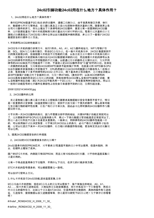
二、24c02芯片硬件介绍:1、引脚说明:A0,A1,A2——地址输入引脚,走位硬件寻址的依据,同种芯片可同时连接8片(2^3);Vcc,Gnd——电源,接地引脚,1.8-5.5vWp——写保护,当Wp接地时,允许对器件的正常读写操作;当Wp接高电平时,写保护,只能进行读操作。
SDA——串行地址/数据输入/输出端口,双向传输,漏极开路,需外接上拉电阻到Vcc(典型阻值为10k)。
SCL——串行时钟输入,高低电平不同状态与SDA配合,执行不同的命令。
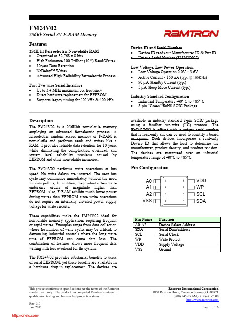
2、存储结构:24c02的容量是2k,256字节。
24C02/24C04/24C08/24C16/24C32/24C641.2.2K4K 8K ,16K ,32K 位和64K 位串行I C 总线EEPROM3.24C02/04/08/16/32/64PROM256/512/1024/2048/4096/8192×8-bit1.8V1μA1mA 24C02/04/08/16/32/648/16/16/16/32/3224C02/04/08/16/32/648-pin PDIP8-pin SOP ●●●●●●●●●●●●SD SCL WP V CC NC A SD A SCL WP V CC 12348765NC NC NC GND SD A SCL WP V CC 12348765 ()SD A SCL WP V CC 12348765A 0A 1A 2GND C02C1621.8V~5.5V- 1mA- 1μA- 24C02, 256 X 8 (2K bits)- 24C04, 512 X 8 (4K bits) - 24C08, 1024 X 8 (8K bits) - 24C16, 2048 X 8 (16K bits)- 24C32, 4096 X 8 (32K bits)- 24C64, 8192 X 8 (64K bits)2I CI C 1 MHz (5V), 400 kHz (1.8V, 2.5V, 2.7V) ( 5 ms)8 (24C02)16(24C04/08/16),32字节页(24C32/64)ESD 2.5kV - 100- 100 8-pin DIP 8-pin SOP RoHS ●●●●●●●22●S D A 123487651A 2GND NC NC C A 2GND C04C082.7V)00n SOP●●SD A SCL WP V CC 12348765A 0A 1A 2GND C32SD ASCL WP V CC 12348765A 0A 1A 2GNDC6424C02/24C04/24C08/24C16/24C32/24C645. Ḛ1 ḚV 6. 乱 ヺ ԡⳈ⌕կ⬉⬉ Ⳉ⌕䕧 ⬉ ⏽V CC Ⳉ⌕䕧 ⬉ V IN V OUT T STG -0.3 ~ V CC +0.3-0.3 ~ V CC +0.3-0.3 ~ +6.5°C -65 ~ +150V °C7. 㤤 ӊヺ ԡⳈ⌕կ⬉⬉ V CC ⏽T A+855.5 1.8-40(䍙 乱 㛑Ӯ 㟈 ӊ )V V ( 㤤 ӊϟ ⦄ 㛑)SDASCL WP V CCNC /NC /NC /A0NC /NC /A1/A1NC /A2/A2/A2C16/C08/C04/C02GNDSTART STOPLOGICSERIAL CONTROLLOGICDEVICE ADDRESS COMPARATORDATA WORD ADDRESS COUNTER LOADCOMPLOADINCY DECODER HIGH VOLTAGE PUMP/TIMING ENDATA RECOVERYEEPROMSERIAL MUXX D E C O D E RDOUT/ACKNOWLEDGEDINESD ⬉ (Ҏԧ )ESD ⬉ ( )V ESD2500200V V乱⬉ 䕧 ⬉ 乱 㛑Ӯ 㟈 ӊ DOUTmA 9. Ⳉ⌕⬉⇨⡍ヺ ԡ ⬉⌕կ⬉⬉⌕I CC V CC =5V⌟䆩 ӊ100kHz 3.0䕧 Ԣ⬉ ⬉μA 3.01.0-0.6V 0.4V IN = V CC GND 0.05( ӊ˖T A = 0°C ̚ +70°C, V CC = +1.8V ̚ +5.5V ˈ䰸䴲 ⊼䞞)䕧 Ԣ⬉ ⬉ μA V IL 0.4V CC0.20.4100kHz V V CC ×0.3I SB V IN = V CC GND V OUT = V CC GND μA 䕧 ⓣ⬉⌕䕧 ⓣ⬉⌕I LI I LO V IH 䕧 催⬉ ⬉ V CC +0.5V V V VV OL3V OL2V = 2.1 mA V 10. Ѹ⌕⬉⇨⡍ ( ӊ˖T A = 0°C ̚ +70°C, V = +1.8V +5.5V, C L = 100 pF ˈ䰸䴲 ⊼䞞)ヺ ԡ䩳催⬉䩳乥⥛, SCL ⌟䆩 ӊ400V CC =1.8V 1000ns 0.050.050.60.90.6 μskHz 1.20.5540V CC =5V 0.4t LOW μs ⍜䰸 䯈 䩳ϟ䰡⊓ 䕧 䯈䱨 䯈t I t AA50t HIGH䩳Ԣ⬉ μsV CC =1.8V V CC =5V V CC =1.8V V CC =5V V CC =1.8V V CC =5V V CC =1.8V V CC =5V8. 㛮⬉( ӊ˖T A = 25°C, f = 1.0 MHz, V CC = +1.8V)pFヺ ԡ䕧 /䕧 ⬉ (SDA)C I/O 䕧 ⬉ (A0, A1, A2, SCL)C IN68 pF⌟䆩 ӊV I/O = 0V V IN = 0V1.2 㒓䞞 䯈t BUF0.5μs V CC =1.8V V CC =5V䇏1.03.0 mA m 042.0C =5.0V, I OL = 3.0 mA CC ×0.7GNDOL1V CC =3.0V, I OL =2.1mA CC =1.8V, I OL = 0.15 mA =C CC = +1.8V ̚+5.5f SCL10. Ѹ⌕⬉⇨⡍ (㓁)䕧 Ϟ 䯈 䕧 䯈0ns500.650.25ns t WRns 100ns ℶ ӊ ゟ 䯈 䕧 䯈t R t DH t F 䕧 ゟ 䯈μs ms䕧 ϟ䰡 䯈t SU.STOV CC =1.8V V CC =5V V CC =1.8V V CC =5Vμs 300100300t HD.DAT t SU.DAT 2 㒓3SCLSDA_INSDA _OUTt F t LOWt SU .STAt HD.STAt AA t DHt BUFt SU.STOt Rt HD.DAT t SU.DAT t HIGH t LOW8th BIT SCLSDAACKSTOPCONDITIONSTART CONDITIONt WR (1)t HD.STAμs 䍋 ӊ 䯈䍋 ӊ ゟ 䯈t SU.STA V CC =1.8V V CC =5V V CC =1.8V V CC =5Vμs 0.60.250.60.25ヺ ԡ ⌟䆩 ӊ ⊼ 䯈W :5 ҢϔϾ ⱘ ℶ ӊ 㟇 䚼 㒧 ⱘ 䯈DŽn 08V μ3001AHIG11.3156247A0A1A2SDA SCL WP GND V CCA2A1A024C02/32/64A2A1A0824C02/32/6424C04A2A1424C04A024C08A2224C08A0A124C1616KA2A1A0/SDA V CC10kΩSCL8WP WPWPV CC12.13. 䆺㒚 䇈24CXX I C 㒓Ӵ䕧 䆂DŽI C ϔ⾡ ǃϸ㒓І㸠䗮䆃 ˈ І㸠 㒓SDA І㸠 䩳㒓SCL DŽϸḍ㒓䛑 乏䗮䖛ϔϾϞ ⬉䰏 ⬉⑤DŽ ⱘ 㒓䜡㕂 4 ⼎4 ϸ㒓 㒓䜡㕂㒓Ϟ 䗕 ⱘ ӊ㹿⿄ 䗕 ˈ ⱘ ӊ㹿⿄ DŽ Ѹ ⱘ ӊ㹿⿄Џ ӊˈ Џ ӊ ⱘ ӊ 㹿⿄Ң ӊDŽЏ ӊѻ⫳І㸠 䩳SCL ˈ㒓ⱘ䆓䯂⢊ ǃѻ⫳START STOP ӊDŽ24CXX I C 㒓ЁЎҢ ӊ DŽ㒓 Ѣぎ䯆⢊ ҹ Ӵ䕧DŽ↣ Ӵ䕧 ѢSTART ӊˈ㒧 ѢSTOP ӊˈѠ㗙П䯈ⱘ 㡖 ≵ 䰤 ⱘˈ⬅ 㒓ϞⱘЏ ӊ DŽ ҹ 㡖˄8ԡ˅Ў ԡӴ䕧ˈ9ԡ ⬅ ѻ⫳ ㄨDŽ䍋 ℶ ӊ䩳㒓䛑Ў催 ⿄ 㒓 ぎ䯆⢊ DŽ SCL Ў催⬉ SDA ⱘϟ䰡⊓˄催 Ԣ 䍋 ӊ˄START ˈㅔ ЎS ˅ˈSDA ⱘϞ ⊓˄Ԣ 催˅ ℶ ӊ˄STOP ˈㅔ ЎP ˅DŽ 㾕 5DŽ5 䍋 ӊ ℶ ӊⱘ НV CCҪ24Cxx MPU SDASCLR PR Pϸ㒓І㸠S Ў催ㅔ ЎⱘϞ ⊓˄Ԣ 㒓І㸠 㒓SS 䍋 ӊ222ԡӴ䕧↣Ͼ 䩳㛝 Ӵ䗕ϔԡ DŽSCL Ў催 SDA 乏 〇 ˈ Ўℸ SDA ⱘ 㹿䅸Ў DŽԡӴ䕧 㾕 6DŽ6 ԡӴ䕧ㄨ㒓Ϟⱘ ↣ ϔϾ 㡖 ѻ⫳ϔϾ ㄨˈЏ ӊ 乏ѻ⫳ϔϾ ⱘ乱 ⱘ 䩳㛝 ˈ㾕 7DŽ7 I C㒓ⱘ ㄨ ԢSDA 㒓㸼⼎ ㄨˈ ㄨ㛝 䯈 〇 ⱘԢ⬉ DŽ Џ ӊ ˈ 乏 Ӵ䕧㒧 ⱘ 㒭 䗕 ˈ ϔϾ 㡖П ⱘ ㄨ㛝 䯈ϡӮѻ⫳ ㄨ ˄ϡ ԢSDA ˅DŽ䖭⾡ ϟˈ 䗕 乏䞞 SDA 㒓Ў催ҹ Џ ӊѻ⫳ ℶ ӊDŽ䗕 䕧 ⱘ䕧 ⱘЏ ӊ ⱘ䍋 ӊ289䴲 ㄨㄨㄨ 䩳㛝㒓〇䆌SDASCL2ѻ⫳ϔϾ ㄨˈЏ ӊ 乏ѻ⫳ϔԢ㒓Ӵӊ ⱘSCL 䍋 ӊS1ӊ䍋 ӊՓ㛑㢃⠛䇏 ˈEEPROM 䛑㽕∖ 8ԡⱘ ӊ ˄㾕 8˅DŽӊ ⬅"1"ǃ"0" 㒘 ˈ 4ԡ Ё ⼎ˈ Ѣ І㸠EEPROM 䛑 ϔḋⱘ Ѣ24C02/32/64ˈ䱣 3ԡA2ǃA1 A0Ў ӊ ԡˈ 乏Ϣ⹀ӊ䕧 㛮 ϔ㟈DŽ Ѣ24C04ˈ䱣 2ԡA2 A1Ў ӊ ԡˈ 1ԡЎ义 ԡDŽA2 A1 乏Ϣ⹀ӊ䕧 㛮 ϔ㟈ˈ㗠A0 ぎ㛮DŽѢ24C08ˈ䱣 1ԡA2Ў ӊ ԡˈ 2ԡЎ义 ԡDŽA2 乏Ϣ⹀ӊ䕧 㛮 ϔ㟈ˈ㗠A1 A0 ぎ㛮DŽѢ24C16ˈ ӊ ԡˈ3ԡ䛑Ў义 ԡˈ㗠A2ǃA1 A0 ぎ㛮DŽ ӊ ⱘLSB Ў䇏/ 䗝 ԡˈ催Ў䇏 ˈԢЎ DŽ㢹↨䕗 ӊ ϔ㟈ˈEEPROM 䕧 ㄨ"0"DŽ ϡϔ㟈ˈ 䖨 ⢊ DŽ8 ӊ 1010A2A1A0R/W MSBLSB1010A2A1P0R/W1010A2P1P0R/W1010P2P1P0R/Wӊ EEPROM Ԣ 㗫 ⱘ⡍⚍ˈ ӊЎ˖˄1˅⬉⑤Ϟ⬉˗˄2˅ ℶ ӊ ӏԩ 䚼 DŽ24C0424C0824C16DŽ ԡ䆂Ёѻ⫳Ё ǃ ⬉ ㋏㒳 ԡ ˈI C 㒓 䗮䖛ҹϟℹ偸 ԡ˖ ˄1˅ѻ⫳9Ͼ 䩳 DŽ˄2˅ SCL Ў催 ˈSDA гЎ催DŽ ˄3˅ѻ⫳ϔϾ䍋 ӊDŽ21. 㡖㽕∖ ӊ ACK ㄨ ˈ 8ԡⱘ DŽ 䖭Ͼ EEPROM ㄨ"0"ˈ✊ ϔϾ8ԡ DŽ 8ԡ ˈEEPROM ㄨ"0"ˈ ⴔ 乏⬅Џ ӊ 䗕 ℶ ӊ 㒜ℶ DŽℸ EEPROM 䖯 䚼 t WR ˈ 䴲 Ёˈ ℸ 䯈 䕧 䛑 Ⳉ ˈEEPROM Ӯ ㄨ˄㾕 9˅DŽ9 㡖SDA 㒓䍋 ӊM S BL S B R /W A C K M S BL S B A C KA C Kӊℶ ӊDŽ24C02/32/6413.2.图10页写24C02器件按8字节/页执行页写,24C04/08/16器件按16字节/页执行页写,24C32/64器件按32字节/页执行页写。
FEATURES•Single supply with 5.0V operation •Low power CMOS technology - 1 mA active current typical-10 µ A standby current typical at 5.0V - 5 µ A standby current typical at 5.0V•Organized as a single block of 128 bytes (128 x 8) or 256 bytes (256 x 8)•2-wire serial interface bus, I 2 C compatible •100 kHz compatibility•Self-timed write cycle (including auto-erase)•Page-write buffer for up to 8 bytes• 2 ms typical write cycle time for page-write •Hardware write protect for entire memory •Can be operated as a serial ROM •ESD protection > 3,000V•1,000,000 ERASE/WRITE cycles guaranteed Data retention > 200 years •8 pin DIP or SOIC package•Available for extended temperature ranges DESCRIPTIONThe Microchip T echnology Inc. 24C01B and 24C02B are 1K bit and 2K bit Electrically Erasable PROMs. The devices are organized as a single block of 128 x 8 bit or 256 x 8 bit memory with a 2-wire serial interface. The 24C01B and 24C02B also have page-write capability for up to 8 bytes of data. The 24C01B and 24C02B are available in the standard 8-pin DIP and an 8-pin surface mount SOIC package.These devices are for extended temperature applications only. It is recommended that all other applications use Microchip’s 24LC01B/02B.-Automotive (E):-40˚C to +125˚C2元器件交易网24C01B/02B1.0ELECTRICAL CHARACTERISTICS1.1Maximum Ratings*V CC ...................................................................................7.0V All inputs and outputs w.r.t. V SS ................-0.6V to V CC +1.0V Storage temperature.....................................-65˚C to +150˚C Ambient temp. with power applied.................-65˚C to +125˚C Soldering temperature of leads (10 seconds).............+300˚C ESD protection on all pins............................................. ≥ 4 kV*Notice: Stresses above those listed under “Maximum ratings”may cause permanent damage to the device. This is a stress rat-ing only and functional operation of the device at those or any other conditions above those indicated in the operational listings of this specification is not implied. Exposure to maximum rating conditions for extended periods may affect device reliability.TABLE 1-1:PIN FUNCTION TABLEName FunctionV SS SDA SCL WP V CC NCGroundSerial Address/Data I/O Serial ClockWrite Protect Input +5.0V Power Supply No Internal ConnectionTABLE 1-1:DC CHARACTERISTICSAll parameters apply across the speci-fied operating ranges unless otherwise noted.VCC = +4.5V to 5.5VAutomotive (E):Tamb = -40 ° C to 125 ° C ParameterSymbol Min.Max.Units ConditionsWP , SCL and SDA pins:High level input voltageV IH .7 V CCV Low level input voltageV IL .3 V CC V Hysteresis of Schmidt trigger inputs V HYS .05 V CC —V (Note)Low level output voltage V OL .40V I OL = 3.0 mA, V CC = 2.5V Input leakage current ILI -1010 µ A V IN = .1V to 5.5V Output leakage currentILO -1010 µ mA V OUT = .1V to 5.5VPin capacitance (all inputs/outputs)C IN , C OUT —10pF V CC = 5.0V (Note 1)Tamb = 25˚C, F CLK = 1 MHz Operating current I CC Write —3mA V CC = 5.5V , SCL = 100 kHzI CC Read —1mA Standby current ICCS—30 µ A V CC = 3.0V , SDA = SCL = VCC 100 µ AV CC = 5.5V , SDA = SCL = VCC Note:This parameter is periodically sampled and not 100% tested.元器件交易网24C01B/02BTABLE 1-2:AC CHARACTERISTICSAll Parameters apply across thespecified operating ranges unless otherwise notedVcc = 4.5V to 5.5V Automotive (E):Tamb = -40˚C to +125˚C,ParameterSymbol Min.Max.Units RemarksClock frequency F CLK —100kHz Clock high time T HIGH 4000—ns Clock low time T LOW 4700—ns SDA and SCL rise time T R —1000ns (Note 1)SDA and SCL fall time T F —300ns (Note 1)ST ART condition hold time T HD : STA 4000—ns After this period the first clock pulse is generatedST ART condition setup time T SU : STA 4700—ns Only relevant for repeated ST ART condition Data input hold time T HD : DAT 0—ns (Note 2)Data input setup time T SU : DAT 250—ns STOP condition setup time T SU : STO 4000—ns Output valid from clock T AA —3500ns (Note 2)Bus free timeT BUF 4700—ns Time the bus must be free before a new transmission can start Output fall time from V IH minimum to V IL maximum T OF —250ns (Note 1), CB ≤ 100 pF Input filter spike suppression (SDA and SCL pins)T SP —50ns (Note 3)Write cycle time T WR —10ms Byte or Page modeEndurance—1M—cycles25 ° C, Vcc = 5.0V , Block Mode (Note 4)Note 1:Not 100% tested. CB = total capacitance of one bus line in pF .2:As a transmitter, the device must provide an internal minimum delay time to bridge the undefined region(minimum 300 ns) of the falling edge of SCL to avoid unintended generation of START or STOP conditions.3:The combined T SP and VHYSspecifications are due to Schmitt trigger inputs which provide improved noisespike suppression. This eliminates the need for a TI specification for standard operation.4:This parameter is not tested but guaranteed by characterization. For endurance estimates in a specificapplication, please consult the T otal Endurance Model which can be obtained on our BBS or website.元器件交易网24C01B/02B2.0FUNCTIONAL DESCRIPTION The 24C01B/02B supports a bi-directional two wire bus and data transmission protocol. A device that sends data onto the bus is defined as transmitter, and a device receiving data as receiver. The bus has to be controlled by a master device which generates the serial clock (SCL), controls the bus access, and gener-ates the ST ART and STOP conditions, while the 24C01B/02B works as slave. Both master and slave can operate as transmitter or receiver but the master device determines which mode is activated.3.0BUS CHARACTERISTICSThe following bus protocol has been defined:•Data transfer may be initiated only when the busis not busy.•During data transfer, the data line must remain stable whenever the clock line is HIGH. Changes in the data line while the clock line is HIGH will be interpreted as a ST ART or STOP condition. Accordingly, the following bus conditions have been defined (Figure 3-1).3.1Bus Not Busy (A)Both data and clock lines remain HIGH.3.2Start Data Transfer (B)A HIGH to LOW transition of the SDA line while the clock (SCL) is HIGH determines a ST ART condition. All commands must be preceded by a ST ART condi-tion.3.3Stop Data Transfer (C)A LOW to HIGH transition of the SDA line while the clock (SCL) is HIGH determines a STOP condition. All operations must be ended with a STOP condition.3.4Data Valid (D)The state of the data line represents valid data when, after a ST ART condition, the data line is stable for the duration of the HIGH period of the clock signal.The data on the line must be changed during the LOW period of the clock signal. There is one clock pulse per bit of data.Each data transfer is initiated with a ST ART condition and terminated with a STOP condition. The number of the data bytes transferred between the ST ART and STOP conditions is determined by the master device and is theoretically unlimited, although only the last six-teen will be stored when doing a write operation. When an overwrite does occur it will replace data in a first in first out fashion.3.5AcknowledgeEach receiving device, when addressed, is obliged to generate an acknowledge after the reception of each byte. The master device must generate an extra clock pulse which is associated with this acknowledge bit. The device that acknowledges has to pull down the SDA line during the acknowledge clock pulse in such a way that the SDA line is stable LOW during the HIGH period of the acknowledge related clock pulse. Of course, setup and hold times must be taken into account. A master must signal an end of data to the slave by not generating an acknowledge bit on the last byte that has been clocked out of the slave. In this case, the slave must leave the data line HIGH to enable the master to generate the STOP condition.元器件交易网24C01B/02B3.6Device AddressAfter generating a ST ART condition, the bus master transmits the slave address consisting of a 4-bit device code (1010) for the 24C01B/02B, followed by three don't care bits.The eighth bit of slave address determines if the master device wants to read or write to the 24C01B/02B (Figure 3-2).The 24C01B/02B monitors the bus for its correspond-ing slave address all the time. It generates an acknowl-edge bit if the slave address was true and it is not in a programming mode.4.0WRITE OPERATION4.1Byte WriteFollowing the start signal from the master, the device code (4 bits), the don't care bits (3 bits), and the R/W bit which is a logic low is placed onto the bus by the master transmitter. This indicates to the addressed slave receiver that a byte with a word address will follow after it has generated an acknowledge bit during the ninth clock cycle. Therefore the next byte transmitted by the master is the word address and will be written into the address pointer of the 24C01B/02B. After receiving another acknowledge signal from the 24C01B/02B the master device will transmit the data word to be written into the addressed memory location.The 24C01B/02B acknowledges again and the master generates a stop condition. This initiates the internal write cycle, and during this time the 24C01B/02B will not generate acknowledge signals (Figure 4-1).4.2Page WriteThe write control byte, word address and the first data byte are transmitted to the 24C01B/02B in the same way as in a byte write. But instead of generating a stop condition the master transmits up to eight data bytes to the 24C01B/02B which are temporarily stored in the on-chip page buffer and will be written into the memoryafter the master has transmitted a stop condition. After the receipt of each word, the three lower order address pointer bits are internally incremented by one. The higher order five bits of the word address remains con-stant. If the master should transmit more than eight words prior to generating the stop condition, the address counter will roll over and the previously received data will be overwritten. As with the byte write operation, once the stop condition is received an inter-nal write cycle will begin (Figure 4-2).元器件交易网24C01B/02B5.0ACKNOWLEDGE POLLINGSince the device will not acknowledge during a write cycle, this can be used to determine when the cycle is complete (this feature can be used to maximize bus throughput). Once the stop condition for a write com-mand has been issued from the master, the device ini-tiates the internally timed write cycle. ACK polling can be initiated immediately. This involves the master send-ing a start condition followed by the control byte for a write command (R/W = 0). If the device is still busy with the write cycle, then no ACK will be returned. If the cycle is complete, then the device will return the ACK and the master can then proceed with the next read or write command. See Figure 5-1 for flow diagram. FIGURE 5-1:ACKNOWLEDGE POLLING6.0WRITE PROTECTIONThe 24C01B/02B can be used as a serial ROM when the WP pin is connected to V CC. Programming will be inhibited and the entire memory will be write-protected.7.0READ OPERATIONRead operations are initiated in the same way as write operations with the exception that the R/W bit of the slave address is set to one. There are three basic types of read operations: current address read, random read, and sequential read.7.1Current Address ReadThe 24C01B/02B contains an address counter that maintains the address of the last word accessed, inter-nally incremented by one. Therefore, if the previous access (either a read or write operation) was to address n, the next current address read operation would access data from address n + 1. Upon receipt of the slave address with R/W bit set to one, the 24C01B/ 02B issues an acknowledge and transmits the eight bit data word. The master will not acknowledge the trans-fer but does generate a stop condition and the 24C01B/ 02B discontinues transmission (Figure 7-1).7.2Random ReadRandom read operations allow the master to access any memory location in a random manner. T o perform this type of read operation, first the word address must be set. This is done by sending the word address to the 24C01B/02B as part of a write operation. After the word address is sent, the master generates a start condition following the acknowledge. This terminates the write operation, but not before the internal address pointer is set. Then the master issues the control byte again but with the R/W bit set to a one. The 24C01B/02B will then issue an acknowledge and transmits the eight bit data word. The master will not acknowledge the transfer but does generate a stop condition and the 24C01B/02B discontinues transmission (Figure 7-2).7.3Sequential ReadSequential reads are initiated in the same way as a ran-dom read except that after the 24C01B/02B transmits the first data byte, the master issues an acknowledge as opposed to a stop condition in a random read. This directs the 24C01B/02B to transmit the next sequen-tially addressed 8-bit word (Figure 7-3).To provide sequential reads the 24C01B/02B contains an internal address pointer which is incremented by one at the completion of each operation. This address pointer allows the entire memory contents to be serially read during one operation.7.4Noise ProtectionThe 24C01B/02B employs a V CC threshold detector cir-cuit which disables the internal erase/write logic if the V CC is below 1.5 volts at nominal conditions.The SCL and SDA inputs have Schmitt trigger and filter circuits which suppress noise spikes to assure proper device operation even on a noisy bus.元器件交易网24C01B/02B8.0PIN DESCRIPTIONS8.1Serial DataThis is a bi-directional pin used to transfer addresses and data into and data out of the device. It is an open drain terminal, therefore the SDA bus requires a pull-up resistor to V CC (typically 10 KΩ for 100 kHz).For normal data transfer SDA is allowed to change only during SCL low. Changes during SCL high are reserved for indicating the ST ART and STOP condi-tions.8.2SCL Serial ClockThis input is used to synchronize the data transfer from and to the device.8.3WPThis pin must be connected to either V SS or V CC.If tied to V SS, normal memory operation is enabled (read/write the entire memory).If tied to V CC, WRITE operations are inhibited. The entire memory will be write-protected. Read operations are not affected.This feature allows the user to use the 24C01B/02B as a serial ROM when WP is enabled (tied to V CC).元器件交易网元器件交易网24C01B/02B Array NOTES:元器件交易网24C01B/02B Array NOTES:元器件交易网24C01B/02B Array NOTES:24C01B/02BT o order or obtain information, e.g., on pricing or delivery, refer to the factory or the listed sales office.Data SheetsProducts supported by a preliminary Data Sheet may have an errata sheet describing minor operational differences and recom-mended workarounds. To determine if an errata sheet exists for a particular device, please contact one of the following:1.Y our local Microchip sales office.2.The Microchip Corporate Literature Center U.S. FAX: (602) 786-7277.3.The Microchip’s Bulletin Board, via your local CompuServe number (CompuServe membership NOT required).Please specify which device, revision of silicon and Data Sheet (include Literature #) you are using.元器件交易网元器件交易网MAll rights reserved. © 1997, Microchip T echnology Incorporated, USA. 12/97 Printed on recycled paper.。