霍尔传感器中文手册
- 格式:doc
- 大小:556.65 KB
- 文档页数:7
~ 1 ~ © 2014 深圳响拇指电子科技有限公司
全极霍尔效应传感器IC SS239资料及应用
概述:
SS239是一款采用混合信號CMOS 技術的全極霍爾效應傳感IC 器件。
它集成了先進的斬波穩定技術,這使得該器件能提供准確而穩定的磁開關工作點。
優點和特性
- 工作電壓可低至2。
5V
- CMOS 技術
- 非常適用於電池供電應用的微功耗技術
- 高靈敏度,能直接替代磁簧開關
- 對應南北極磁場強度絕對值的全極輸出開關
- 優化的睡眠模式極大的延長了其使用壽命
- 均符合RoHS 標准的小尺寸SOT233L 或SIP3L 封裝
應用實例:固態開關、手持式無線話筒喚醒開關、電池供電設備的蓋關閉傳感器、磁近感傳感器可用於低占空比應用中簧片開關的替代
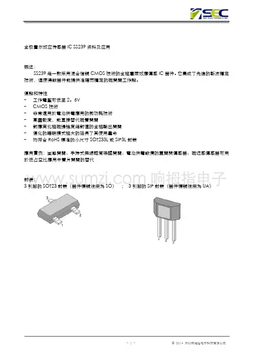
封装:
3引腳的SOT23封裝(器件標號後綴為SO ) ; 3引腳的SIP 封裝(器件標號後綴為UA )。
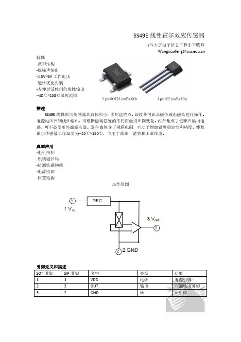
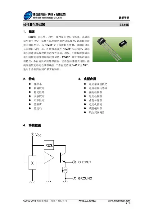
SS49E线性霍尔效应传感器山西大学电子信息工程系王晓峰Wangxiaofeng@ 特性-微型结构-低噪声输出-4.5V~6V工作电压-磁性优化封装-方便灵活使用的线性输出--40℃~150℃温度范围描述SS49E线性霍尔传感器具有体积小,多用途特点。
该设备可由永磁体或电磁铁进行操作。
电源电压控制线性输出,可根据磁场强度的不同而做成比例变化。
内部集成了低噪声输出电路,可不必使用外部滤波器。
器件也包含了薄膜电阻,有助于增加温度稳定性和精度。
线性霍尔传感器工作温度为--40℃~150℃,可用于商业,消费和工业环境。
典型应用-电机控制-识读磁性码-侦测铁磁物质-电流检测-位置检测功能框图引脚定义和描述SOT引脚SIP引脚名字类型功能11VDD电源电源引脚23OUT输出开漏输出引脚32GND地地引脚最大极限参数参数符号值单位电源电压(工作状态)VCC8.0V输出电流Iout20mA工作温度范围TA-40~150℃储存温度TS-65~150℃电气参数(TA=25℃,VCC=5.0V)参数符号测试条件最小典型最大单位工作电压VCC正常工作 3.0 6.5V电源电流ICC平均 4.28.0mA 输出电流IOUT 1.0 1.5mA 反应时间Tack3uS静态输出电压VO B=0G 2.25 2.5 2.75V灵敏度ΔVOUT TA=25℃ 2.0 2.5 3.0mV/G 最小输出电压B=-1500G0.86V最大输出电压B=1500G 4.21V线性度-0.007-0.100.10%/℃温度误差(零漂)灵敏度漂移TA≥25℃-0.150.05%/℃TA<25℃-0.040.185%/℃后缀UA,3脚单列直插后缀SO,3脚SOT-23封装订购信息文档版本信息2013年11月1日,V3.10版。
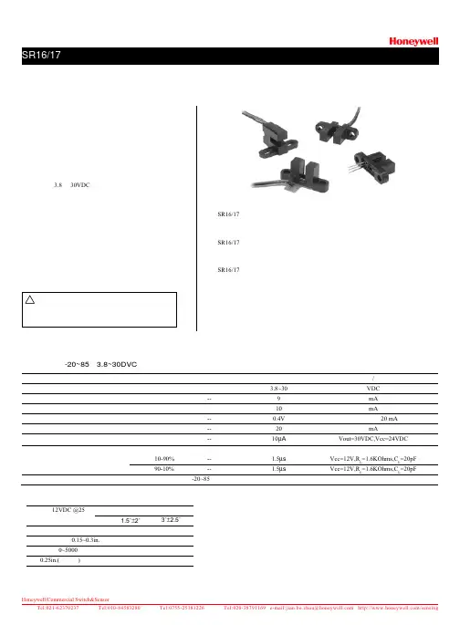
操作范围12VDC @25℃条件目标物感应距离 0.15~0.3in.每分钟转数 0~5000槽深 0.25in.(最小值)特点:●结构紧凑、密封坚固● 机械上可与其他标准光电传感器互换 ● 含铁金属叶片插入的工作原理 ● 用于脉冲计数和位置感应 ● 电流沉(集电极开路)输出 ● 供电电源3.8—30VDC● 使用中等强度磁铁以减少对周边区域的影响 ● 内部密封适用于普通环境的应用 ● 无机械触点,免除磨损 ● 非接触性位置感应SR16/17系列霍尔效应槽式传感器,用于位置检测和速度检测感应,提供侧面封装和三种端子类型。
SR16/17系列传感器具有较高的性价比,适用于中度的电气、化学和机械环境。
SR16/17系列传感器包括内置的磁铁和霍尔效应传感器,被封装在槽形外壳中。
典型应用:用户的铁磁目标物体通过槽间时,磁场被干扰,转换成传感器的开关量输出。
霍尔传感器被密封在塑料外壳中。
在灰尘的环境中可以保证高精度和重复性,而光电传感器无法达到。
其封装材料使用聚碳酸酯,机械上可与霍尼韦尔的标准槽式光电传感器互换。
电气特性(-20~85,3.8~30DVC )供电电源消耗电流(释放)消耗电流(工作)输出电压(工作)电流沉(工作)输出漏电流(释放)输出开关时间上升,10-90%下降,90-10%工作温度-20~85℃(最小值)------------(最大值)3.8~309100.4V 2010µA1.5µs 1.5µs单位/条件VDC mA mA最大沉电流20 mAmAVout=30VDC,Vcc=24VDCVcc=12V,R L =1.6KOhms,C L =20pF Vcc=12V,R L =1.6KOhms,C L =20pF机械特性操作1.5˚±2˚释放3˚±2.5˚!警告不要把此产品用于安全式紧急止动场合。
(产品的失效将导制人身安全的损坏。
)内部电路框图速度检测接口封装尺寸mm/inSR16C-J6SR16C-NSR16C-J4SR17C-J6霍尔传感器触发器和放大器Notes:1. Mounting specification: non-ferrous #4 machine head screws with .25 OD washers torqued to 3-5 in-lbs.2. Suggested target configuration, material: .045 low carbon steel, high permeability, low residual induction.3. Operate (degrees) is the angular distance from the leading edge of the tooth to the centerline of the sensor.4. Release (degrees) is the angular distance from the trailing edge of the tooth to the centerline of the sensor.5. Operating specification is based on target shown.供电电压输出(常态高电平)接地接地,黑色 供电,红色 输出,绿色。
1
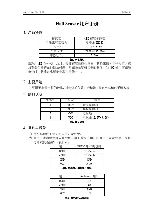
Hall Sensor 用户手册
1. 产品特性
原理:49E 为小型、通用、线性霍尔效应传感器,其输出信号电平决定于施加在器件敏感面的磁场强度,随磁场强度成比例的变化,当49E 处于零磁场条件时,其输出电压是电源电压的一半。
2. 主要用途
主要用于测量电机的转速,对物体的位置进行检测,智能小车和电子积木等。
3. 接口说明
4. 操作与现象
① ②
③把传感器靠近磁铁时,模块上的信号指示灯点亮.
传感器远离磁铁时,模块上的信号指示灯熄灭。
随着传感器与金属接触与分离,串口输出的数据会发生相应改变。
2。
1.霍尔传感器霍尔电流传感器主要适用于交流、直流、脉冲等复杂信号的隔离转换,通过霍尔效应原理使变换后的信号能够直接被AD 、DSP 、PLC 、二次仪表等各种采集装置直接采集,广泛应用于电流监控及电池应用、逆变电源及太阳能电源管理系统、直流屏及直流马达驱动、电镀、焊接应用、变频器,UPS 伺服控制等系统电流信号采集和反馈控制,具有响应时间快,电流测量范围宽精度高,过载能力强,线性好,抗干扰能力强等优点。
1.1开环霍尔电流传感器1.1.1型号说明1.1.2技术指标技术参数指标霍尔开口式/闭口式开环霍尔(真有效值)输出标称值电压:±5V/±4V 电流:4~20mA 零点失调电压(电流)电压:±20mV电流:±0.05mA失调电压(电流)漂移电压:≤±1.0mV/℃电流:±0.04mA/℃线性度≤0.2%FS电源电压DC ±15V DC 24V频宽0~20kHz 响应时间≤5us≤1ms耐压强度输入与输出及电源之间允许AC2500V 工频耐压精度等级1.0环境温度工作:-25℃~+70℃;储存:-40℃~+85℃湿度≤95%RH,不结露,无腐蚀性气体场所海拔≤3500m注:开口式、闭口式为传感器产品外观不同,原理都为开环原理。
1.1.3开口式开环霍尔电流传感器1.1.3.1规格尺寸(单位:mm)图1图21.1.3.2规格参数对照表型号额定电流供电电源额定输出测量孔径(mm)准确度AHKC-EKA 0~(50-500)A ±15V 5V /4V φ201级AHKC-EKAADC 0~(50-500)A12V/24V4~20mAφ201级尺寸规格外形尺寸穿孔尺寸安装尺寸图形W H D a e ΦM N AHKC-EKA 606416//2047/图1AHKC-EKAA 606416//2047/图1AHKC-EKDA 606416//2047/图1AHKC-EKB 10010224//4080/图1AHKC-EKBA 10010224//4080/图1AHKC-EKBDA 10010224//4080/图1AHKC-EKC 11511027//6095.5/图1AHKC-EKCA 11511027//6095.5/图1AHKC-EKCDA 11511027//6095.5/图1AHKC-K 12763256416//30图2AHKC-KAA 12763256416//30图2AHKC-KDA 12763256416//30图2AHKC-H 14979258232//46图2AHKC-KA 17695.52910436//60图2AHKC-HB 204111.52913252//48×2图2AHKC-HBAA 204111.52913252//48×2图2AHKC-HBDA204111.52913252//48×2图2AHKC-EKDA AC 0~(50-500)A 12V/24V 4~20mA φ201级AHKC-EKB 0~(200-1000)A±15V 5V /4V φ401级AHKC-EKBADC 0~(200-1000)A 12V/24V4~20mAφ401级AHKC-EKBDA AC 0~(200~1000)A 12V/24V 4~20mA φ401级AHKC-EKC 0~(500-1500)A±15V 5V /4V φ551级AHKC-EKCADC 0~(500-1500)A 12V/24V4~20mAφ551级AHKC-EKCDA AC 0~(500-1500)A 12V/24V 4~20mA φ551级AHKC-K 0~(400-2000)A±15V 5V /4V 64×161级AHKC-KAA DC 0~(400-2000)A 12V/24V4~20mA64×161级AHKC-KDAAC 0~(400-2000)A12V/24V 4~20mA 64×161级AHKC-H 0~(500-3000)A ±15V 5V /4V 82×321级AHKC-KA 0~(500-5000)A±15V 5V /4V 104×361级AHKC-HB0~(2000-20000)A±15V5V /4V132×521级AHKC-HBAA DC 0~(2000-20000)A12V/24V 4~20mA 132×521级AHKC-HBDA AC 0~(2000-20000)A12V/24V 4~20mA 132×521级注:额定电流未标注表示输入电流交直流均可测量,订货时请注明。

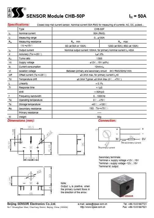
Specifications: Closed loop Hall current sensor, Nominal current 50A RMS for measuring of currents: AC, DC, pulsed …TypeCHB-50P I N Nominal current 50A (RMS) I P Measuring range 0 (100)R M Measuring resistance R M min R M max(Vc =±15V ) 0Ω (at 50A or 100A)120Ω (at 50A); 85Ω (at 100A)I M Output current Nominal output current 100mA, for primary nominal current I N =50AX Accuracy (Ta =+25)℃ I N ±1.0% K N Turns ratio 1:500 Vc Supply voltage ±12V …15V (±5%)Ic Current consumption 10mA+I MVi Isolation voltageBetween primary and secondary circuit: 3KV RMS/50Hz/1min.Ioff Offset current (Ta =+25℃) ±0.3mA max, for primary current I N =0 Td Temperature drift ±0.3mA Typical; ±0.5mA Max (0℃…+70)℃L Linearity < 0.1% Tr Response time < 1μS di/dt> 50A/μS f Frequency bandwidth 0…100KHz Ta Operating temperature 0℃…+70℃ Ts Storage temperature -40℃…+100℃ Rs Secondary resistance 15Ω(Ta =+70℃)Primary resistance ----- WWeight50gDimensions (mm): Connection:+M-0VI N primary currentI M secondary current-+Secondary terminals:Terminal +: supply voltage +12V …15V Terminal -: supply voltage -12V …15V Terminal M: outputNote:Output I M is positive, when the primary current flows in the direction of the arrow.Specifications: Closed loop Hall current sensor, Nominal current 100A RMS for measuring of currents: AC, DC, pulsed …TypeCHB-100P I N Nominal current 100A (RMS) I P Measuring range 0 (150)R M Measuring resistance R M min R M max(Vc =±15V ) 0Ω (at 50A or 100A)130Ω (at 50A); 85Ω (at 100A)I M Output current Nominal output current 100mA, for primary nominal current I N =100AX Accuracy (Ta =+25)℃ I N ±0.8% K N Turns ratio 1:1000 Vc Supply voltage ±12V …15V (±5%)Ic Current consumption 10mA+I MVi Isolation voltageBetween primary and secondary circuit: 3KV RMS/50Hz/1min.Ioff Offset current (Ta =+25℃) ±0.3mA max, for primary current I N =0 Td Temperature drift ±0.3mA Typical; ±0.5mA Max (0℃…+70)℃L Linearity < 0.1% Tr Response time < 1μS di/dt> 50A/μS f Frequency bandwidth 0…100KHz Ta Operating temperature 0℃…+70℃ Ts Storage temperature -40℃…+100℃ Rs Secondary resistance 15Ω(Ta =+70℃)Primary resistance ----- WWeight50gDimensions (mm): Connection:+M-0VI N primary currentI M secondary current-+Secondary terminals:Terminal +: supply voltage +12V …15V Terminal -: supply voltage -12V …15V Terminal M: outputNote:Output I M is positive, when the primary current flows in the direction of the arrow.。
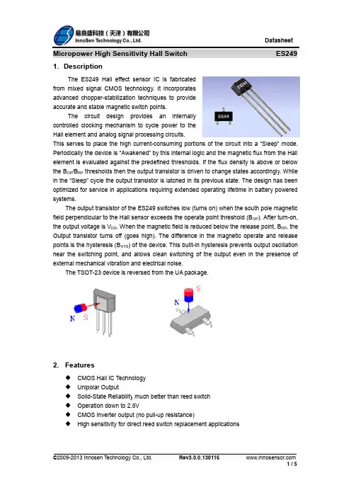
车用霍尔传感器MLX92211数据手册PDFFeatures and BenefitsWide operating voltage range : from 2.7V to 24VVery high magnetic sensitivity : +/-3mT typicalChopper-stabilized amplifier stageBuilt-in negative temperature coefficient : -1100ppm/degC ?Reverse Supply Voltage ProtectionOutput Current Limit with Auto-ShutoffUnder-Voltage Lockout ProtectionThermal ProtectionHigh ESD rating / Excellent EMC performanceThin SOT23 3L Green Compliant package Application ExamplesAutomotive, Consumer and Industrial ?Solid-state switch3-phase BLDC motor commutation ?Wiper motorWindow lifterSunroof/Tailgate openerSeat motor adjusterElectrical power steering1Functional Diagram2General DescriptionThe Melexis MLX92211 is the second generation Hall-effect latch designed in mixed signal CMOS technology. The device integrates a voltage regulator, Hall sensor with advanced offset cancellation system and an open-drain output driver, all in a single package.Based on a brand new platform, the magnetic core is using an improved offset cancellation system allowing faster and more accurate processing while being temperature insensitive and stress independent. In addition is implemented a negative temperature coefficient of -1100ppm/degC to compensate the natural behaviour of magnets becoming weaker with rise in temperature. The included voltage regulator operates from 2.7 to 24V, hence covering a wide range of applications. With the built-in reverse voltage protection, a serial resistor or diode on the supply line is not required so that even remote sensors can be specified for low voltage operation down to 2.7V while being reverse voltage tolerant.In the event of a drop below the minimum supply voltageduring operation, the under-voltage lock-out protection will automatically freeze the device, preventing the electrical perturbation to affect the magnetic measurement circuitry. The output state is therefore only updated based on a proper and accurate magnetic measurement result.The open drain output is fully protected against short-circuit with a built-in current limit. An additional automatic output shut-off is activated in case of a prolonged short-circuit condition. A self-check is then periodically performed to switch back to normal operation if the short-circuit condition is released.The on-chip thermal protection also switches off the output if the junction temperature increases above an abnormally high threshold. It will automatically recover once the temperature decreases below a safe value. With latching magnetic characteristics, the output is turned low or high respectively with a sufficiently strong South or North pole facing the package top side. When removing the magnetic field, the device keeps its previous state.The MLX92211 is delivered in a Green compliant 3-pin Thin Small Outline Transistor (TSOT) for surface-mount process.Table of Contents1 Functional Diagram (1)2 General Description (1)3 Glossary of Terms (3)4 Absolute Maximum Ratings (3)5 General Electrical Specifications (4)6 Magnetic Specifications (5)7 Output Behaviour versus Magnetic Pole (5)8 Performance Graphs (6)8.1 Magnetic parameters vs. T A (6)8.2 Magnetic parameters vs. V DD (6)8.3 V DSon vs. T A (6)8.4 V DSon vs. V DD (6)8.5 I DD vs. T A (6)8.6 I DD vs. V DD (6)8.7 I LEAK vs. T A (7)8.8 I LEAK vs. V DD (7)8.9 Power Derating vs. T A (7)9 Application Information (8)9.1 Typical Three-Wire Application Circuit (8)9.2 Automotive and Harsh, Noisy Environments Three-Wire Circuit (8)10 Standard information regarding manufacturability of Melexis products with different soldering processes (9)11 ESD Precautions (9)12 Package Information (10)12.1 SE Package (TSOT-3L) (10)12.2 Pin Definitions and Descriptions (10)13 Disclaimer (11)3Glossary of TermsMilliTesla (mT), Gauss Units of magnetic flux density: 1mT = 10 GaussRoHS Restriction of Hazardous SubstancesTSOT Thin Small Outline Transistor (TSOT package) –also referred with the Melexis packagecode “SE”ESD Electro-Static Discharge4Absolute Maximum Ratingsfor extended periods may affect device reliability.1 The maximum junction temperature should not beexceeded2 For maximum 1 hour3 Including current through protection device4 For maximum 1s5 Through protection device6 For VOUT ≤27V.7 For 1000 hours.8 Human Model according AEC-Q100-002 standard9 Machine Model according AEC-Q100-003 standard10 Charged Device Model according AEC-Q100-011 standard mA C C C5 General Electrical Specifications1 Typical values are defined at T A = +25oC and V DD = 12V, unless otherwise specified 2Guaranteed by design and verified by characterization, not production tested 3R PU and V PU are respectively the external pull-up resistor and pull-up power supply 4If the Output is in Current Limitation longer than t CLON the Output is switched off in high-impedance state. The Output returns back in active state at next reaching of B OP or after t CLOFF time interval 5The Delay Time is the time from magnetic threshold reached to the start of the output switching 6Output jitter is the unpredictable deviation of the Delay time 7Maximum switching frequency corresponds to the maximum frequency of the applied magnetic field which is detected without loss of pulses 8The Power-On Time represents the time from reaching V DD = V POR to the first refresh of the output (first valid output state) 9Power-On Slew Rate should not be critical for the proper device start-up6 Magnetic Specifications7 Output Behaviour versus Magnetic Poleoo1Temperature Coefficient is calculated using the following formula: C T C T C ppm T T BB B o o o CT T o 150;40;/,10*216122512, value guaranteed by design and verified by characterization, not production tested2 Default Output state during power-up3Magnetic pole facing the branded/top side of the package8Performance Graphs8.1Magnetic parameters vs. T A8.2Magnetic parameters vs. V DD8.3V DSon vs. T A8.4V DSon vs. V DD8.5I DD vs. T A8.6I DD vs. V DD8.7I LEAK vs. T A8.8I LEAK vs. V DD8.9Power Derating vs. T A9Application Information9.1Typical Three-Wire Application CircuitVOUT Notes:1. For proper operation, a 10nF to 100nF bypass capacitor should be placed as close as possible to the V DD and ground pin.2. The pull-up resistor R PU value should be chosen in to limit the current through the output pin below the maximum allowed continuous current for the device.3. A capacitor connected to the output is not needed, because the output slope is generated internally.9.2Automotive and Harsh, Noisy Environments Three-WireCircuitV OUTNotes:1. For proper operation, a 10nF to 100nF bypass capacitor should be placed as close as possible to the V DD and ground pin.2. The device could tolerate negative voltage down to -27V, so if negative transients over supply line V PEAK< -32V are expected, usage of the diode D1 is recommended. Otherwise only R1 is sufficient.When selecting the resistor R1, three points are important: - the resistor has to limit I DD/I DDREV to 50mA maximum - the resistor has to withstand the power dissipated in both over voltage conditions (V R12/R1)- the resulting device supply voltage V DD has to be higher than V DD min (V DD = V CC– R1.I DD)3. The device could tolerate positive supply voltage up to +27V (until the maximum power dissipation is not exceeded), so if positive transients over supply line with V PEAK> 32V are expected, usage a zener diode Z1 is recommended. The R1-Z1 network should be sized to limit the voltage over the device below the maximum allowed.10Standard information regarding manufacturability of Melexis products with different soldering processesOur products are classified and qualified regarding soldering technology, solderability and moisture sensitivity level according to following test methods:Reflow Soldering SMD’s (Surface Mount Devices)IPC/JEDEC J-STD-020Moisture/Reflow Sensitivity Classification for Nonhermetic Solid State Surface Mount Devices(classification reflow profiles according to table 5-2)EIA/JEDEC JESD22-A113Preconditioning of Nonhermetic Surface Mount Devices Prior to Reliability Testing(reflow profiles according to table 2)Wave Soldering SMD’s (Surface Mount Devices) and THD’s (Through Hole Devices)EN60749-20Resistance of plastic- encapsulated SMD’s to combined effect of moisture and solderin g heatEIA/JEDEC JESD22-B106 and EN60749-15Resistance to soldering temperature for through-hole mounted devicesIron Soldering THD’s (Through Hole Devices)EN60749-15Resistance to soldering temperature for through-hole mounted devicesSolderability S MD’s (Surface Mount Devices) and THD’s (Through Hole Devices)EIA/JEDEC JESD22-B102 and EN60749-21SolderabilityFor all soldering technologies deviating from above mentioned standard conditions (regarding peak temperature, temperature gradient, temperature profile etc) additional classification and qualification tests have to be agreed upon with Melexis.The appli cation of Wave Soldering for SMD’s is allowed only after consulting Melexis regarding assurance of adhesive strength between device and board.Melexis is contributing to global environmental conservation by promoting lead free solutions. For more information on qualifications of RoHS compliant products (RoHS = European directive on the Restriction Of the use of certain Hazardous Substances) please visit the quality page on our website: /quality.asp11ESD PrecautionsElectronic semiconductor products are sensitive to Electro Static Discharge (ESD).Always observe Electro Static Discharge control procedures whenever handling semiconductor products.12 Package Information12.1 SE Package (TSOT-3L)SECTION B-B’Notes:1. All dimensions are in millimeters2. Outermost plastic extreme width does not include mold flash or protrusions. Mold flash and protrusions shall not exceed 0.15mm per side.3. Outermost plastic extreme length does not include mold flash or protrusions. Mold flash and protrusions shall not exceed 0.25mm per side.4. The lead width dimension does not include dambar protrusion.Allowable dambar protrusion shall be 0.07mm total in excess of the lead width dimension at maximum material condition.5. Dimension is the length of terminal for soldering to a substrate.6. Dimension on SECTION B-B’ applies to the flat section of the lead between 0.08mm and 0.15mm from the lead tip.7. Formed lead shall be planar with respect to one another with 0.076mm at seating plane.Marking:Tope side : 11YY11 - Part Number (MLX92211)YY – Year (last 2 digits)Bottom side : XXXXXXXX – Lot number (last 4 digits)see note 6TOP VIEWEND VIEWSIDE VIEWNotes:1. All dimensions are in millimeters2. Hall sensor located at package center in X and Y axisTOP VIEW END VIEW13 DisclaimerDevices sold by Melexis are covered by the warranty and patent indemnification provisions appearing in its Term of Sale.Melexis makes no warranty, express, statutory, implied, or by description regarding the information set forth herein or regarding the freedom of the described devices from patent infringement. Melexis reserves the right to change specifications and prices at any time and without notice. Therefore, prior to designing this product into a system, it is necessary to check with Melexis for current information. This product is intended for use in normal commercial applications. Applications requiring extended temperature range, unusual environmental requirements, or high reliability applications, such as military, medical life-support or life-sustaining equipment are specifically not recommended without additional processing by Melexis for each application.The information furnished by Melexis is believed to be correct and accurate. However, Melexis shall not be liable to recipient or any third party for any damages, including but not limited to personal injury, property damage, loss of profits, loss of use, interrupt of business or indirect, special incidental or consequential damages, of any kind, in connection with or arising out of the furnishing, performance or use of the technical data herein. No obligation or liability to recipient or any third party shall arise or flow out of Melexis’ rendering of technical or other services.2005 Melexis NV. All rights reserved.For the latest version of this document, go to our website at Or for additional information contact Melexis Direct:Europe, Africa, Asia:Phone: +32 1367 0495E-mail:************************America:Phone: +1 603 223 2362E-mail:*********************ISO/TS 16949 and ISO14001 Certified。
.霍尔电流传感器
霍尔电流传感器主要适用于交流、直流、脉冲等复杂信号的隔离转换,通过霍尔效应原理使变换后的信号能够直接被AD,DSP、PLC、二次仪表等各种采集装置直接采集和接受,广泛应用于电流监控及电池应用、逆变电源及太阳能电源管理系统、直流屏及直流马达驱动、电镀、焊接应用、变频器,UPS伺服控制等系统电流信号采集和反馈控制,响应时间快,电流测量范围宽精度高,过载能力强,线性好,抗干扰能力强等优点。
2.1开环霍尔电流传感器
2.1.2闭口是开环霍尔电流传感器 固定安装
PCB安装
2.2闭环霍尔电流传感器 固定安装
PCB安装
2.3直流漏电流传感器
2.4D-20开关电源
产品特点:
●低价格、高可靠
●105℃输出电容器
●全球适用AC输入电源
●效率高、工作温度低
●软启动电流、有效降低AC输入冲击●有短路保护、过载保护
●体积小、重量轻
●100%满负荷烧机调试
●内装EMI滤波器、纹波极小。
霍尔传感器主要产品有:该系列产品分为:霍尔开环电流传感器、霍尔闭环电流传感器、霍尔闭环电压传感器、磁调制式直流漏电流传感器、隔离放大器、开关型传感器。
广泛应用于机械、纺织、印刷、汽车、计算机、邮电通讯、电力、自动控制等行业和领域。
霍尔开环电流传感器:简介:霍尔开环系列电流传感器的初、次级之间是绝缘的,可用于测量直流、交流和脉冲电流.电参数:额定输入电流351020305010020030040050060080010001200180020002400测量电流范围915255075150300600900900900900160020002400270030003600300050008000A4500750012000A额定输出电压4±1%V电源电压±15±5%V失调电压25mV失调电压漂移≤±1.0≤±0.5mV/℃线性度≤1%FS响应时间≤7μS绝缘电压50HZ,1min 2.5KV工作温度-40~+85℃储存温度-55~+125℃使用说明:1.当待测电流从传感器穿过,即可在输出端测得电压大小。
(注意:错误的接线可能导致传感器损坏)2.传感器的输出幅度可根据用户需要进行适当调节。
3.可按用户需求定制不同额定输入电流和输出电压的传感器。
霍尔闭环电流传感器:简介:霍尔闭环系列电流传感器的初、次级之间是绝缘的,可用于测量直流、交流和脉冲电流.电参数:额定输入电流0.5 1.0 2.0 5.01020251002003004005001000A 测量电流范围 1.5 3.0 6.0153060501503005006008002000A测量电阻with±15V@±300Amax72(max)@±500Amax40(max)Ω@±500Amax30(max)@±800Amax5(max)Ωwith±18V@±300Amax92(max)@±500Amax60(max)Ω@±500Amax40(max)@±800Amax15(max)Ω匝比1:30001:5000额定输出电流100mA电源电压±15~±18V零电流失调±0.2mA电流失调温漂-40℃~85℃±0.5mA响应时间<1µs线性度≤0.1%FS绝缘电压50HZ,1min6KVdi/dt跟随精度>100A/μs带宽(-3dB)DC…100KHz副边线圈电阻3160Ω工作温度-40~+85℃储存温度-55~+125℃使用说明:1.在IP按箭头方向流动时,IS是正向;2.初级导体温度不应超过100℃;3.母排完全充满初级穿孔时动态表现(di/dt和响应时间)为最佳;4.为了达到最佳的磁耦合,初级线匝应绕在传感器顶部。
1.描述
ES582是单极霍尔效应传感器从混合信号IC制造
CMOS技术。
设备集成了一个电压调节器,霍尔传感器动态
补偿取消系统,施密特触发器和一个open-drain输出驱动程
序,所有在一个包中。
它集成了先进的直升机稳定
技术提供准确和稳定的磁开关点。
有很多申请这HED -霍尔电子设备除了那些下面列出。
由于其宽工作电压范围和扩展温度范围的选择,它非常适用于汽车,工业和消费者应用程序。
交付的设备是在一个小提纲晶体管(说)表面安装过程和在一个塑料单(- 92平)通孔。
3-lead 包都是通过无铅认证。
2.特性
宽工作电压范围3.5 v和24 v
介质的敏感性
CMOS技术
Chopper-stabilized放大级
优良的温度稳定性
极低的开关点漂移
对身体压力
低电流消耗
明渠输出
小SOT23 3 l和平板- 92 3 l,通过无铅认证包
3.应用程序
汽车、消费品和工业
固态开关
断续器
速度检测
线性位置检测
角位置检测
接近detectio
4.原理框图
5.术语表
术语
描述
毫伏特斯拉(mT) 高斯,磁通密度单位:1吨= 10高斯 RoHS
有害物质限制
SOT 小轮廓晶体管(说包)——也被称为包代码” ESD 静电放电 BLDC
Brush-Less 直流
操作点(BOP)
磁通密度应用于品牌的包将输出驱动程序(输出电压= VDSon)
释放点(BRP)
磁通密度应用于品牌的包挫伤了驱动程序的输出(输出电压=高)
6.销的定义和描述
SE 销
UA 销.
类型
函数
名称 1 1 V DD 输入 电源电压销 2 3 OUT 输出 输出销 3
2
GND
接地
地面销
VDD
OUT
V oltage Regulat o r
Chopper
Hall Plate
GND
UA Package SO Package Pin 1 – V DD
Pin 1 – V DD
Pin 2 – GND P in 2 – OUT Pin 3 – OUT P in 3 – GND
7.独特的特性
基于混合信号CMOS技术,Innosen ES582霍尔设备与介质磁敏感性。
这种多功能开关满足大多数应用程序的需求。
chopper-stabilized放大器使用开关电容技术来抑制抵消一般观察与霍尔传感器和放大器。
CMOS技术使这种先进技术,有助于更小的芯片尺寸和低电流消耗比双极技术。
小芯片的大小也是一个重要因素来减少身体压力的影响。
这种组合的结果更稳定的磁性特征,使更快和更准确的设计。
宽工作电压24 v ~ 3.5 v,低电流消耗和大工作温度范围的选择根据“L”,和“E”规范使这个装置适用于汽车、工业和消费应用程序。
8.绝对最大额定参数
参数标志值单位
电源电压V DD28 V
电源电流I DD50 mA
输出电压V OUT28 V
输出电流I OUT50 mA
存储温度范围T S-50 ~ 150 ℃
最大结温T J165 ℃
操作温度范标志值单位
后缀“E”温度T A-40 ~ 85 ℃
后缀“L”温度T A-40 ~ 150 ℃
注意:超过绝对最大额定参数可能造成永久性伤害。
接触absolute-maximum——额定条件时间延长可能影响器件的可靠性。
9.通用电气规范
直流操作参数:TA = 25℃,VDD 24 v = 3.5 v(除非另有说明)
参数标志测试条件Min Typ Max 单位电源电压V DD操作 3.5 24 V 电源电流I DD B < B RP 5 mA
输出饱和电压 V DSon I OUT = 20mA, B > B OP 0.5 V
泄漏电流输出 I OFF B < B RP , V OUT = 24V 1 10 µA
输出上升时间 T R R L = 1KΩ, C L = 20pF 0.25 μs 产量下降时间
T F R L = 1KΩ, C L = 20pF
0.25 μs 摩擦搅拌焊最高开关频率 F SW
10 KHz 包热阻 R TH
单层(1)阻抗板
301
℃/W
注意:ES582将转换后的输出电源电压超过2.2 v,但磁特性才会正常供应超过3.5 v 。
10.磁规范
直流操作参数:VDD 24 v = 3.5 v(除非另有说明)
参数
(测试条件)
Min
Typ
Max
单位
操作点
B OP (T A =25℃, V DD =12V DC) 10.0 12 15.0 mT 释放点 B RP (T A =25℃, V DD =12V DC) 7.0 9 12.0 mT 磁滞 B HYS (T A =25℃, V DD =12V DC)
2.0
3.0
4.0
mT
11.输出行为与磁极
直流操作参数:TA = -40℃~ 150℃,VDD = 3.5 v ~ 24 v(除非另有说明)
参数
测试条件
OUT
北极 (TO) B > B OP Low 南极 (SOT) B > B OP Low Null 或弱磁场
B= 0 or B < B RP
High
12.应用程序信息
强烈建议外部旁路电容器连接(靠近霍尔传感器)之间的供应(VDD 销)和地面(接地针)的设备来减少外部噪声和噪声产生的直升机稳定技术。
是下一个页面的两个图所示,一个0.1μf 电容器是典型。
反向电压保护,建议连接电阻、二极管串联VDD 销。
当使用一个电阻,3分很重要:
OUT = Low (V DSon )
XXXXM
OUT = Low (V DSon )
XXXXM
电阻限制了最大反向电流到50 ma(VCC / R1≤50 ma) 结果低VDD 设备电源电压必须高于VDD min(VDD = VCC - R1 * IDD)
电阻必须承受反向电压的功率耗散条件(PD = VCC2 / R1)
当使用一个二极管,反向电流不能流和电压降几乎是常数(≈0.7 v)。
因此,100年Ω/ 0.25 w 电阻器为5 v 程序建议和更高的电源电压的二极管。
这两个解决方案都提供了所需的反向电压保护。
弱电源时使用或将要使用的设备是在嘈杂的环境中,推荐以下正确的图。
形成的低通滤波器R1和C1和齐纳二极管Z1绕过障碍或电压峰值发生在设备电源电压VDD 。
二极管D1提供了额外的反向电压保护。
典型的三线应用电路
汽车和严重环境保护电路
13.防静电措施
电子半导体产品敏感,静电放电(ESD)。
时总是观察静电放电控制程序处理半导体产品。
ES582
R1:100 R2 10 k C2 n 4.7
VDD
GND
OUT
C1 100 n
Z1
D1
582ES
R2
k 10 C2 4.7 n
VDD
GND
OUT
C1 n 100
14.包信息
、
15.订购信息
部分没有
温度后缀
包代码
ES582
E ( -40℃ ~ 85℃)
SO (SOT-3L) UA (TO-92) L ( -40℃ ~ 150℃)
SO (SOT-3L) UA (TO-92)
0.56 0.66
0.85
0.75
1.50 1.40
Chip
3
2
1 Bottom View of SOT - 23 Package
Hall plate location。