IP102资料
- 格式:pdf
- 大小:129.83 KB
- 文档页数:12
IP102
Mar. 2004 Rev0
- 1 - WWW.INTERPIONSEMI.COM Dual OPAmp-Dual Comparator and Adj. Shunt Regulator
The IP102/A is a monolithic IC that includes two
operational amplifiers, two comparators and an
adjustable shunt regulator. This device is offering
space and cost saving in many applications like
power supply management or data acquisition
systems.
Operational Amplifiers
- Low Supply Current : 200uA/amp
- Medium Speed : 1.5MHz
- Low Level Output Voltage Close to V
EE : 0.1V Typ.
Comparators
- Low Supply Current : 200uA/amp(Vcc = 5V)
- Low Output Saturation Voltage 0.1V (Io = 4mA)
Adjustable Shunt Regulator
- Adjustable Output Voltage : Vref to 18V
- Sink Current Capability : 0.5 to 150mA
- 1% Voltage Precision
- Latch-up Immunity DESCRIPTION
FEATURES
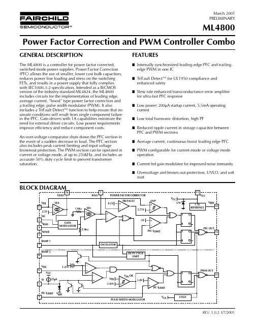
BLOCK DIAGRAM
Device
Package Operating Temp
IP102A 16DIP
IP102A 16SOP -40
OC ~ +85
OC ORDERING INFORMATION
16DIP
16SOP
元器件交易网www.cecb2b.com
IP102
Mar. 2004 Rev0
- 2 - WWW.INTERPIONSEMI.COM Dual OPAmp-Dual Comparator and Adj. Shunt Regulator
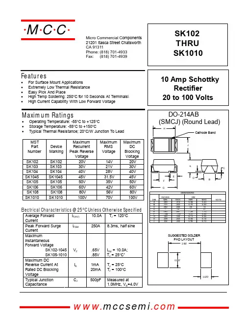
PIN DESCRIPTIONS
NO SYMBOL I/O DESCRIPTION
1 OUT1 O Comparator 1 Output
2 VIN1- I Comparator 1 Inverting Input
3 VIN1+ I Comparator 1 Non-Inverting Input
4 VCC - Positive Supply Voltage
5 VIN2+ I OP-Amp 1 Non-Inverting Input
6 VIN2-
I OP-Amp 1 Inverting Input
7 OUT2 O OP-Amp 1 Output
8 VREF - Adjustable Shunt Regulator Voltage Reference
9 IK I Adjustable Shunt Regulator Cathode
10 OUT3 O OP-Amp 2 Output
11 VIN3- I OP-Amp 2 Inverting Input
12 VIN3+ I OP-Amp 2 Non-Inverting Input
13 VEE - Negative Supply Voltage
14 VIN4+ I Comparator 2 Non-Inverting Input
15 VIN4- I Comparator 2 Inverting Input
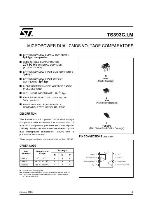
16 OUT4 O Comparator 2 Output PIN CONNECTIONS
VIN1+VIN1-OUT14
32113
VCC IP1029101112IK
8
765
VREF141516
VIN2+VIN2
-OUT2OUT3VIN3-VEEVIN
+VIN4+VIN4-
OUT4元器件交易网www.cecb2b.com
IP102
Mar. 2004 Rev0
- 3 -
WWW.INTERPIONSEMI.COM Dual OPAmp-Dual Comparator and Adj. Shunt Regulator
TOTAL SUPPLY VOLTAGE SECTION
CHARACTERISTICS SYMBOL CONDITIONS MIN TYP MAX UNIT
Total Supply Current Icc
0.8 1.5 mA Vee = 0V, No Load
Operational Amplifiers
Input Offset Voltage Vio
1 4.5 mV
Input Offset Current Iio
50 nA
Large Signal Voltage Gain Avd Vcc=15V, Vo=5~10V,
Rload =10K 60 100
dB
Supply Voltage Rejection
Ratio SVRR Vcc= 5V to 15V 65 100
dB
Common Mode Rejection
Ratio CMRR Vcc=15V,
Vicm=0~(Vcc)-1.8V 70 90
dB
Output Source Current Isource Vo=2.5V, Vid=+-1V 3 6
mA
Output Sink Current Isink Vo=2.5V,
Vid=+-1V 3 6
mA
Phase Margin PM Rload=10K,Cload=100pF
55
Degree
Output Voltage High Voh Vcc=15V, Rload=10K 12 13
V
Output Voltage Low Vol Rload=10K
100 150 mV
Slew Rate SR Vi=10V,
Vcc=12V,Rload=10K,Cloa
d=100pF 0.5 0.75
V/us
Gain Bandwidth GB Rload=10K,Cload=100pF,f
=100khz 1.0 1.5
MHz
Total Harmonic Distortion THD
0.05
% Input Bias Current Iib
50 150 nA PARAMETER SYMBOL VALUE UNIT
Supply Voltage Vcc 18 V
Operating temperature Topr -40 ~ +85
OC
Storage temperature Tstg -65 ~ 150
OC ABSOLUTE MAXIMUM RATINGS
ELECTRICAL CHARACTERISTICS
Ta = 25
OC, V
CC = 5V, V
EE = GND (unless otherwise specified. ) 元器件交易网www.cecb2b.com
IP102
Mar. 2004 Rev0
- 4 - WWW.INTERPIONSEMI.COM Dual OPAmp-Dual Comparator and Adj. Shunt Regulator
Comparators
CHARACTERISTICS SYMBOL CONDITIONS MIN TYP MAX UNIT
Input Offset Voltage Vio
5 mV
Input Offset Current Iio
50 nA
Input Bias Current Iib
200 nA
High Level Output Current Ioh Vid = +1V, Vcc=Vo=15V
0.1 1 uA
Large Signal Voltage Gain Avd Vcc+=15V, Rload =15K,
Vo=1V to 11V 200
V/mV
Low Level Output Voltage Vol Vid = -1V, Isc = 4mA
100 400 mV
Output Sink Current Isc Vid = -1V, Vo = 1.5V 6 16
mA
Input Common Mode
Voltage Range Vicm
0
(Vcc) -
1.5 V
Differential Input Voltage Vid
Vcc V
Adjustable Shunt Regulator
Cathode to Anode Voltage Vka
Vref
18 V
Cathode Current Ik
0.5
150 mA
Reference Input Voltage Vref IP102 2.475 2.5 2.525 V
Reference Input Voltage
Deviation dVref Vka=Vref, Ik=10mA
-40
OC < Ta <85
OC 7 30 mV
Load Regulation Rload Vka=Vref,Ik=10mA~100m
A
20 50 mV
Minimum Cathode Current
for Regulation Imin Vka = Vref
0.2 0.5 mA
Off-State Cathode Current Ioff Vka=18V, Vref=0V
0.1 1 uA ELECTRICAL CHARACTERISTICS
Ta = 25
OC, V
CC = 5V, V
EE=GND (unless otherwise specified. ) 元器件交易网www.cecb2b.com