SC1182资料
- 格式:pdf
- 大小:194.52 KB
- 文档页数:12
PROGRAMMABLE SYNCHRONOUS DC/DC
CONVERTER, DUAL LOW DROPOUT
REGULATOR CONTROLLER
© 1998 SEMTECH CORP.August 25, 1998
652 MITCHELL ROAD NEWBURY PARK CA 91320SC1182/3
1ORDERING INFORMATIONDESCRIPTION
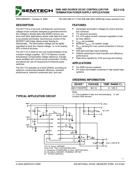
The SC1182/3 combines a synchronous voltage modecontroller with two low-dropout linear regulatorsproviding most of the circuitry necessary to implementthree DC/DC converters for powering advancedmicroprocessors such as Pentium® II (Klamath) orDeschutes.
The SC1182/3 switching section features an integrat-ed 5 bit D/A converter, pulse by pulse current limiting,integrated power good signaling, and logic compatibleshutdown. The SC1182/3 switching section operatesat a fixed frequency of 200kHz, providing an optimumcompromise between size, efficiency and cost in theintended application areas. The integrated D/A con-verter provides programmability of output voltagefrom 2.0V to 3.5V in 100mV increments and 1.30V to2.05V in 50mV increments with no external compo-nents.
The SC1182/3 linear sections are low dropout regula-tors. The SC1182 supplies 1.5V for GTL bus and 2.5Vfor non-GTL I/O.
For the SC1183 both LDO’s are adjustable.
Pentium is a registered trademark of Intel CorporationTEL:805-498-2111 FAX:805-498-3804 WEB:http://www.semtech.com
BLOCK DIAGRAM
2.5V/ADJ. 1.5V/ADJ. 1.265V FET CONTROLLER REF. FET CONTROLLER REF.
LDOV PIN CONFIGURATION
AGNDGATE1LDOS1LDOS2VCCOVPPWRGOODCS-CS+PGNDHDHPGNDL123LDOV
456789101112242322212019181716151413VOSENSEENBSTHBSTLDLVID0VID1VID2VID3VID4GATE2Top View
(24 Pin SOIC)FEATURES
• Synchronous design, enables no heatsink solution• 95% efficiency (switching section)• 5 bit DAC for output programmability• On chip power good function• Designed for Intel Pentium® ll VRM8.1 require-ments• 1.5V, 2.5V or Adj. @ 1% for linear section
APPLICATIONS
• Pentium® ll or Deschutes microprocessor supplies• Flexible motherboards• 1.3V to 3.5V microprocessor supplies• Programmable triple power supplies
Part Number(1)PackageLinearVoltageTemp.Range (TJ)
SC1182CSWSO-241.5V/2.5V0° to 125°C
SC1183CSWSO-24Adj.0° to 125°C
Note:(1) Add suffix ‘TR’ for tape and reel.元器件交易网www.cecb2b.comPROGRAMMABLE SYNCHRONOUS DC/DC
CONVERTER, DUAL LOW DROPOUT
REGULATOR CONTROLLER
© 1998 SEMTECH CORP.August 25, 1998
652 MITCHELL ROAD NEWBURY PARK CA 91320SC1182/3
2ParameterSymbolMaximumUnits
VCC to GNDVIN-0.3 to +7V
PGND to GND± 1V
BST to GND-0.3 to +15V
Operating Temperature RangeTA0 to +70°C
Junction Temperature RangeTJ0 to +125°C
Storage Temperature RangeTSTG-65 to +150°C
Lead Temperature (Soldering) 10 secondsTL300°C
Thermal Impedance Junction to AmbientθJA80°C/W
Thermal Impedance Junction to CaseθJC25°C/WABSOLUTE MAXIMUM RATINGS
ELECTRICAL CHARACTERISTICS
Unless specified: VCC = 4.75V to 5.25V; GND = PGND = 0V; VOSENSE = VO; 0mV < (CSp-CSm) < 60mV; LDOV = 11.4V to 12.6V; TA = 25°CPARAMETERCONDITIONSMINTYPMAXUNITS
Switching Section
Output VoltageIO = 2ASee Note 1.
Supply VoltageVCC4.27V
Supply CurrentVCC = 5.0815mA
Load RegulationIO = 0.8A to 15A1%
Line Regulation0.5%
Minimum operating voltage4.2V
Current Limit Voltage607080mV
Oscillator Frequency180200220kHz
Oscillator Max Duty Cycle9095%
Peak DH Sink/Source CurrentBSTH-DH = 4.5V, DH-PGNDH = 2V1A
Peak DL Sink/Source CurrentBSTL-DL = 4.5V, DL-PGNDL = 2V1A
Output Voltage Tempco30100ppm/oC
Gain (AOL)VOSENSE to VO35dB
OVP threshold voltage120%
OVP source currentVOVP = 3.0V10mA
Power good threshold voltage88112%
Dead time50100ns
Linear Sections
Quiescent currentLDOV = 12V5mA
Output Voltage (LDO1 SC1182)2.4752.5002.525V
Output Voltage (LDO2 SC1182)1.4851.5001.515V
Reference Voltage (SC1183)1.2521.2651.278V
Feedback Pin Bias Current (SC1183)10uA
Gain (AOL)LDOS (1,2) to GATE (1,2)90dB
Load RegulationIO = 0 to 8A(2)0.3%
Line Regulation0.3%
Output Impedance200Ω
Notes:(1) See Output Voltage table. (2) In application circuit.元器件交易网www.cecb2b.comPROGRAMMABLE SYNCHRONOUS DC/DCCONVERTER, DUAL LOW DROPOUT
REGULATOR CONTROLLER
© 1998 SEMTECH CORP.August 25, 1998
652 MITCHELL ROAD NEWBURY PARK CA 91320SC1182/3
3Note:(1) All logic level inputs and outputs are opencollector TTL compatible.PIN DESCRIPTION
PinPin NamePin Function1AGNDSmall Signal Analog and Digital Ground2GATE1Gate Drive Output LDO1
3LDOS1Sense Input for LDO1
4LDOS2Sense Input for LDO25VCCInput Voltage
6OVPHigh Signal out if VO>setpoint +20%
7PWRGOOD(1)Open collector logic output, high if VOwithin 10% of setpoint8CS-Current Sense Input (negative)9CS+Current Sense Input (positive)
10PGNDHPower Ground for High Side Switch11DHHigh Side Driver Output
12PGNDLPower Ground for Low Side Switch
13DLLow Side Driver Output14BSTLSupply for Low Side Driver
15BSTHSupply for High Side Driver16EN(1)Logic low shuts down the converter;High or open for normal operation.17VOSENSETop end of internal feedback chain