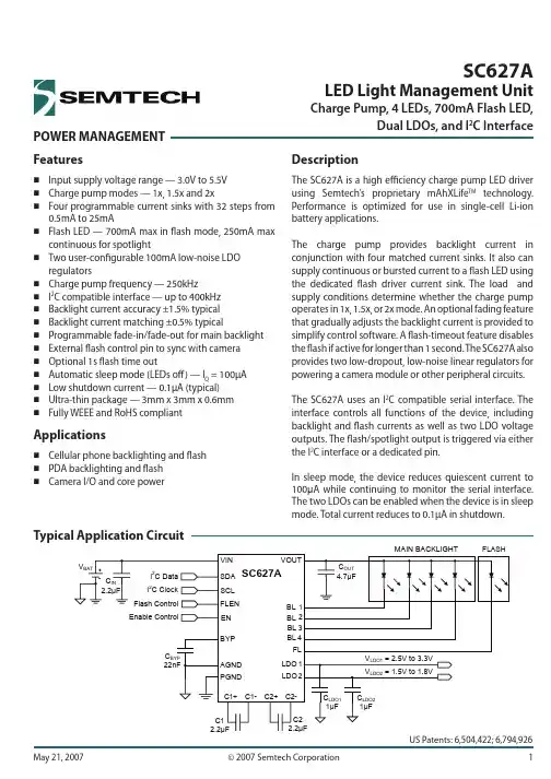
POWER MANAGEMENT SC627ALED Light Management UnitCharge Pump, 4 LEDs, 700mA Flash LED,Dual LDOs, and I 2C Interface FeaturesInput supply voltage range — 3.0V to 5.5V Charge pump modes — 1x, 1.5x and 2xFour programmable current sinks with 32 steps from 0.5mA to 25mAFlash LED — 700mA max in fl ash mode, 250mA max continuous for spotlight Two user-confi gurable 100mA low-noise LDO regulatorsCharge pump frequency — 250kHzI 2C compatible interface — up to 400kHz Backlight current accuracy ±1.5% typical Backlight current matching ±0.5% typicalProgrammable fade-in/fade-out for main backlight External fl ash control pin to sync with camera Optional 1s fl ash time outAutomatic sleep mode (LEDs off ) — I Q = 100μA Low shutdown current — 0.1μA (typical)Ultra-thin package — 3mm x 3mm x 0.6mm Fully WEEE and RoHS compliantApplicationsCellular phone backlighting and fl ashPDA backlighting and flash Camera I/O and core powerDescriptionThe SC627A is a high effi ciency charge pump LED driver using Semtech’s proprietary mAhXLife TM technology. Performance is optimized for use in single-cell Li-ion battery applications.The charge pump provides backlight current in conjunction with four matched current sinks. It also can supply continuous or bursted current to a fl ash LED using the dedicated fl ash driver current sink. The load and supply conditions determine whether the charge pump operates in 1x, 1.5x, or 2x mode. An optional fading feature that gradually adjusts the backlight current is provided to simplify control software. A fl ash-timeout feature disables the fl ash if active for longer than 1 second. T he SC627A also provides two low-dropout, low-noise linear regulators for powering a camera module or other peripheral circuits.The SC627A uses an I 2C compatible serial interface. The interface controls all functions of the device, including backlight and fl ash currents as well as two LDO voltage outputs. The fl ash/spotlight output is triggered via either the I 2C interface or a dedicated pin.In sleep mode, the device reduces quiescent current to 100μA while continuing to monitor the serial interface. The two LDOs can be enabled when the device is in sleep mode. Total current reduces to 0.1μA in shutdown.US Patents: 6,504,422; 6,794,926Typical Application CircuitPin Confi gurationMarking InformationOrdering InformationDevicePackageSC627AULTRT (1)(2)MLPQ-UT-20 3×3SC627AEVBEvaluation BoardNotes:(1) Available in tape and reel only. A reel contains 3,000 devices.(2) Available in lead-free package only. Device is WEEE and RoHScompliant.Exceeding the above specifi cations may result in permanent damage to the device or device malfunction. Operation outside of the parametersspecifi ed in the Electrical Characteristics section is not recommended.NOTES:(1) Tested according to JEDEC standard JESD22-A114-B.(2) Calculated from package in still air, mounted to 3” x 4.5”, 4 layer FR4 PCB with thermal vias under the exposed pad per JESD51 standards.Absolute Maximum RatingsVIN (V) . . . . . . . . . . . . . . . . . . . . . . . . . . . . . . . . . . . . -0.3 to +6.0VOUT (V) . . . . . . . . . . . . . . . . . . . . . . . . . . . . . . . . . . -0.3 to +6.0C1+, C2+ (V) . . . . . . . . . . . . . . . . . . . . . . . -0.3 to (V OUT + 0.3)Pin Voltage - All Other Pins (V) . . . . . . . . . . . -0.3 to (V IN + 0.3)VOUT Short Circuit Duration . . . . . . . . . . . . . . . . Continuous VLDO1, VLDO2, Short Circuit Duration . . . . . . Continuous ESD Protection Level (1)(kV) . . . . . . . . . . . . . . . . . . . . . . . . . . . . 2Recommended Operating ConditionsAmbient Temperature Range (°C) . . . . . . . . -40 < T A < +85VIN (V) . . . . . . . . . . . . . . . . . . . . . . . . . . . . . . . . . 3.0 < V IN < 5.5 VOUT (V) . . . . . . . . . . . . . . . . . . . . . . . . . . . . . . . 2.5 < V OUT < 5.25 Voltage Diff erence between any two LEDs (V) . . . . . . < 1.2Thermal InformationThermal Resistance, Junction to Ambient (2) (°C/W) . . . . 35Maximum Junction Temperature (°C) . . . . . . . . . . . . . . +150Storage Temperature Range (°C) . . . . . . . . . . . . -65 to +150Peak IR Reflow Temperature (10s to 30s) (°C) . . . . . . . +260Unless otherwise noted, T A = +25°C for Typ, -40ºC to +85°C for Min and Max, T J(MAX) = 125ºC, V IN = 3.0V to 4.2V, C IN = C 1= C 2= 2.2μF,C OUT = 4.7μF (ESR = 0.03Ω), ΔV F ≤ 1.2V (1)ParameterSymbol Conditions Min Typ Max UnitsSupply Specifi cations Shutdown CurrentI Q(OFF)Shutdown, V IN = 4.2V 0.12μATotal Quiescent CurrentI QSleep (LDOs off ), EN = V IN100160μASleep (LDOs on), EN = V IN ,V IN > (V LDO + 300mV), I LDO < 200mA220340Charge pump in 1x mode, 4 backlights on 3.8 4.65mACharge pump in 1.5x mode, 4 backlights on 4.6 5.85Charge pump in 2x mode, 4 backlights on4.65.85Fault Protection Output Short Circuit Current Limit I OUT(SC)VOUT pin shorted to GND300mA Over-Temperature T OTP 160°C Flash Mode Safety Timer (2)t FL(MAX)Flash sink active0.751.001.25sElectrical CharacteristicsParameterSymbol Conditions Min Typ Max UnitsFault Protection (continued)Charge PumpOver-Voltage ProtectionV OVP VOUT pin open circuit, V OUT = V OVPrising threshold5.35.76.0V Undervoltage LockoutV UVLO Decreasing V IN2.4V V UVLO-HYS300mVCharge Pump Electrical Specifi cations Maximum Total Output CurrentI OUT(MAX)V IN > 3.4V, sum of all active LED currents,V OUT(MAX) = 4.0V800mA Backlight Current Setting I BL Nominal setting for BL1 thru BL40.525mA Flash Current Setting I FL Nominal setting for FL 50700mA Backlight Current Accuracy I BL_ACC V IN = 3.7V, I BL = 12mA, T A = 25°C-8±1.5+8%Backlight Current Matching I BL-BL V IN = 3.7V, I BL = 12mA (3)-3.5±0.5+3.5%Flash Current Accuracy I FL_ACC V IN = 3.7V, I FL = 500mA, T A = 25°C -15+15%1x Mode to 1.5x Mode Falling Transition Voltage V TRANS1x I OUT = 40mA, I BLn = 10mA, V OUT = 3.2V 3.27V 1.5x Mode to 1x Mode HysteresisV HYST1x I OUT = 40mA, I BLn = 10mA, V OUT = 3.2V 250mV 1.5x Mode to 2x Mode Falling Transition Voltage V TRANS1.5x I OUT = 40mA, I BLn = 10mA, V OUT = 4.0V (4) 2.92V 2x Mode to 1.5x Mode HysteresisV HYST1.5x I OUT = 40mA, I BLn = 10mA, V OUT = 4.0V (4)300mV Current Sink Off -State Leakage Current I BLn V IN = V BLn = 4.2V 0.11μA Pump Frequencyf PUMPV IN = 3.2V250kHzLDO Electrical Specifi cations LDO1 Voltage Setting V LDO1Range of nominal settings in 100mV increments 2.5 3.3V LDO2 Voltage Setting V LDO2Range of nominal settings in 100mV increments 1.5 1.8V LDO1, LDO2 Output Voltage AccuracyV LDO1, V LDO2V IN = 3.7V, I LDO = 1mA -3.5±3+3.5%Line RegulationΔV LINELDO1, I LDO1 = 1mA, V OUT = 2.8V2.17.2mV LDO2, I LDO2 = 1mA, V OUT = 1.8V1.34.8Electrical Characteristics (continued)Electrical Characteristics (continued)Notes:(1) ΔV F is the voltage difference between any two LEDs.(2) Once tripped, fl ash output will remain disabled until FLEN pin is cycled or reset via serial interface.(3) Current matching equals ± [I BL(MAX) - I BL(MIN ] / [I BL(MAX) + I BL(MIN)].(4) Test voltage is V OUT = 4.0V — a relatively extreme LED voltage — to force a transition during test. Typically V OUT = 3.2V for white LEDs.(5) Dropout is defi ned as (V IN - V LDO1) when V LDO1 drops 100mV from nominal. Dropout does not apply to LDO2 since it has a maximum output voltageof 1.8V.(6)Guaranteed by designElectrical Characteristics (continued)Typical CharacteristicsBattery Current (4 LEDs) — 25mA Each1001101201301401501603.03.23.43.63.84.04.2V IN (V)B a t t e r yC u r r e n t (m A )V OUT =3.66V, I OUT =100mA, 25°CBacklight Effi ciency (4 LEDs) — 25mA Each50607080901003.03.23.43.63.84.04.2V IN (V)% E f f i c i e n c yV OUT =3.66V, I OUT =100mA, 25°CBacklight Effi ciency (4 LEDs) — 12mA EachV OUT =3.50V, I OUT =48mA, 25°C50607080901003.03.23.43.63.84.04.2V IN (V)% E f f i c i e n c yBacklight Effi ciency (4 LEDs) — 5.0mA Each50607080901003.03.23.43.63.84.04.2V IN (V)% E f f i c i e n c yV OUT =3.33V, I OUT =20mA, 25°CBattery Current (4 LEDs) — 5.0mA Each1520253035403.03.23.43.63.84.04.2V IN (V)B a t t e r yC u r r e n t (m A )V OUT =3.33V, I OUT =20mA, 25°CBattery Current (4 LEDs) — 12mA Each4552596673803.03.23.43.63.84.04.2V IN (V)B a t t e r yC u r r e n t (m A )V OUT =3.50V, I OUT =48mA, 25°CTypical Characteristics (continued)Flash Current — 700mA40050060070080090010003.03.23.43.63.84.04.2V IN (V)F l a s h C u r r e n t (m A )V OUT =3.49V at 25°CSpotlight Current — 50mA474849505152533.03.23.43.63.84.04.2V IN (V)S p o t l i g h t C u r r e n t (m A )V OUT =3.02V at 25°CFlash Current — 400mA3103403704004304604903.03.23.43.63.84.04.2V IN (V)F l a s h C u r r e n t (m A )V OUT =3.39V at 25°CSpotlight Current — 250mA1601902202502803103403.03.23.43.63.84.04.2V IN (V)S p o t l i g h t C u r r e n t (m A )V OUT =3.50V at 25°CPSRR vs. Frequency (LDO2)-70-60-50-40-30-20-10010100100010000Frequency (Hz)P S R R (d B )V IN =3.7V at 25°C, I LDO2=50mA, V LDO2=1.8VPSRR vs. Frequency (LDO1)-70-60-50-40-30-20-10010100100010000Frequency (Hz)P S R R (d B )V IN =3.7V at 25°C, I LDO1=50mA, V LDO1=2.8VTypical Characteristics (continued)Load Regulation (LDO1)-24-16-8081624306090120150I LDO1(mA)O u t p u t V o l t a g e V a r i a t i o n (m V )V LDO1=3.3V, V IN =3.7V, 25°CNoise vs Load Current (LDO1)5060708090100020406080100I LDO1 (mA)N o i s e (μV )V LDO1=2.8V, V IN =3.7V, 25°CLoad Regulation (LDO2)-24-16-8816240306090120150I LDO2(mA)O u t p u t V o l t a g e V a r i a t i o n (m V )V LDO2=1.8V, V IN =3.7V, 25°CNoise vs Load Current (LDO2)20406080100020406080100I LDO2 (mA)N o i s e (μV )V LDO2=1.8V, V IN =3.7V, 25°CLine Regulation (LDO1)-3-2-1123.03.23.43.63.84.04.2V IN (V)O u t p u t V o l t a g e V a r i a t i o n (m V )V LDO1=2.8V, I LDO1=1mA, 25°CLine Regulation (LDO2)-3-2-1123.03.23.43.63.84.04.2V IN (V)O u t p u t V o l t a g e V a r i a t i o n (m V )V LDO2=1.8V, I LDO2=1mA, 25°CTypical Characteristics (continued)Load Transient Response (LDO2) — Falling EdgeTime (200μs/div)V LDO2 (50mV/div)I LDO2(100mA/div)V IN =3.7V, V LDO2=1.8V, I LDO2=100 to 1mALoad Transient Response (LDO1) — Rising EdgeTime (20μs/div)V LDO1 (50mV/div)I LDO1 (100mA/div)V IN =3.7V, V LDO1=2.8V, I LDO1=1 to 100mATime (200μs/div)Load Transient Response (LDO1) — Falling EdgeV IN =3.7V, V LDO1=2.8V, I LDO1=100 to 1mAV LDO1 (50mV/div)I LDO1 (100mA/div)Time (20μs/div)Load Transient Response (LDO2) — Rising EdgeV IN =3.7V, V LDO2=1.8V, I LDO2=1 to 100mAV LDO2 (50mV/div)I LDO2 (100mA/div)Typical Characteristics (continued)Output Short Circuit Current LimitTime (1ms/div)V OUT (1V/div)I OUT (100mA/div)V OUT =0V, V IN =4.2V, 25°CFlash Mode Safety TimerTime (200ms/div)V FLEN (5V/div)V OUT (2V/div)I FL (200mA/div)V IN =3.7V, 25°COutput Open Circuit ProtectionTime (200μs/div)V BL1 (500mV/div)V OUT (2V/div)I BL1 (20mA/div)V IN =3.7V, 25°CFlash Current PulseV FLEN (5V/div)V OUT (2V/div)I FL(200mA/div)I FL =400mA, V IN =3.7V, V OUT =3.7V, 25°CTime (40ms/div)Pin DescriptionsPin #Pin Name Pin Function1C2-Negative connection to bucket capacitor 2 — requires a 2.2μF capacitor connected to C2+2PGND Ground pin for high current charge pump and Flash LED driver3FL Current sink output for fl ash LED(s)4BL1Current sink output for main backlight LED 1 — leave this pin open if unused 5BL2Current sink output for main backlight LED 2 — leave this pin open if unused 6BL3Current sink output for main backlight LED 3 — leave this pin open if unused 7BL4Current sink output for main backlight LED 4 — leave this pin open if unused 8AGND Analog ground pin — connect to ground and separate from PGND current 9SCL I2C clock input pin10FLEN Control pin for fl ash LED(s) — high = ON, low = OFF11SDA I2C bi-directional data pin — used for read and write operations for all internal registers (refer to Register Map and I2C Interface sections)12EN Chip enable — active high — low state resets all registers (see register map table) 13BYP Bypass pin for voltage reference — connect with a 22nF capacitor to AGND14LDO2Output of LDO2 — connect with a 1μF capacitor to AGND15LDO1Output of LDO1 — connect with a 1μF capacitor to AGND16VOUT Charge pump output — all LED anode pins should be connected to this pin — requires a 4.7μF capacitor to PGND17C2+Positive connection to bucket capacitor 2 — requires a 2.2μF capacitor connected to C2-18C1+Positive connection to bucket capacitor 1 — requires a 2.2μF capacitor connected to C1-19VIN Battery voltage input — connect with a 2.2μF capacitor to PGND20C1-Negative connection to bucket capacitor 1 — requires a 2.2μF capacitor connected to C1+T THERMAL PAD Thermal pad for heatsinking purposes — connect to ground plane using multiple vias — not connected internallyBlock DiagramC1+C1-C2+C2-VOUT BL1BL2BL3BL4FLVIN EN FLEN PGNDLDO2LDO1AGNDBYP SCLSDAGeneral DescriptionThis design is optimized for handheld applications supplied from a single Li-Ion cell and includes the following key features:A high effi ciency fractional charge pump that supplies power to all LEDsFour matched current sinks that control LED backlighting current, with 0.5mA to 25mA per LEDAn LED fl ash output that provides up to 700mA of momentary current or up to 250mA of continuous spotlight currentTwo adjustable LDOs with outputs ranging from 2.5V to 3.3V for LDO1 and 1.5V to 1.8V for LDO2, adjustable in 100mV incrementsAn I 2C compatible interface that provides control of all device functionsHigh Current Fractional Charge PumpThe backlight and fl ash outputs are supported by a high effi ciency, high current fractional charge pump output at the VOUT pin. The charge pump multiplies the input voltage by 1, 1.5, or 2 times. The charge pump switches at a fi xed frequency of 250kHz in 1.5x and 2x modes and is disabled in 1x mode to save power and improve effi ciency.The mode selection circuit automatically selects the 1x, 1.5x or 2x mode based on circuit conditions. Circuit conditions such as low input voltage, high output current, or high LED voltage place a higher demand on the charge pump output. A higher numerical mode may be needed momentarily to maintain regulation at the VOUT pin during intervals of high demand, such as the high current of an LED fl ash or the droop at the VIN pin during a supply voltage transient. The charge pump responds to these momentary high demands, setting the charge pump to the optimum mode (1x, 1.5x or 2x), as needed to deliver the output voltage and load current while optimizing effi ciency. Hysteresis is provided to prevent mode toggling.The charge pump requires two bucket capacitors for low ripple operation. One capacitor must be connected•••••between the C1+ and C1- pins and the other must be connected between the C2+ and C2- pins as shown in the typical application circuit diagram. These capacitors should be equal in value, with a minimum capacitance of 2.2μF to support the charge pump current requirements. The device also requires a 2.2μF capacitor on the VIN pin and a 4.7μF capacitor on the VOUT pin to minimize noise and support the output drive requirements. Capacitors with X7R or X5R ceramic dielectric are strongly recommended for their low ESR and superior temperature and voltage characteristics. Y5V capacitors should not be used as their temperature coeffi cients make them unsuitable for this application.LED Backlight Current SinksThe backlight current is set via the I 2C compatible interface. The current is regulated to one of 32 values between 0.5mA and 25mA. T he step size varies depending upon the current setting. Between 0.5mA and 12mA, the step size is 0.5mA. The step size increases to 1mA for settings between 12mA and 15mA and 2mA for settings greater than 15mA. This feature allows fi ner adjustment for dimming functions in the low current setting range and coarse adjustment at higher current settings where small current changes are not visibly noticeable in LED brightness.All backlight current sinks have matched currents, even when there is variation in the forward voltages (ΔV F ) of the LEDs. A ΔV F of 1.2V is supported when the input voltage is at 3.0V. Higher ΔV F LED mis-match is supported when V IN is higher than 3.0V. All current sink outputs are compared and the lowest output is used for setting the voltage regulation at the VOUT pin. This is done to ensure that suffi cient bias exists for all LEDs, including the fl ash LED.The backlight LEDs default to the off state upon power-up. For backlight applications using less than four LEDs, any unused output must be left open and the unused LED driver must remain disabled. When writing to the Backlight Enable Control register, a zero (0) must be written to the corresponding bit of any unused output.Applications InformationApplications Information (continued)Backlight Quiescent CurrentThe quiescent current required to operate all four backlights is reduced by 1.5mA when backlight current is set to 4.0mA or less. This feature results in higher effi ciency under light-load conditions. Further reduction in quiescent current will result from using fewer than four LEDs.Fade-In and Fade-OutBacklight brightness can be set to automatically fade-in when current is set to increase and fade-out when current is set to decrease. When enabled with a new current setting, the current will step through each incremental setting between the old and new values. The result is a visually smooth change in brightness with a rate of fade that can be set to 8, 16, 24, or 32 ms per step.LED Flash and Spotlight Current SinkA single output current sink is provided to drive both fl ash and spotlight functions. In fl ash mode, this current sink provides up to 700mA for a fl ash LED or array of parallel LEDs . Flash current settings are in 50mA increments from 50mA to 700mA. The FLEN pin directly triggers the FLASH function when pulled high, or it can be wired to VIN to enable software control via the serial interface.In spotlight mode, the output can be set for up to 250mA of continuous current. Settings are available in 50mA increments from 50mA to 250mA. Continuous operation above 250mA is not recommended due to high power dissipation.Flash and Spotlight Safety TimerA safety timer disables the fl ash and spotlight output current sink if the sink remains active for an extended period. The timer protects the SC627A and the LED from high power dissipation that can cause overheating. The timer’s default state is on, but the timer may be disabled via the serial interface to allow continuous output current in spotlight mode. The safety timer aff ects only the FL pin and will turn off the sink after a period of 1 second. Thetimer may be reset by either forcing the FLEN pin low or by resetting the Flash/Spotlight control bits via the interface.Programmable LDO OutputsTwo low dropout (LDO) regulators are provided for camera module I/O and core power. Each LDO has at least 100mA of available load current with ±3.5% accuracy. The minimum current limit is 200mA, so outputs greater than 100mA are possible at somewhat reduced accuracy.A 1μF, low ESR capacitor should be used as a bypass capacitor on each LDO output to reduce noise and ensure stability. In addition, it is recommended that a minimum 22nF capacitor be connected from the BYP pin to ground to minimize noise and achieve optimum power supply rejection. A larger capacitor can be used for this function, but at the expense of increasing turn-on time. Capacitors with X7R or X5R ceramic dielectric are strongly recommended for their low ESR and superior temperature and voltage characteristics. Y5V capacitors should not be used as their temperature coeffi cients make them unsuitable for this application.Shutdown StateThe device is disabled when the EN pin is low. All registers are reset to default condition when EN is low.Sleep ModeWhen all LEDs are off , sleep mode is activated. This is a reduced current mode that helps minimize overall current consumption by turning off the clock and the charge pump while continuing to monitor the serial interface for commands. Both LDOs can be powered up while in sleep mode.I 2C Compatible Interface FunctionsAll device functions can be controlled via the I 2Ccompatible interface. The interface is described in detail in the Serial I nterface section of the datasheet.Protection FeaturesThe SC627A provides several protection features to safeguard the device from catastrophic failures. These features include:Output Open Circuit ProtectionOver-Temperature ProtectionCharge Pump Output Current LimitLDO Current LimitLED Float DetectionOutput Open Circuit ProtectionOver-Voltage Protection (OVP) is provided at the VOUT pin to prevent the charge pump from producing an excessively high output voltage. In the event of an open circuit at VOUT, the charge pump runs in open loop and the voltage rises up to the OVP limit. OVP operation ishysteretic, meaning the charge pump will momentarily turn off until V OUT is suffi ciently reduced. The maximum OVP threshold is 6.0V, allowing the use of a ceramic output capacitor rated at 6.3V with no fear of over-voltage damage.Over-Temperature ProtectionThe Over-Temperature (OT) protection circuit helps prevent the device from overheating and experiencing a catastrophic failure. When the junction temperature exceeds 160 °C, the device goes into thermal shutdown with all outputs disabled until the junction temperature is reduced. All register information is retained during thermal shutdown.•••••Applications Information (continued)Charge Pump Output Current LimitThe device also limits the charge pump current at the VOUT pin. When VOUT is shorted to ground, the typicaloutput current is 300mA. The current limiting is triggered by an output under-voltage lockout below 2V. The output returns to normal when the short is removed and VOUT is above 2.5V. Above 2.5V, a typical current limit of 300mA applies when the FL current sink is off and a typical current limit of 1A applies when the FL current sink is on.LDO Current LimitThe device limits the output currents of LDO1 and LDO2 to help prevent it from overheating and to protect the loads. The minimum limit is 200mA, so load current greater than the rated 100mA can be used with degraded accuracy and larger dropout without tripping the current limit.LED Float Detection Float detect is a fault detection feature of the LED current sink outputs. If an output is programmed to be enabled and an open circuit fault occurs at any current sink output,that output will be disabled to prevent a sustained output OVP condition from occurring due to the resulting open loop. Float detect ensures device protection but does not ensure optimum performance. Unused LED outputs must be disabled to prevent an open circuit fault from occurring.PCB Layout ConsiderationsThe layout diagram in Figure 1 illustrates a proper two-layer PCB layout for the SC627A and supporting components. Following fundamental layout rules is critical for achieving the performance specifi ed in the Electrical Characteristics table. The following guidelines are recommended when developing a PCB layout:Place all bypass and decoupling capacitors — C1, C2, CIN, COUT, CLDO1, CLDO2, and CBYP as close to the device as possible.All charge pump current passes through VIN, VOUT, and the bucket capacitor connection pins. Ensure that all connections to these pins make use of wide traces so that the resistive drop on each connection is minimized.The thermal pad should be connected to the ground plane using multiple vias to ensure proper thermal connection for optimal heat transfer.•••Applications Information (continued)Make all ground connections to a solid ground plane as shown in the example layout (Figure 3).If a ground layer is not feasible, the following groupings should be connected:P GND — CIN, COUT A GND — Ground Pad, CLDO1, CLDO2, CBYPIf no ground plane is available, PG ND and AG ND should be routed back to the negative battery terminal as separate signals using thick traces. Joining the two ground returns at the terminal prevents large pulsed return currents from mixing with the low-noise return currents of the LDOs.Both LDO output traces should be made as wide as possible to minimize resistive losses.••••Figure 1 — Recommended PCB LayoutFigure 2 — Layer 1Figure 3 — Layer 2Register MapAddressD7D6D5D4D3D2D1D0Reset ValueDescription0x00FADE_1FADE_0FADE_EN BL_4BL_3BL_2BL_1BL_00x00Backlight Current Control 0x010(1)0(1)0(1)0(1)BLEN_4BLEN_3BLEN_2BLEN_10x00Backlight Enable Control 0x020(1)0(1)0(1)FLTO FL_2FL_1FL_0FL/SPLB 0x10Flash/SpotlightControl 0x030(1)LDO2_2LDO2_1LDO2_0LDO1_3LDO1_2LDO1_1LDO1_00x00LDO ControlNotes:(1) 0 = always write a 0 to these bitsRegister and Bit Defi nitionsBacklight Current Control Register (0x00)This register is used to set the currents for the backlight current sinks, as well as to enable and set the fade step rate. These current sinks need to be enabled in the Backlight Enable Control register to be active.FADE[1:0]These bits are used to set the rise/fall rate between two backlight currents as follows:FADE_1FADE_0Fade Feature Rise/Fall Rate (ms/step)0032 01241016118The number of steps in changing the backlight current will be equal to the change in binary count of bits BL[4:0].FADE_ENThis bit is used to enable or disable the fade feature. When the fade function is enabled and a new backlight current is set, the backlight current will change from its currentvalue to a new value set by bits BL[4:0] at a rate of 8ms to 32ms per step. A new backlight level cannot be written during an ongoing fade operation, but an ongoing fade operation may be cancelled by resetting the fade bit. Clearing the fade bit during an ongoing fade operation changes the backlight current immediately to the value of BL[4:0]. The number of counts to complete a fade operation equals the diff erence between the old and new backlight values to increment or decrement the BL[4:0] bits. If the fade bit is cleared, the current level will change immediately without the fade delay. The rate of fade may be changed dynamically, even while a fade operation is active, by writing new values to the FADE_1 and FADE_0 bits. The total fade time is determined by the number of steps between old and new backlight values, multiplied by the rate of fade in ms/step. The longest elapsed time for a full scale fade-out of the backlight is nominally 1.024 seconds when the default interval of 32ms is used.。