第二讲:Lattice公司的isp1016芯片
- 格式:ppt
- 大小:134.00 KB
- 文档页数:13
PRODUCT SELECTOR GUIDE2012FPGA • CPLD • MIXED SIGNAL • INTELLECTUAL PROPERTY • DEVELOPMENT KITS • DESIGN TOOLSCONTENTS■A dvanced Packaging (4)■F PGA Products (6)■CPLD Products (8)■Power Management and Clock Management Products (8)■Intellectual Property and Reference Designs (10)■Development Kits and Evaluation Boards (14)■P rogramming Hardware (18)■FPGA and CPLD Design Software (19)■PAC-Designer® Design Software (19)Page 2Affordable InnovationLattice Semiconductor is committed to delivering value through innovative low cost, low power solutions.We’re innovating every day to drive down costs and deliver greater value. From cost sensitive consumerelectronics to leading edge communications equipment, designers are using Lattice products in a growingnumber of applications. We’ve shipped over a billion devices to customers worldwide and we understandthat we must deliver cost effective solutions and excellent service in order to succeed.Low Density and Ultra-Low Density FPGAsWe are committed to providing design engineers with the low cost and low power solutions they needto implement their designs quickly, easily and affordably. Lattice FPGA solutions offer unique features,low power, and excellent value for FPGA designs. Our low density LatticeECP3™ family is comprisedof the lowest power, SERDES-enabled FPGAs in the market today, and is ideally suited for deploymentin high volume cost- and power-sensitive wireless and wireline infrastructure, video camera and displayapplications. Our ultra-low density, low cost and low power iCE40™ and MachXO2™ FPGA familiesare ideal for applications ranging from glue logic and bridging to instant-on system control and flexibleI/O expansion. From mobile handsets to leading-edge telecommunications infrastructure, Lattice offerssolutions that minimize cost and power while maximizing value.Power Management and Clock ManagementOur Platform Manager™, Power Manager II and ispClock™ mixed signal product families feature acombination of programmable logic and programmable analog circuitry that allows system designersto reduce system cost and design time. These innovative products provide a fast and easy solution forintegrating a wide range of power and clock management functions within a single integrated circuit. Theseproducts can replace numerous discrete components, reducing cost and conserving board space, whileproviding users with additional design flexibility and time-to-market benefits.Software and Intellectual PropertyOur Lattice Diamond® development tool suite, iCEcube2™ design software, PAC-Designer software, and IPcore program allow design engineers to easily customize our devices for their unique system requirements.Lattice Diamond software tools enable users to synthesize a design, perform analysis, debug, anddownload a logic configuration to our FPGA devices, while iCEcube2 software supports our iCE40 family ofFGPAs. PAC-Designer software is used in the design of our mixed signal products.Our IP core program, LatticeCORE™, provides pre-tested, reusable functions, allowing designers to focuson their unique system architectures. These IP cores provide industry-standard functions including PCIExpress, DDR, Ethernet, CPRI, Serial RapidIO 2.1, SPI4, and embedded microprocessors. In addition, anumber of independent IP providers have teamed with Lattice to offer additional high quality, reusable IPcores. Partners are selected for their industry leadership, high development standards, and commitment tocustomer support.Page 3Page 4Organic Flip Chip BGAFine Pitch BGA1704-BallOrganic fcBGA 42.5 x 42.5 mm 3.25 mm height 1.00 mm pitch1020-BallOrganic fcBGA Revision 233 x 33 mm 3.25 mm height 1.00 mm pitch1152-Ball fpBGA 1156-Ball fpBGA 35 x 35 mm 2.60 mm height 1.00 mm pitc h900-Ball fpBGA 31 x 31 mm 2.60 mm height 1.00 mm pitch672-Ball fpBGA 27 x 27 mm 2.60 mm height 1.00 mm pitch484-Ball fpBGA 23 x 23 mm 2.60 mm height 1.00 mm pitch324-Ball ftBGA 19 x 19 mm 1.70 mm height 1.00 mm pitch256-Ball ftBGA 17 x 17 mmOption 1: 1.55 mm height Option 2: 2.10 mm height Option 3: 1.70 mm height 1.00 mm pitch 256-Ball caBGA 14 x 14 mm 1.70 mm height 0.80 mm pitch332-Ball caBGA 17 x 17 mm 2.00 mm height 0.80 mm pitch208-Ball ftBGA 17 x 17 mm 1.55 mm height 1.00 mm pitch256-Ball fpBGA 17 x 17 mm 2.10 mm height1.00 mm pitchFine Pitch BGAChip Array BGANote: Packages shown actual size. Height specification is max.Page 5208-Pin PQFP 28 x 28 mm (body)4.10 mm height 0.50 mm pitch176-Pin TQFP 24 x 24 mm (body)1.60 mm height 0.50 mm pitch144-Pin TQFP 20 x 20 mm (body)1.60 mm height 0.50 mm pitch100-Pin VQFP 14 x 14 mm (body)1.2 mm height 0.50 mm pitch100-Pin TQFP 128-Pin TQFP 14 x 14 mm (body)1.6 mm height0.50 mm pitch (100 TQFP)0.40 mm pitch (128 TQFP )44-Pin TQFP10 x 10 mm (body)1.20 mm height 1.60 mm height 0.80 mm pitch 48-Pin TQFP 7 x 7 mm (body)1.20 mm height 1.60 mm height0.50 mm pitchVQFP/TQFP/PQFP64-Pin QFNS 9 x 9 mm1.00 mm height 0.50 mm pitch 100-Ball csBGA 8 x 8 mm1.35 mm height 0.50 mm pitch132-Ball csBG A 8 x 8 mmOption 1: 1.35 mm heightOption 2: 1.00 mm height (iCE40)0.50 mm pitch 184-Ball csBG A 8 x 8 mm1.35 mm height 0.50 mm pitch284-Ball csBGA 12 x 12 mm 1.00 mm height 0.50 mm pitch 328-Ball csBGA 10 x 10 mm 1.50 mm height 0.50 mm pitch 132-Ball ucBGA 6 x 6 mm1.00 mm height 0.40 mm pitch 25-Ball WLCSP2.5 x 2.5 mm 0.62 mm height 0.40 mm pitch84-Pin QFNS 7 x 7 mm1.00 mm height 0.50 mm pitch 48-Pin QFNS 7 x 7 mm1.00 mm height 0.50 mm pitch144-Ball csBGA 7 x 7 mm1.10 mm height 0.50 mm pitch 64-Ball ucBGA 4 x 4 mm1.00 mm height 0.40 mm pitch 32-Pin QFNS 5 x 5 mm1.00 mm height 0.50 mm pitch 32-Pin QFN 5 x 5 mm0.60 mm height 0.50 mm pitch 56-Ball csBGA 6 x 6 mm1.35 mm height 0.50 mm pitch 81-Ball csBGA 5 x 5 mm1.00 mm height 0.50 mm pitch 225-Ball ucBGA 7 x 7 mm1.00 mm height 0.40 mm pitch 24-Pin QFNS 4 x 4 mm1.00 mm height 0.50 mm pitch64-Ball csBGA 5 x 5 mm1.10 mm height 0.50 mm pitch121-Ball csBGA 6 x 6 mm1.00 mm height 0.50 mm pitch 121-Ball ucBGA 5 x 5 mm1.00 mm height 0.40 mm pitch 81-Ball ucBGA 4 x 4 mm1.00 mm height 0.40 mm pitch 49-Ball ucBGA 3 x 3 mm1.00 mm height 0.40 mm pitch 36-Ball ucBGA2.5 x 2.5 mm 1.00 mm height0.40 mm pitchQFNS / QFNChip Scale BGAUltra Chip Scale BGAWafer Level Chip ScaleNote: Packages shown actual size. Height specification is max.NEWiCE40™Page 6Page 71) Pb-free only.ispClock ProductsPage 8Platform Manager and Power Manager II Device Selector Guide* ispPAC-POWR1014A OnlyPage 9LatticeCORE IP CoresThe following is a partial listing of LatticeCORE IP, for a complete listing of IP cores from Lattice and its 3rd party partners, please go to /ip.1. LatticeSCM™ MACO®-based IP cores are not included in this table.Page 10IP SuitesLattice IP Suites provide many of the functions required to develop a total solution for common FPGA applications. In addition, multipleLattice FPGA families are supported with each IP Suite, so designers can develop solutions across multiple Lattice families, taking advantage of the best features of each. The following table summarizes which IP cores are included in each IP Suite, and which FPGA families are supported.Page 11Page 12Page 13Page 14Features- Power connections and power sources - ispVM™ programming support- On-board and external reference clock sources• Available on Windows and Linux platforms • Software and IP with a 60-day license (Windows or Linux)• Variety of demos • USB download cable• Comprehensive Image Processing IP Library • On-board Broadcom ® Broadreach™ PHY Enables IP over Coax• On-board FTDI Chip provides easy programming via low cost USB cable- Gigabit Ethernet MAC Demo using Mico32- DDR3 Memory Controller Demo• Available on Windows and Linux platforms • USB A to USB B (Mini) Cable for FPGA Programming via a PC• 12V AC Power Adapter and International Plug Adapters•QuickSTART GuideFeaturesFeaturesFeaturesLatticeECP3 Versa Development KitHDR-60 Video Camera Development KitLatticeECP3 PCI Express Development KitLatticeXP2 Brevia2 Development Kit• LatticeECP3 PCI Express x1/x4 Solutions Board- PCI Express x1 and x4 edge connector interfaces- On-board Boot Flash- Both Serial SPI Flash and Parallel Flash via MachXO programming bridge - Shows interoperation with a highperformance DDR2 memory component - Switches, LEDs, displays for demo purposes- Input connection for lab-power supply• FPGA-based Image Signal Processing• Fully Production-Ready HDR Camera Design • 1080p Capable @ 60 frames per second• Supports up to 16 Megapixel Sensors • Supports up to two sensors simultaneously • Full 60fps in streaming mode needs no external frame buffer• Fast Auto Exposure Instantly Adjust to Changing Light• Greater than 120 dB High Dynamic Range (HDR) Performance• Direct HDMI/DVI output from FPGA • Extremely Low-Latency• The LatticeECP3 Versa Evaluation Board:- PCI Express 1.1 x1 Edge Connector Interface- Two Gigabit Ethernet Ports (RJ45)- 4 SMA Connectors for SERDES Access - USB Mini for FPGA Programming- LatticeECP3 FPGA: LFE3-35EA-FF484- 64 Mbit Serial Flash memory - 1 Gbit DDR3 Memory- 14-segment alpha-numeric display - Switches and LEDs for demos - SERDES Eye Quality Demo - 4 PCI Express Demos• LatticeXP2 FPGA: LFXP2-5E-6TN144C • 2 Mbit SPI Flash Memory • 1 Mbit SRAM• Programmed via included mini-USB Cable • 2x20 and 2x5 Expansion Headers• Push buttons for General Purpose I/O and Reset• 4-bit DIP Switch for user-defined inputs • 8 Status LEDs for user-defined outputsDevelop PCIe-based platforms using a low-cost, low-power SERDES-basedFPGA with proprietary and Lattice provided designs.A fully production ready High Dynamic Range (HDR) camera, designed to fit into commercially available camera housings. Supports full 1080p resolution at 60 frames per second in streaming mode through the FPGA, without the need for an external frame buffer.Industry’s lowest cost platform for design-ing PCI Express and Gigabit Ethernet based systems. The kit includes free demos and reference designs.Easy-to-use, low-cost platform for evaluat-ing and designing with LatticeXP2 FPGAs.Page 15FeaturesFeaturesiCEblink40 Evaluation KitMachXO2 Pico Development KitMachXO2 Control Development Kit• Two versions:- High Performance: iCE40HX1K-VQ100 - Low Power: iCE40LP1K-QN84• Powered by USB input• 1Mbit SPI PROM (enough for two iCE40HX1K images using WarmBoot)• Four capacitive-touch buttons (requires FPGA logic)• Four user LEDs• Dual PMOD header compatible with Digilent PMOD boards (6x2 header)• MachXO2 LCMXO2-1200ZE• 4-character 16-segment LCD display • 4 capacitive touch sense buttons • 1 Mbit SPI Flash• I 2C temperature sensor• Current and voltage sensor circuits • Expansion header for JTAG, I 2C• Standard USB cable for device programming and I 2C communication• RS-232/USB & JTAG/USB interface• RoHS-compliant packaging and process• MachXO2 LCMXO2-4000HC• Power Manager II ispPAC-POWR1014A • 128Mbit LPDDR memory, 4Mbit SPI Flash • Current and voltage sensor circuits • SD memory card socket • Microphone• Audio Amplifier and Delta-Sigma ADC• Up to two DVI sources and one DVI output.• Up to two Display Inputs (7:1 LVDS) and one Display Output (7:1 LVDS)• Audio output channel• Expansion header for JTAG, SPI, I 2C and PLD I/Os.• 3.33 MHz oscillator (can be modified to support 33.33 MHz or 333 kHz)• 1.2V and 3.3V power supplies• All iCE40HX1K I/O available on headers or 0.1” through-holes• Watch battery• QuickSTART Guide• LEDs & switches• Standard USB cable for device programming • RS-232/USB & JTAG/USB interface• RoHS-compliant packaging and process • AC adapter (international plugs)• QuickSTART Guide31, 2012. Standard list price: $39.MachXO Control Development Kit FeaturesMachXO Pico Dev. Kit & MachXO Control Dev. Kit• Preloaded Control SoC Demo • MachXO LCMXO2280• Power Manager II ispPAC-POWR1014A• 2Mbit SPI Flash & 1Mbit SRAM • I 2C temperature sensor • Current and voltage sensor circuits • On-board fan • Interface to 16 x 2 LCD panel*• SD memory and Compact Flash memory card sockets*• Audio output channel• Expansion header for SPI & I 2C • LEDs & switches• Standard USB cable for device programming and I 2C communication • RS-232/USB & JTAG/USB interface • 3” x 1” prototyping area • RoHS-compliant packaging and process * LCD panel and SD/Compact Flash memory not included in the development kit MachXO Mini Development Kit Features• MachXO PLD: LCMXO2280C-4TN144C• 2 Mbit SPI Flash memory • 1 Mbit SRAM• I 2C temperature sensor • USB mini jack sockets for power, JTAG programming, and RS-232 debugging • 2X16 header for off-board expansion provides access to top and right side MachXO banks• Push-buttons for sleep mode and reset• 4-bit DIP switch to user-defined inputs • ADC/DAC circuit • Sleep circuit• 8 LEDs for user-defined outputs• RoHS-compliant packaging and process• Two USB connector cables • QuickSTART GuidePage 16FeaturesFeaturesFeaturesPower Manager II Hercules Development KitProcessorPM Development KitPlatform Manager Development Kit• The Standard Edition Hercules DevelopmentKit features the following:- Preloaded Board Digital ManagementDemo- Hercules Standard Edition eval board- Power Manager II ispPAC-POWR1220AT8 and MachXOLCMXO2280 PLD• The Advanced Edition Hercules DevelopmentKit features the following:- Preloaded Board Digital ManagementDemo- Hercules Advanced Edition evaluationboard with CompactPCI headers- Power Manager II ispPAC-POWR1220AT8 and MachXOLCMXO2280 PLD- Backplane accessory evaluation boardand power supply for live hot-swap• AC adapter (international plugs)• USB Connector Cable• RoHS-compliant packaging and process• Pre-configured Processor Support Demo• ProcessorPM-POWR605• Power Manager II POWR6AT6• 3.3V, 2.5V, and 1.8V supply rails• LEDs• Slide potentiometer• 2x14 expansion header• USB mini jack socket (program/power)• 2 Push-Buttons• Preloaded Power Management Demo• LPTM10-12107, Platform Manager, 208-ballftBGA package• 35mm slide pots to emulate supply railvariations• Pads for user I/O, LED, and switches• JTAG and I2C interface headers• USB Cable• 4-Bit DIP Switch• JTAG and I2C Header Landings• RoHS-compliant packaging and process• USB connector cable• QuickSTART Guide• AC adapter with international plugs• Programmable with ispVM System software• QuickSTART GuideVersatile, ready to use hardware platformsfor evaluating and designing with PowerManager II devices. A Standard and Ad-vanced Edition of each kit is available.Versatile, ready-to-use hardware platformfor evaluating and designing with Proces-sorPM power management devices.A versatile, ready-to-use hardware plat-form for evaluating and designing withPlatform Manager devices.Features:Breakout Board Evaluation Kits•Preprogrammed with hardware test programLCMXO2-1200ZE-1TG144C PLD (MachXO2Breakout Board), LCMXO2280C-FTN256CPLD (MachXO2280 Breakout Board),POWR1014A-02TN48I (POWR1014ABreakout Board), or LC4256ZE-TN144C CPLD(ispMACH 4256ZE Breakout Board)• LEDs•Expansion Header LandingsBreakout Board Evaluation Kits for selectMachXO2, MachXO, ispMACH 4000ZE,Power Manager II devices offer convenienthardware evaluations by providing easyhand-access to PLD I/Os.•Prototyping Area•USB Mini Jack Socket (Program/Power)•JTAG Header Landing•RoHS-compliant packaging and process•USB connector cableFeaturesispMACH 4000ZE Pico Development Kit• Pre-programmed Pico Power Demo• ispMACH 4000ZE device(LC4256ZE-5MN144C)• Power Manager II device(ispPAC-POWR6AT6-01SN32I)• LCD panel• USB mini jack socket for power, JTAGprogramming, and I2C interface• 2X15 header landing for off-board expansionprovides access to LC4256ZE GPIOs,POWR6AT6 VMON inputs, I2C, and JTAG chain• Push-button for global reset• 4-bit DIP switch to user-defined inputs• 3.3V and 2.5V supply rails• Current and voltage sensor circuits• Battery or USB power source• RoHS-compliant packaging and process• Marked for CE, China RoHS Environmental-Friendly Use Period (EFUP) and WasteElectrical and Electronic Equipment (WEEE)Directives• One USB connector cable• QuickSTART GuideBattery-powered, low-cost platform toaccelerate the evaluation of ispMACH4000ZE CPLDs.Page 17Programming HardwarePage 18PAC-Designer — Mixed-Signal Design SoftwarePage 19Technical SupportUSA & Canada: 1-800-LATTICE (528-8423)For other locations: +1-503-268-8001PLDTechnicalandSoftware:***************************MixedSignal:***********************Additionally, customers can receive technical support for Lattice’s Programmable Logic Products from our Asia based applications group, by contacting Lattice Asia applications during the hours of 8:30 a.m. to 5:30 p.m. Beijing Time (CST) +0800 UTC (Chinese and English language only).Asia: +86-21-52989090********************************Corporate HeadquartersLattice Semiconductor Corporation 5555 Northeast Moore CourtHillsboro, Oregon 97124-6421 USA Telephone: +1-503-268-8000Facsimile: +1-503-268-8347Web: Software LicensingEmail:************************Web: /licensing/index.cfmCopyright © 2012 Lattice Semiconductor Corporation. All brand names or product names are trademarks or registered trademarks of their respective holders. Lattice Semiconductor Corporation, L Lattice Semiconductor Corporation (logo), L (stylized), L (design), Lattice (design), Lattice Diamond, LSC, E 2CMOS, FlashBAK, flexiFLASH, flexiMAC, flexiPCS, FreedomChip, GAL, GDX, Generic Array Logic, HDL Explorer, iCE40, iCEblink, iCEcube2, IPexpress, ISP , ispATE, ispClock, ispDOWNLOAD, ispGAL, ispGDS, ispGDX, ispGDXV, ispGDX2, ispGENERATOR, ispJTAG, ispLeverCORE, ispLSI, ispMACH, ispPAC, ispTURBO, ispVIRTUAL MACHINE, ispVM, ispXP , ispXPGA, ispXPLD, LatticeCORE, LatticeECP3, LatticeECP2, LatticeECP2M, LatticeECP , LatticeECP-DSP , LatticeMico, LatticeMico8, LatticeMico32, LatticeSC, LatticeSCM, LatticeXP , LatticeXP2, MACH, MachXO, MachXO2, MACO, ORCA, PAC, PAC-Designer, PAL, Performance Analyst, Platform Manager, ProcessorPM, PURESPEED, Reveal, Silicon Forest, Speedlocked, Speed Locking, sysCLOCK, sysCONFIG, sysDSP , sysHSI, sysI/O, sysMEM, The Simple Machine for Complex Design, TransFR, UltraMOS, and specific product designations are either registered trademarks or trademarks of Lattice Semiconductor Corporation or its subsidiaries in the United States and/or other countries. ISP is a service mark of Lattice Semiconductor Corporation.October 2012 • Order #: I0211K。
EDA习题第一章1。
1 EDA的英文全称是什么?EDA的中文含义是什么?答:EDA即Electronic Design Automation的缩写,直译为:电子设计自动化。
1.2 什么叫EDA技术?答:EDA技术有狭义和广义之分,狭义EDA技术就是以大规模可编程逻辑器件为设计载体,以硬件描述语言为系统逻辑描述的主要表达方式,以计算机、大规模可编程逻辑器件的开发软件及实验开发系统为设计工具,通过有关的开发软件,自动完成用软件的方式设计的电子系统到硬件系统的逻辑编译、逻辑化简、逻辑分割、逻辑综合及优化、逻辑布局布线、逻辑仿真,直至完成对于特定目标芯片的适配编译、逻辑映射、编程下载等工作,最终形成集成电子系统或专用集成芯片的一门新技术,或称为IES/ASIC自动设计技术.1。
3 利用EDA技术进行电子系统的设计有什么特点?答:①用软件的方式设计硬件;②用软件方式设计的系统到硬件系统的转换是由有关的开发软件自动完成的;③设计过程中可用有关软件进行各种仿真;④系统可现场编程,在线升级;⑤整个系统可集成在一个芯片上,体积小、功耗低、可靠性高。
1。
4 从使用的角度来讲,EDA技术主要包括几个方面的内容?这几个方面在整个电子系统的设计中分别起什么作用?答:EDA技术的学习主要应掌握四个方面的内容:①大规模可编程逻辑器件;②硬件描述语言;③软件开发工具;④实验开发系统.其中,硬件描述语言是重点。
对于大规模可编程逻辑器件,主要是了解其分类、基本结构、工作原理、各厂家产品的系列、性能指标以及如何选用,而对于各个产品的具体结构不必研究过细。
对于硬件描述语言,除了掌握基本语法规定外,更重要的是要理解VHDL的三个“精髓”:软件的强数据类型与硬件电路的惟一性、硬件行为的并行性决定了VHDL语言的并行性、软件仿真的顺序性与实际硬件行为的并行性;要掌握系统的分析与建模方法,能够将各种基本语法规定熟练地运用于自己的设计中。
对于软件开发工具,应熟练掌握从源程序的编辑、逻辑综合、逻辑适配以及各种仿真、硬件验证各步骤的使用.对于实验开发系统,主要能够根据自己所拥有的设备,熟练地进行硬件验证或变通地进行硬件验证。
Altera的命名规则如下:工艺+版本+型号+LE数量+封装+器件速度。
举例:EP2C20F484C6EP 工艺2C cyclone2 (S代表stratix。
A代表arria)20 2wLE数量F484 FBGA484pin 封装C6 八速数字越小速度越快。
那么首先:LE数量在同等器件信号的同时越多的越好。
同时越贵管脚数量在同等情况下越多越好。
器件速度越快越好。
FPGA可能没有先进性一说:不同产品不同用途。
cyclone系列:一共3代cyclone系列是FPGA的A版入门产品。
涵盖面广,而且对应的器件无论功耗和速度都不错。
在小规模设计上与xilinx的spartan3A竞争低端市场。
stratix:总共4代的stratix直瞄大规模。
数字信号处理以及片上系统等高端市场。
无论是器件速度还是内部资源都是全新的构架。
至于片上系统以及内部DSP,stratix4和高端xilinx vertix5成为了两大公司在高端市场的主流。
ALTERA产品型号命名XXX XX XX X XX X X1 2 3 4 5 6 7工艺+ 型号+ LE数量+ 封装+ 管脚数目+ 温度范围+ 器件速度。
1.前缀:EP 典型器件EPC 组成的EPROM 器件EPF FLEX 10K 或FLFX 6000 系列、FLFX 8000 系列EPM MAX5000 系列、MAX7000 系列、MAX9000 系列EPX 快闪逻辑器件2.器件型号3.LE数量: XX(k)4.封装形式:D 陶瓷双列直插Q 塑料四面引线扁平封装P 塑料双列直插R 功率四面引线扁平封装S 塑料微型封装T 薄型J 形引线芯片载体J 陶瓷J 形引线芯片载体W 陶瓷四面引线扁平封装L 塑料J 形引线芯片载体B 球阵列5.管脚6.温度范围:C ℃至70℃,I -40℃至85℃,M -55℃至125℃7.速度:数字越小速度越快。
举例:EP2C20F484C6EP 工艺2C cyclone2 (S代表stratix。
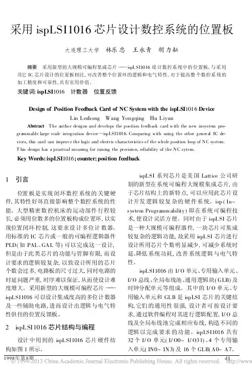
采用ispLSI1016芯片设计数控系统的位置板大连理工大学林乐忠王永青胡力耘摘要采用新型的大规模可编程集成芯片)))ispL SI1016设计数控系统中的位置板,与采用其它IC芯片设计的位置板相比,可改善整个位置环的逻辑和电气特性,对于提高整个数控系统的加工精度和可靠性,具有实用价值。
关键词:ispLSI1016计数器位置反馈Design of Position Feedback C ard of NC System with the ispLSI1016DeviceLin Lezhong Wang Yongqing Hu LiyunAbstract T he autho r desig ns and develops the position feedback card w ith the new insystem pro-gr ammable large scale integ ration device)paring with using the other g ener al IC de-vices,this card can improv e the logic and electr ic character i stics o f the whole position loop of N C system.T his design has a practical meaning for raising the pr ecisio n,reliability of the N C sytem.Key Words:ispLSI1016;counter;position feedback1引言位置板是实现闭环数控系统的关键硬件,其特性好坏直接影响整个数控系统的性能。
大型精密数控机床的运动部件行程较长,必须用位数多的位置板构成位置环,以实现位置闭环控制,这要求设计多位计数器。
用标准的IC芯片或一般的可编程逻辑器件PLD(如PAL、GAL等)可以完成这一设计,但是由于此类芯片的功能与管脚有限,而设计要求的逻辑较复杂,以致设计所用的芯片个数会过多,电路板的尺寸过大,同时电路的时延问题严重,时序难以保证,从而使设计难度增大。
---------------------元器件的分类:semiconductor, electronic components, integrated circuits (IC), passive components, active components, connectors, resistors, capacitors, diodes, transistors, switches, sockets一般分主动和被动元器件。
主动类的主要是指集成电路,就是我们说的IC或芯片;被动类的指接插件、电阻、电容、二极管、三极管、开关、插座等。
我们的业务多集中在主动类(体积小、价值大),兼做被动类(体积大、价值一般小,但也有很贵的)。
-------------------元器件厂家:brand, manufacturer全球有5000家以上行业认可的元器件生产厂家,生产的元器件有百万种之多,而且不断的推陈出新,用新产品来替代老产品。
元器件行业是现代工业的基础。
所有的电子产品都需要元器件来做成成品。
好比是建筑业,建筑公司就是我们现在说的OEM (original equipment manufacturer)。
他们采购不同的建筑材料(对我们就是元器件)来做房子(对我们就是电子产品和设备)。
众多的厂家生产的产品,其实独一无二的很少(哪怕是Intel生产的CPU,其他也有生产的,比如AMD、TI和Cyrix),某一厂家生产的大多数产品都有其他的厂家能生产,只不过在具体的性能指标上有这样那样的不同,很多是可以互相替换的。
缩写:MOT: Motorola 摩托罗拉TI: Texas Instrument 德州仪器NS: National Semiconductor美国国家半导体公司Int: IntelAMD: Advanced Micro DevicesAD: Analog Devices美国模拟器件公司Ray: Raytheon美国雷神公司BB: Burr-BrownHar: Harris哈里斯公司Sie: Siemens西门子LT: Linear Tech 凌力尔特公司Level1: Level OneTosh: Toshiba东芝Sam: Samsung 三星CY: Cypress 美国CYPRESS半导体公司Fuji: Fujitsu日本富士通公司GS: General Semiconductor美国通用仪器公司半导体公司GI: General InstrumentHP: Hewlett-Packard 惠普Hit: Hitachi 日立Lat: Lattice莱迪斯半导体公司TI: Texas Instrument德州PH: PhilipsST: SGS-Thomson Microelectronics汤姆逊电子集团---------------------型号的含义:part#, part number, pin number所有元器件都通过型号来标识。

在系统可编程逻辑器件ispLSi 1016的原理及其在教学实验中的应用李辉【期刊名称】《今日电子》【年(卷),期】1997(000)006【摘要】美国Lattice半导体公司推出的高密度在系统可编程ispLSI(In-System Programmable LargeScale Integration)逻辑器件,除了具备可编程逻辑器件PLD 的优点外,又增加了灵活的在系统可编程功能。
用户可在自己设计的数字系统中或电路板上,对ispLSI逻辑器件进行编程,无需将芯片从电路板上取下来,也不需要加编程高压,即可反复修改,重复定义,现场调试和验证。
ispLSI逻辑器件几乎可以实现所有类型的数字逻辑电路的功能,这使得在一块芯片上由用户自己来实现大规模数字系统的设想成了现实。
克服了专用数字集成电路设计周期长,投入费用高的缺点。
其先进的设计思想和灵活的在系统可编程方式,反映了当代数字系统的一种趋势。
【总页数】3页(P63-65)【作者】李辉【作者单位】中国科技大学电子技术部【正文语种】中文【中图分类】G484【相关文献】1.ispLSI1016器件在数字频率计中的应用 [J], 叶峰;韩德红2.可编程逻辑器件ispLSI1016及其应用 [J], 杨翠娥3.复杂可编程逻辑器件CPLD专题讲座(Ⅰ)──PLSI和ISPLSI的原理及应用 [J], 李景华4.复杂可编程逻辑器件CPLD专题讲座(Ⅲ)──PLSI/ISPLSI2000和3000系列的原理及应用 [J], 李景华5.复杂可程逻辑器件CPLD专题讲座(Ⅱ)──PLSI/ISPLSI 1000系列的原理及应用[J], 李景华因版权原因,仅展示原文概要,查看原文内容请购买。
摘要:介绍了一种基于usb总线的高速数据采集系统,讨论了usb控制器ez-usb控方式实现数据传输的软件设计方法。
关键词:usb;数据采集;ez-usbfx2;gpif1引言现代工业生产和科学研究对数据采集的要求日益提高。
目前比较通用的是在pc或工控机内安装数据采集卡(如a/d卡及422、485卡)。
但这些数据采集设备存在以下缺陷:安装麻烦、价格昂贵、受计算机插槽数量、地址、中断资源的限制,可扩展性差,同时在一些电磁干扰性强的测试现场,可能无法专门对其作电磁屏蔽,从而导致采集的数据失真。
传统的外设与主机的通讯接口一般是基于pci总线、isa总线或者是rs-232c串行总线。
pci总线虽然具有较高的传输速度(132mbps),并支持“即插即用”功能,但其缺点是插拔麻烦,且扩展槽有限(一般为5~6个),isa总线显然存在同样的问题。
rs-232c串行总线虽然连结简单,但其传输速度慢(56kbps),且主机的串口数目也有限。
通用串行总线(universalserialbus,简称usb)是1995年康柏、微软、ibm、dec等公司为了解决传统总线的不足,而推出的一种新型串行通信标准。
该总线接口具有安装方便、高带宽、易扩展等优点,已经逐渐成为现代数据传输的发展趋势。
基于usb的数据采集系统充分利用usb总线的上述优点,有效地解决了传统数据采集系统的缺陷。
usb的规范能针对不同的性能价格比要求提供不同的选择,以满足不同的系统和部件及相应不同的功能,从而给使用带来极大方便。
2系统介绍2.1数据采集系统的结构与功能常见的数据采集系统的硬件总体结构如图1所示。
其中数据采集接口卡是硬件部分的核心,它包括a/d转换器、微控制器、usb通的芯片。
ad8321是美国ad公司生产的一种增益可编程线性驱动器。
它具有频带宽、噪声低、增益可编程且易于与单片机进行串行通信等优点,十分适合在数据采集系统中做前置放大。
经过调理后的信号可送入模/数变换器(adc)进行a/d变换。
FPGA型号命名规则ALTERA产品型号命名XXX XX XX X XX X X1 2 3 4 5 6 7工艺 + 型号 + LE数量 + 封装 + 管脚数目+ 温度范围 + 器件速度。
1.前缀: EP 典型器件EPC 组成的EPROM 器件EPF FLEX 10K 或FLFX 6000 系列、FLFX 8000 系列 EPM MAX5000 系列、MAX7000 系列、MAX9000 系列 EPX 快闪逻辑器件 2.器件型号3. LE数量: XX(k) 4.封装形式:D 陶瓷双列直插Q 塑料四面引线扁平封装 P 塑料双列直插R 功率四面引线扁平封装 S 塑料微型封装T 薄型J 形引线芯片载体 J 陶瓷J 形引线芯片载体 W 陶瓷四面引线扁平封装 L 塑料J 形引线芯片载体 B 球阵列5.管脚6.温度范围:C ℃至70℃,I -40℃至85℃, M -55℃至125℃7.速度:数字越小速度越快。
举例:EP2C20F484C6 EP 工艺2C cyclone2 (S代表stratix。
A代表arria) 20 2wLE数量F484 FBGA484pin 封装 C6 八速LE数量在同等器件信号的同时越多的越好,同时越贵。
管脚数量在同等情况下越多越好。
器件速度越快越好。
FPGA可能没有先进性一说:不同产品不同用途。
cyclone系列:一共3代(目前已有5代)cyclone系列是FPGA的A版入门产品。
涵盖面广,而且对应的器件无论功耗和速度都不错。
在小规模设计上与xilinx的spartan3A竞争低端市场。
stratix:总共4代的stratix直瞄大规模。
数字信号处理以及片上系统等高端市场。
无论是器件速度还是内部资源都是全新的构架。
至于片上系统以及内部DSP,stratix4和高端xilinx vertix5成为了两大公司在高端市场的主流。
xilinx公司fpga芯片命名规则例如XC3S2000-5FGG676CXC3S是SPARTAN系列器件类型2000是200万个系统门-5是高性能FGG676是676引脚FBGA封装C是商用常用CPLD/FPGA 标识的含义CPLD/FPGA生产厂家多,系列、品种更多,各生产厂家命名、分类不一,给CPLD/FPGA 的应用带来了一定的困难,但其标识也是有一定的规律的。
Lattice 产品一、公司简介Lattice半导体公司(Lattice Semiconductor)成立于1983年,专业从事设计、开发和销售高性能的可编程逻辑器件和相关软件。
Lattice是ISP(In System Programmable)技术的发明者,ISP技术极大的促进了PLD产品的发展。
1999年收购V antis(原AMD子公司),2001年收购Lucent微电子的FPGA部门,是世界第三大可编程逻辑器件供应商。
目前Lattice公司在上海设有研发部门。
二、Lattice的ISP技术Lattice公司于1991 年革命性地率先推出高密度在系统可编程(In System Programmable)逻辑器件,从而开创了可编程逻辑器件的市场。
通过使用ISP器件,工程师们可以在电路板上直接对可编程器件进行编程或再编程,有效缩短产品上市周期、降低生产成本。
Lattice开发的ISP 技术使用户在产品的整个寿命周期中获得无形的利益。
从设计、制造到现场升级、维护,采用Lattice ISP 产品可以加速产品的上市并降低研发成本。
Lattice ISP 技术帮助工程师缩短系统试制时间、简化生产流程并采用经证实更有效的方式进行现场升级和维护。
三、Lattice的产品线Lattice目前主要有6个产品系列:●CPLDComplex Programmable Logic Device●ispXPLDeXpanded Programmable Logic Devices●ispXPGA●ORCA FPSC●IspPAC●ispGDX2Lattice 的所有产品都具备isp功能,即所有芯片均可满足在线配置或重配置。
四、CPLD——Complex Programmable Logic Device1、CPLD的性能Lattice的CPLD颇有特色,在业界具有很强的竞争力,包括早期的ispLSI系列产品和MACH系列、ispMACH4000系列、ispLSI5000系列、和ispMACH5000系列产品。