LM2-100J-TR中文资料
- 格式:pdf
- 大小:16.30 KB
- 文档页数:1
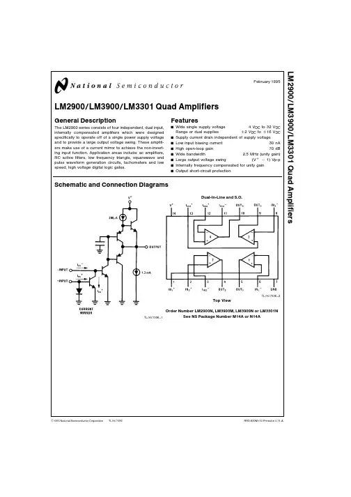
TL H 7936LM2900 LM3900 LM3301Quad AmplifiersFebruary 1995LM2900 LM3900 LM3301Quad AmplifiersGeneral DescriptionThe LM2900series consists of four independent dual input internally compensated amplifiers which were designed specifically to operate off of a single power supply voltage and to provide a large output voltage swing These amplifi-ers make use of a current mirror to achieve the non-invert-ing input function Application areas include ac amplifiers RC active filters low frequency triangle squarewave and pulse waveform generation circuits tachometers and low speed high voltage digital logic gatesFeaturesY Wide single supply voltage 4V DC to 32V DCRange or dual suppliesg 2V DC to g 16V DC Y Supply current drain independent of supply voltage Y Low input biasing current 30nA Y High open-loop gain 70dB Y Wide bandwidth 2 5MHz (unity gain)Y Large output voltage swing (V ab 1)Vp-p Y Internally frequency compensated for unity gain YOutput short-circuit protectionSchematic and Connection DiagramsTL H 7936–1Dual-In-Line and S OTL H 7936–2Top ViewOrder Number LM2900N LM3900M LM3900N or LM3301NSee NS Package Number M14A or N14AC 1995National Semiconductor Corporation RRD-B30M115 Printed in U S AAbsolute Maximum RatingsIf Military Aerospace specified devices are required please contact the National Semiconductor Sales Office Distributors for availability and specificationsLM2900 LM3900LM3301 Supply Voltage32V DC28V DCg16V DC g14V DC Power Dissipation(T A e25 C)(Note1)Molded DIP1080mW1080mWS O Package765mWInput Currents I IN a or I IN b20mA DC20mA DC Output Short-Circuit Duration One Amplifier Continuous ContinuousT A e25 C(See Application Hints)Operating Temperature Range b40 C to a85 C LM2900b40 C to a85 CLM39000 C to a70 CStorage Temperature Range b65 C to a150 C b65 C to a150 C Lead Temperature(Soldering 10sec )260 C260 C Soldering InformationDual-In-Line PackageSoldering(10sec )260 C260 C Small Outline PackageVapor Phase(60sec )215 C215 C Infrared(15sec )220 C220 CSee AN-450‘‘Surface Mounting Methods and Their Effect on Product Reliability’’for other methods of soldering surface mount devicesESD tolerance(Note7)2000V2000V Electrical Characteristics T A e25 C V a e15V DC unless otherwise statedParameter ConditionsLM2900LM3900LM3301Units Min Typ Max Min Typ Max Min Typ MaxOpen Voltage Gain Over TempV mV Loop Voltage Gain D V O e10V DC1 22 81 22 81 22 8Input Resistance Inverting Input111M XOutput Resistance889k XUnity Gain Bandwidth Inverting Input2 52 52 5MHzInput Bias Current Inverting Input V a e5V DC302003020030300nAInverting InputSlew Rate Positive Output Swing0 50 50 5V m s Negative Output Swing202020Supply Current R L e%On All Amplifiers6 2106 2106 210mA DCOutput V OUT High R L e2k I IN b e013 513 513 5Voltage V a e15 0V DC I IN a e0Swing VOUT Low I IN b e10m A0 090 20 090 20 090 2I IN a e0V DCV OUT High V a e Absolute I IN b e0Maximum Ratings I IN a e029 529 526 0R L e%Output Source618610518Current Sink(Note2)0 51 30 51 30 51 3mADC CapabilityI SINK V OL e1V I IN b e5m A5552Electrical Characteristics(Note6) V a e15V DC unless otherwise stated(Continued)Parameter ConditionsLM2900LM3900LM3301Units Min Typ Max Min Typ Max Min Typ MaxPower Supply Rejection T A e25 C f e100Hz707070dB Mirror Gain 20m A(Note3)0 901 01 10 901 01 10 9011 10m A m A 200m A(Note3)0 901 01 10 901 01 10 9011 10D Mirror Gain 20m A to200m A(Note3)252525% Mirror Current(Note4)105001050010500m A DC Negative Input Current T A e25 C(Note5)1 01 01 0mA DC Input Bias Current Inverting Input300300nA Note1 For operating at high temperatures the device must be derated based on a125 C maximum junction temperature and a thermal resistance of92 C W which applies for the device soldered in a printed circuit board operating in a still air ambient Thermal resistance for the S O package is131 C WNote2 The output current sink capability can be increased for large signal conditions by overdriving the inverting input This is shown in the section on Typical CharacteristicsNote3 This spec indicates the current gain of the current mirror which is used as the non-inverting inputNote4 Input V BE match between the non-inverting and the inverting inputs occurs for a mirror current(non-inverting input current)of approximately10m A This is therefore a typical design center for many of the application circuitsNote5 Clamp transistors are included on the IC to prevent the input voltages from swinging below ground more than approximately b0 3V DC The negative input currents which may result from large signal overdrive with capacitance input coupling need to be externally limited to values of approximately1mA Negative input currents in excess of4mA will cause the output voltage to drop to a low voltage This maximum current applies to any one of the input terminals If more than one of the input terminals are simultaneously driven negative smaller maximum currents are allowed Common-mode current biasing can be used to prevent negative input voltages see for example the‘‘Differentiator Circuit’’in the applications sectionNote6 These specs apply for b40 C s T A s a85 C unless otherwise statedNote7 Human body model 1 5k X in series with100pFApplication HintsWhen driving either input from a low-impedance source alimiting resistor should be placed in series with the inputlead to limit the peak input current Currents as large as20mA will not damage the device but the current mirror onthe non-inverting input will saturate and cause a loss of mir-ror gain at mA current levels especially at high operatingtemperaturesPrecautions should be taken to insure that the power supplyfor the integrated circuit never becomes reversed in polarityor that the unit is not inadvertently installed backwards in atest socket as an unlimited current surge through the result-ing forward diode within the IC could cause fusing of theinternal conductors and result in a destroyed unitOutput short circuits either to ground or to the positive pow-er supply should be of short time duration Units can bedestroyed not as a result of the short circuit current causingmetal fusing but rather due to the large increase in IC chipdissipation which will cause eventual failure due to exces-sive junction temperatures For example when operatingfrom a well-regulated a5V DC power supply at T A e25 C with a100k X shunt-feedback resistor(from the output tothe inverting input)a short directly to the power supply willnot cause catastrophic failure but the current magnitude willbe approximately50mA and the junction temperature willbe above T J max Larger feedback resistors will reduce thecurrent 11M X provides approximately30mA an open cir-cuit provides1 3mA and a direct connection from the out-put to the non-inverting input will result in catastrophic fail-ure when the output is shorted to V a as this then places thebase-emitter junction of the input transistor directly acrossthe power supply Short-circuits to ground will have magni-tudes of approximately30mA and will not cause cata-strophic failure at T A e25 CUnintentional signal coupling from the output to the non-in-verting input can cause oscillations This is likely only in breadboard hook-ups with long component leads and can be prevented by a more careful lead dress or by locating the non-inverting input biasing resistor close to the IC A quick check of this condition is to bypass the non-inverting input to ground with a capacitor High impedance biasing resis-tors used in the non-inverting input circuit make this input lead highly susceptible to unintentional AC signal pickupOperation of this amplifier can be best understood by notic-ing that input currents are differenced at the inverting-input terminal and this difference current then flows through the external feedback resistor to produce the output voltage Common-mode current biasing is generally useful to allow operating with signal levels near ground or even negative as this maintains the inputs biased at a V BE Internal clamp transistors(see note5)catch-negative input voltages at ap-proximately b0 3V DC but the magnitude of current flow has to be limited by the external input network For operation at high temperature this limit should be approximately100m A This new‘‘Norton’’current-differencing amplifier can be used in most of the applications of a standard IC op amp Performance as a DC amplifier using only a single supply is not as precise as a standard IC op amp operating with split supplies but is adequate in many less critical applications New functions are made possible with this amplifier which are useful in single power supply systems For example biasing can be designed separately from the AC gain as was shown in the‘‘inverting amplifier ’’the‘‘difference integra-tor’’allows controlling the charging and the discharging of the integrating capacitor with positive voltages and the‘‘fre-quency doubling tachometer’’provides a simple circuit which reduces the ripple voltage on a tachometer output DC voltage3Typical Performance CharacteristicsOpen Loop Gain Voltage Gain Voltage GainLarge Signal Frequency Input Current Supply Current ResponseOutput Sink Current Output Class-A Bias Current Output Source CurrentSupply Rejection Mirror Gain Maximum Mirror CurrentTL H 7936–94Typical Applications(V a e15V DC)Inverting AmplifierV ODC e V a 2A V j b R2R1TL H 7936–3Triangle Square GeneratorTL H 7936–4Frequency-Doubling TachometerTL H 7936–5Low V IN b V OUT Voltage RegulatorTL H 7936–6 Non-Inverting AmplifierV ODC e V a 2A V j R2R1TL H 7936–7Negative Supply BiasingV ODC eR2R3V bTL H 7936–8A V jR2R15Typical Applications (V a e 15V DC )(Continued)Low-Drift Ramp and Hold CircuitTL H 7936–10Bi-Quad Active Filter(2nd Degree State-Variable Network)TL H 7936–11Q e 50f O e 1kHz6Typical Applications(V a e15V DC)(Continued)Voltage-Controlled Current Source(Transconductance Amplifier)TL H 7936–12Hi V IN Lo(V IN b V O)Self-RegulatorQ1 Q2absorb Hi V INTL H 7936–13Ground-Referencing a Differential Input SignalTL H 7936–147Typical Applications(V a e15V DC)(Continued)Voltage Regulator(V O e V Z a V BE)TL H 7936–15Fixed Current SourcesI2e R1R2I1TL H 7936–16Voltage-Controlled Current Sink(Transconductance Amplifier)TL H 7936–17Buffer AmplifierV IN t V BETL H 7936–18TachometerTL H 7936–19V ODC e A f INAllows V O to go to zero8Typical Applications (V a e 15V DC )(Continued)Low-Voltage ComparatorNo negative voltage limit if properly biasedTL H 7936–20Power ComparatorTL H 7936–21Comparator TL H 7936–22Schmitt-TriggerTL H 7936–23Square-Wave Oscillator TL H 7936–24Pulse GeneratorTL H 7936–25Frequency Differencing TachometerV ODC e A (f 1b f 2)TL H 7936–269Typical Applications(V a e15V DC)(Continued)Frequency Averaging TachometerV ODC e A(f1a f2)TL H 7936–27Squaring Amplifier(W Hysteresis)TL H 7936–28Bi-Stable MultivibratorTL H 7936–29Differentiator(Common-Mode Biasing Keeps Input at a V BE)A V e 1 2TL H 7936–30‘‘OR’’Gatef e A a B a CTL H 7936–31‘‘AND’’Gatef e A B CTL H 7936–32Difference IntegratorTL H 7936–33 10Typical Applications (V a e 15V DC )(Continued)Low Pass Active Filterf O e 1kHzTL H 7936–34Staircase GeneratorTL H 7936–35V BE BiasingA V j bR2R1TL H 7936–36Bandpass Active FilterTL H 7936–37f o e 1kHz Q e 2511Typical Applications(V a e15V DC)(Continued)Low-Frequency MixerTL H 7936–38Free-Running Staircase Generator Pulse CounterTL H 7936–3912Typical Applications(V a e15V DC)(Continued)Supplying I IN with Aux Amp(to Allow Hi-Z Feedback Networks)TL H 7936–40One-Shot MultivibratorPW j2c106CSpeeds recoveryTL H 7936–41Non-Inverting DC Gain to(0 0)TL H 7936–4213Typical Applications(V a e15V DC)(Continued)Channel Selection by DC Control(or Audio Mixer)TL H 7936–4314Typical Applications (V a e 15V DC )(Continued)Power AmplifierTL H 7936–44One-Shot with DC Input ComparatorTL H 7936–45Trips at V IN j 0 8VaV IN must fall 0 8Vaprior to t 2High Pass Active FilterTL H 7936–4615Typical Applications(V a e15V DC)(Continued)Sample-Hold and Compare with New a V INTL H 7936–47Sawtooth GeneratorTL H 7936–4816Typical Applications(V a e15V DC)(Continued)Phase-Locked LoopTL H 7936–49Boosting to300mA LoadsTL H 7936–5017Split-Supply Applications(V a e a15V DC V b e b15V DC)Non-Inverting DC GainTL H 7936–51AC AmplifierTL H 7936–5218Physical Dimensions inches(millimeters)Small Outline Package(M)Order Number LM3900MNS Package Number M14A19L M 2900 L M 3900 L M 3301Q u a d A m p l i f i e r sPhysical Dimensions inches (millimeters)(Continued)Molded Dual-In-Line Package (N)Order Number LM2900N LM3900N or LM3301NNS Package Number N14ALIFE SUPPORT POLICYNATIONAL’S PRODUCTS ARE NOT AUTHORIZED FOR USE AS CRITICAL COMPONENTS IN LIFE SUPPORT DEVICES OR SYSTEMS WITHOUT THE EXPRESS WRITTEN APPROVAL OF THE PRESIDENT OF NATIONAL SEMICONDUCTOR CORPORATION As used herein 1 Life support devices or systems are devices or 2 A critical component is any component of a life systems which (a)are intended for surgical implant support device or system whose failure to perform can into the body or (b)support or sustain life and whose be reasonably expected to cause the failure of the life failure to perform when properly used in accordance support device or system or to affect its safety or with instructions for use provided in the labeling can effectivenessbe reasonably expected to result in a significant injury to the userNational Semiconductor National Semiconductor National Semiconductor National Semiconductor CorporationEuropeHong Kong LtdJapan Ltd1111West Bardin RoadFax (a 49)0-180-530858613th Floor Straight Block Tel 81-043-299-2309。
LM2-100*3000铝门窗双头组角机使用说明书济南西格玛机器有限公司地址:济南天桥工业开发区兴业路8号邮编:250023销售热线:(0531)85709308传真:(0531)85765600网址:邮箱:jn.xgm2006@目次1.主要用途与适用范围2.主要技术参数3.主要结构、工作原理及特点4.安装与调整5.操作流程6.维护与保养7.常见故障及排除方法8.附图图1 刀具调整示意图图2 机构组成示意图图3 外形简图图4 气、液压系统原理图图5 电气原理图1 主要用途与适用范围LM2-100*3000型铝门窗双头组角机是加工高档铝门窗的专用设备。
可一次完成两个角的角码式冲铆连接。
2 主要技术参数输入电压:380V 50Hz(三相四线)输入功率:4Kw工作气压:0.5~0.8MPa耗气量:约200L/次额定油压:15MPa油箱容量:60L两机头最大开距:max3000mm组角缸运动行程:50mm组装最小框尺寸:450 mm适应型材的宽度/高度:50~100 mm/40~100 mm重量:600kg3 主要结构、工作原理及特点3.1 主要结构本机主要由床身、固定机头、活动机头、内定位装置、外定位装置、压紧机构、液压系统、电控系统、气动系统、托料架等部分组成。
见外形简图。
工作原理内、外定位装置、压紧机构及型材预紧装置限定三根型材的位置,先由低压油供给组角缸调试,使组角刀调整到待冲铆动作,再由高压油实现冲铆动作,完成组角。
3.3 特点该机压紧机构自动伸缩,内、外定位块上下可调,并可叠加使用,组角缸前后、左右可调,可用于各种规格、截面的型材,适应性强;运动部分采用高精度直线运动副,组角精度高;液压组角缸可提供足够的冲铆力,角连接强度大;一次可组接两个90°角,工作效率高。
4 安装与调整4.1 环境与要求组角机应安装在干燥,无粉尘,无腐蚀性气体的室内坚硬水泥地面上。
4.2 开箱到位开箱后将组角机连同移至安装位置旁,拆下包装底座,使用搬动工具将组角机移至安装位置。