SMB 600W Series
- 格式:pdf
- 大小:698.23 KB
- 文档页数:4

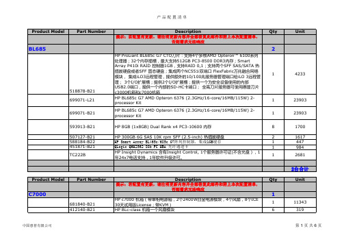
u可扩展的网络存储解决方案:控制器单元拥有60个内部硬盘,可通过先进SAS 接口连接的扩展单元扩展u可配置基于硬件的RAID/DDP 保护(RAID‑5、RAID‑6或DDP )以达到最高系统性能u 冗余的热插拔电源设备和冷却风扇u 两个用于高速iSCSI 连接的万兆位以太网端口u模块化设计,方便维修,享受NetApp 服务,包括3年下一工作日现场支持DSA E2800代表下一代DSA E‑Series ,即博世推出的基于iSCSI 的数字视频磁盘阵列。
专为安防领域设计的专业平台,可满足该领域苛刻的数字视频存储应用要求,能够管理不断增多的数字视频数据。
随着高清以及最近的超高清(4K)IP 摄像机和编码器进入监控市场,该应用面临的主要挑战在于存储基础架构的高带宽和低复杂度方面不断增长的需求。
下一代DSA E2800磁盘阵列可解决这一难题。
系统概述DSA E2800基于4U 双控制器单元,内部拥有60个3.5英寸7.2K 转速的NL-SAS (串行连接SCSI )企业级硬盘(近线SAS ),可满足大容量和高性能的要求。
该存储系统是具有超强灵活性设计的高性能解决方案,非常适合广泛的视频监控要求。
其平衡性能设计用于支持高带宽和I/O 密集型工作负载。
DSA E2800磁盘架选件有一个高密度60盘位扩展单元,可配备60个3.5英寸7.2K 转速的NL-SAS 企业级硬盘(4U),可实现自定义配置以针对各种标准的中大型企业环境进行优化。
再者,DSA E2800的完全冗余I/O 路径、高级保护功能和广泛诊断能力带来高水准的可用性、完整性和安全性。
功能DSA E2800是NetApp 公司推出的联合品牌E2800系列。
它是一种向上扩展的网络存储解决方案,为您的所有视频数据提供优异的安全性、高度“现成”的扩展性、值得信赖的数据保护以及简化的管理。
NetApp 多年前率先采用iSCSI 协议,并为视频监控市场打造出新一代E2800系列高端产品。

产品概况Spirent Communications 公司的SmartBits 600B(SMB-600B)是业界中便携性能最强,最小巧的一种相对高端口密度的性能分析系统。
该系统与SMB-6000B 完全兼容,SMB-600B 最多支持两个模块,以及最多16 个10/100 Mbps以太网端口,4 个SmartMetrics™ 千兆以太网端口,4 个光纤通道端口,1 个10GbE 端口,或以上各种端口的组合。
如配置一块LAN-3101B(包含6个10/100M接口)和一块LAN-3320A(包含2个双介质10/100/1000M接口),或2块LAN-3101B板卡或2块LAN-3320A板卡。
SMB-600 可以串连在一起使用,从而获得更高的端口密度,使用户能够在质量控制和大容量生产环境中执行自动化的大规模测试。
通过使用SmartBits 多机扩展单元,还可将最多512 台机器同步连接起来。
用户可以通过一台PC 上的10/100 Mbps 以太网接口和基于Windows®的用户界面,非常轻松地对对SMB-600B 实施有效的控制。
SMB-600B 的设计用途包括:网络设备制造商:测试您的设备,然后还可以将网络设备和SMB-600B 携带到客户的地点,并现场展示您设备的性能。
评测实验室:测试和认证来自多个制造商的不同设备,并对其性能进行评测。
电信公司、ISP 和企业用户:对网络设备进行比较分析,在设备部署之前判定其的适用性。
SMB-600B 的特性◆小巧、轻便,可携带。
◆最多可容纳2 张模块。
◆最多支持16 个10/100 Mbps 以太网端口,4 个SmartMetrics™ 千兆以太网端口,4 个光纤通道端口,1 个10GbE 端口,或以上各型端口的组合。
◆捆绑了三个基于PC 的应用软件,可以提供全面的性能分析功能(SmartWindow™ 、SmartLib™ 和SmartApplications™ )。

MECHANICAL DATACase: SMB (DO-214AA)Molding compound meets UL 94 V-0 flammability rating Base P/N-E3 - RoHS-compliant, commercial gradeBase P/N-M3 - halogen-free, RoHS-compliant, commercial gradeBase P/NHE3_X - RoHS-compliant and AEC-Q101 qualified Base P/NHM3_X - halogen-free, RoHS-compliant, and AEC-Q101 qualified(“_X” denotes revision code e.g. A, B, ..... and only available for 250 V to 540 V type)Terminals: matte tin plated leads, solderable per J-STD-002 and JESD 22-B102E3, M3, HE3, and HM3 suffix meets JESD 201 class 2 whisker testPolarity: for uni-directional types the band denotes cathode end, no marking on bi-directional typesNotes(1) Non-repetitive current pulse, per fig. 3 and derated above T A= 25 °C per fig. 2 (2) Mounted on 0.2" x 0.2" (5.0 mm x 5.0 mm) copper pads to each terminalFEATURES• Low profile package• Ideal for automated placement • Glass passivated chip junction• Available in uni-directional and bi-directional • 600 W peak pulse power capability with a 10/1000 μs waveform, repetitive rate (duty cycle): 0.01 %• Excellent clamping capability • Very fast response time• Low incremental surge resistance• Meets MSL level 1, per J-STD-020, LF maximum peak of 260 °C• AEC-Q101 qualified available- Automotive ordering code: base P/NHE3 or P/NHM3(1) Pulse test: t p 50 ms(2) Surge current waveform per fig. 3 and derate per fig. 2(3) For bi-directional types with V WM of 10 V and less, the I D limit is doubled(4) All terms and symbols are consistent with ANSI/IEEE CA62.35(5) V F = 3.5 V at I F = 50 A (uni-directional only)RATINGS AND CHARACTERISTICS CURVES (T A = 25 °C unless otherwise noted)1001011007550250.10.1 µs 1.0 µs 10 µs 100 µs 1.0 ms 10 ms0 25 50 75 100125 150 175 200t d - Pulse Width (s) TJ - Initial Temperature (°C) Fig. 1 - Peak Pulse Power Rating Curve Fig. 2 - Pulse Power or Current vs. Initial Junction TemperatureFig. 3 - Pulse Waveform Fig. 5 - Typical Transient Thermal Impedance Fig. 4 - Typical Junction Capacitance Fig. 6 - Maximum Non-Repetitive Peak Forward Surge Current PPPM-PeakPulsePower(kW)PeakPulsePower(PPP)orCurrent(IPP)DeratinginPercentage,%。
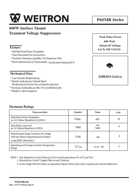
WEITRON600W Surface MountPeak Pulse Power 600 Watt Stand-off Voltage 6.8 To 550 VOLTSTransient Voltage Suppressors* 600 Watt Peak Power Dissipation * Glass Passivated Die Construction* Excellent Clamping Capability Fast Response Time* Plastic Material Has UL Flammability Classification Rating 94V-O* Case: Transfer Molded Epoxy* Polarity: Indicator by Cathode Band* Terminals: Solderable per MIL-STD-202 Method 208* Weight: 0.1grams(approx)(Bi-directional Devices Has no Polarity Indicator)NOTE: 1. Non-Repetitive Current Pulse, per FIG3 and Derated 2. Mounted on 5.0mm Copper Pads to each Terminal3. 8.3ms Single Half Sine-Wave, or equivalent Square above TA=25 C per FIG2Wave, Duty Cycle=4 pulses per minutes Maximum.Maximum Ratings2UNI- POLAR BI-POLAR(1)UNI BI P6SMB6.8A P6SMB7.5A P6SMB8.2A P6SMB9.1A P6SMB10A P6SMB11A P6SMB12A P6SMB13A P6SMB15A P6SMB16A P6SMB18A P6SMB20A P6SMB22A P6SMB24A P6SMB27AP6SMB30A P6SMB33A P6SMB36A P6SMB39A P6SMB43A P6SMB47A P6SMB51A P6SMB56A P6SMB62A P6SMB68A P6SMB75A P6SMB82A P6SMB91A P6SMB100A P6SMB110A P6SMB120A P6SMB130A P6SMB150A P6SMB160A P6SMB170A P6SMB180A P6SMB200A P6SMB220A P6SMB250A P6SMB300A P6SMB350A P6SMB400A P6SMB440A P6SMB480A P6SMB510A P6SMB530A P6SMB540A P6SMB550A P6SMB6.8CA P6SMB7.5CA P6SMB8.2CA P6SMB9.1CA P6SMB10CA P6SMB11CA P6SMB12CA P6SMB13CA P6SMB15CA P6SMB16CA P6SMB18CA P6SMB20CA P6SMB22CA P6SMB24CA P6SMB27CA P6SMB30CA P6SMB33CA P6SMB36CA P6SMB39CA P6SMB43CA P6SMB47CA P6SMB51CA P6SMB56CA P6SMB62CA P6SMB68CA P6SMB75CA P6SMB82CA P6SMB91CA P6SMB100CA P6SMB110CA P6SMB120CA P6SMB130CA P6SMB150CA P6SMB160CA P6SMB170CA P6SMB180CA P6SMB200CA P6SMB220CA P6SMB250CA P6SMB300CA P6SMB350CA P6SMB400CA P6SMB440CA P6SMB480CA P6SMB510CA P6SMB530CA P6SMB540CA P6SMB550CA 6V8A 5.80 6.451010.558.110007V5A 6.407.131011.354.08008V2A 7.027.791012.150.42009V1A 7.788.651013.445.55010A 8.559.50114.542.11011A 9.4010.50115.639.1512A 10.2011.40116.736.5513A 11.1012.40118.233.5515A 12.8014.30121.228.8516A 13.6015.20122.527.1518A 15.3017.10125.524.2520A 17.1019.00127.722.0522A 18.8020.90130.619.9524A 20.5022.80133.218.4527A 23.1025.70137.516.3530A 25.6028.50141.414.7533A 28.2031.40145.713.3536A 30.8034.20149.912.2539A 33.3037.10153.911.3543A 36.8040.90159.310.3547A 40.2044.70164.89.4551A 43.6048.50170.18.7556A 47.8053.20177.07.9562A 53.0058.90185.07.2568A 58.1064.60192.0 6.6575A 64.1071.301103.0 5.9582A 70.1077.901113.0 5.4591A 77.8086.501125.0 4.95100A 85.5095.001137.0 4.55110A 94.00105.001152.0 4.05120A 102.00114.001165.0 3.75130A 111.00124.001179.0 3.45150A 128.00143.001207.0 2.95160A 136.00152.001219.0 2.85170A 145.00162.001234.0 2.65180A 154.00171.001246.0 2.55200A 171.00190.001274.0 2.25220A 185.00209.001328.0 1.95250A 214.00237.001344.0 1.85300A 256.00285.001414.0 1.55350A 300.00332.001482.0 1.35400A 342.00380.001548.0 1.15440A 376.00418.001602.0 1.05480A 408.00456.001658.00.95510A 434.00485.001698.00.95530A 540A 550A 6V8C 7V5C 8V2C 9V1C 10C11C12C13C 15C16C18C20C 22C24C 27C 30C 33C36C 39C 43C 47C51C56C62C 68C75C82C91C100C 110C 120C 130C 150C 160C 170C 180C 200C 220C 250C 300C 350C 400C 440C 480C 510C 530C 540C 550C 450.00459.00467.00503.50513.00522.507.147.888.619.5510.5011.6012.5013.7015.8016.8018.9021.0023.1025.2028.4031.5034.7037.8041.0045.2049.4053.6058.8065.1071.4078.8086.1095.50105.00116.00126.00137.00158.00168.00179.00189.00210.00231.00263.00315.00368.00420.00462.00504.00535.00556.50567.00577.50111725.0740.0760.00.80.80.8555For bidirectional type having Vrwm of 10 volts and less, the IR limit is double.for parts without A , the V BR is + + 10%.BREAK DO WN VOLTAGE V BR (V)(1)V BR (V)(2)MAX.@I TTEST CURRE NT I T (mA)MAXIMUM CLAMPING VOLTAGE @Ipp Vc(V)PEAK PULSE CURRENT Ipp (A)P6SMBPART NUMBER DEVICE MARKING CODEREVERSE STAND-OFF VOLTAGE V RWM (V)MIN.@I T REVERSE LEAKAGE @ V RWMI R (µA)(3)Electrical characteristicsNOTE: 1. Suffix C denotes Bi-direction device, Suffix A denotes the V is 5% BR2. V messured with I Current pulse=300us.BRT 3.WEITRONWEITRONP P P M — P e a k P u l s e P o w e r (k W )FIG. 6 - Maximum Non-Repetitive PeakForward Surge CurrentNumber of C ycles at 60H Z11100t p — P ulse Duration (sec)T r a n s i e n t T h e r m a l I m p e d a n c e (C /W )FIG. 5 - Typical T ransient ThermalImpedance0.0010.010.11101001000I P P M — P e a k P u l s e C u r r e n t , % I R S MRatings and Characteristic CurvesSMB Outline DimensionWEITRON。
samba服务器配置说明配置服务器密码:cnfoldcsamba相关命令grep -v '^#' smb.conf |grep -v '^;' |grep -v '^$' 确认是否把设定给批注了/etc/rc.d/init.d/smb restart 重启smb服务vi /etc/samba/smb.conf 修改samba配置文件smb.confifconfig eth0 169.254.235.182 netmask 255.255.0.0 up 临时修改IP地址和网关samba设定档:/etc/samba/smb.conf这个是samba最主要的设定档/etc/samba/lmhosts这个档案主要目的在对应NetBIOS name 与该主机名称的IP/etc/samba/smbpasswd 档案预设不存在是samba预设使用者密码对应表需要权限root且设定为600samba相关目录:/usr/share/doc/samba 这个目录包含了samba的所有相关技术手册/var/log/samba这个目录是samba预设的登录文件放置目录可以查看是否被入侵/usr/share/samba/codepages这个目录是放置各个语言的支持格式需要支持中文就靠codepage.950支持。
当然修改smb.conf是最直接的。
[global]workgroup : 工作群组:同一个局域网络内,要具有相同的workgroupnetbios name : 主机名称:这个主机名称就是netbios 的名字!请注意,如果你没有设定netbios 的话,预设的netbios 会以hostname 来替代!server string: 这个是主机的说明,随便写写没关系!security : 这个重要,是用来规定samba 主机的安全登入项目,有底下几种:share :不进行安全登入,亦即没有设定账号与密码user:设定主机的密码文件作为登入的验证档案,这与底下的smb passwd file有关domain :就是让您的samba 作为PDC 啰!log file : 登录文件放置的目录所在地[webpage]comment = my home page 这个是目录说明path =/var/www/htmlread only =no 是否只读public = yes 是否让所有可以登入的使用者看到这个项目writable =yes 是否可以写入读写权限值最后出现的那个设置值为主这里起作用的是 writable而不是read onlycreate mode =0664directory mode =0775 这两个mode都与权限有关samba变量%s :取代目前的设定项目值,所谓的『设定项目值』就是在里面的内容!举例来说:[homes]valid users=%s因为 validusers是允许的登入者,设定为%s 表示任何可登入的使用者都能够登入的意思~今天如果test 这个使用者登入之后,那个[homes] 就会自动的变成了[test]了!这样可以明白了吗?!%s 的用意就是在替换掉目前[] 里面的内容啦!%m :代表 client端的NetBIOS 主机名称喔!例如上面案例的登录档!%M :代表 client端的Internet 主机名称喔!就是HOSTNAME 。
P6SMB91AT3G P6SMB75AT3G P6SMB13AT3G P6SMB200AT3G.P6SMB160AT3G P6SMB27AT3G.P6SMB33AT3G.P6SMB51AT3G P6SMB16AT3GP6SMB6.8AT3 Series600 Watt Peak Power Zener Transient Voltage SuppressorsUnidirectional*The SMB series is designed to protect voltage sensitivecomponents from high voltage, high energy transients. They have excellent clamping capability, high surge capability, low zener impedance and fast response time. The SMB series is supplied in ON Semiconductor’s exclusive, cost-effective, highly reliable Surmetic™ package and is ideally suited for use in communication systems, automotive, numerical controls, process controls, medical equipment, business machines, power supplies and many other industrial/consumer applications.Specification Features:•Working Peak Reverse V oltage Range − 5.8 to 171 V •Standard Zener Breakdown V oltage Range − 6.8 to 200 V •Peak Power − 600 W @ 1 ms•ESD Rating of Class 3 (>16 KV) per Human Body Model •Maximum Clamp V oltage @ Peak Pulse Current•Low Leakage < 5 m A Above 10 V•UL 497B for Isolated Loop Circuit Protection •Response Time is Typically < 1 ns•Pb−Free Packages are AvailableMechanical Characteristics:CASE:V oid-free, transfer-molded, thermosetting plasticFINISH:All external surfaces are corrosion resistant and leads are readily solderableMAXIMUM CASE TEMPERATURE FOR SOLDERING PURPOSES: 260°C for 10 SecondsLEADS:Modified L−Bend providing more contact area to bond pads POLARITY:Cathode indicated by polarity bandMOUNTING POSITION:AnyMAXIMUM RATINGSPlease See the Table on the Following Page*Please see P6SMB11CAT3 to P6SMB91CAT3 for Bidirectional devices.Device Package Shipping†ORDERING INFORMATIONP6SMBxxxAT3SMB2500/Tape & ReelSMBCASE 403APLASTICP6SMBxxxAT3G SMB(Pb−Free)2500/Tape & Reel†For information on tape and reel specifications, including part orientation and tape sizes, please refer to our T ape and Reel Packaging Specifications Brochure, BRD8011/D.A= Assembly LocationY= YearWW= Work Weekxx= Device Code (Refer to page 3)G= Pb−Free PackageMARKING DIAGRAMAYWWxx GG(Note: Microdot may be in either location)MAXIMUM RATINGSRating Symbol Value Unit Peak Power Dissipation (Note 1) @ T L = 25°C, Pulse Width = 1 ms P PK600WDC Power Dissipation @ T L = 75°C Measured Zero Lead Length (Note 2) Derate Above 75°CThermal Resistance from Junction−to−LeadP DR q JL3.04025WmW/°C°C/WDC Power Dissipation (Note 3) @ T A = 25°C Derate Above 25°CThermal Resistance from Junction−to−AmbientP DR q JA0.554.4226WmW/°C°C/WForward Surge Current (Note 4) @ T A = 25°C I FSM100A Operating and Storage Temperature Range T J, T stg−65 to +150°C Stresses exceeding Maximum Ratings may damage the device. Maximum Ratings are stress ratings only. Functional operation above the Recommended Operating Conditions is not implied. Extended exposure to stresses above the Recommended Operating Conditions may affect device reliability.1.10 X 1000 m s, non−repetitive2.1″ square copper pad, FR−4 board3.FR−4 board, using ON Semiconductor minimum recommended footprint, as shown in 403A case outline dimensions spec.4.1/2 sine wave (or equivalent square wave), PW = 8.3 ms, duty cycle = 4 pulses per minute maximum.ELECTRICAL CHARACTERISTICS(T A = 25°C unless otherwise noted, V F = 3.5 V Max. @I F (Note 4) = 30 A) (Note 5)Symbol ParameterI PP Maximum Reverse Peak Pulse CurrentV C Clamping Voltage @ I PPV RWM Working Peak Reverse VoltageI R Maximum Reverse Leakage Current @ V RWMV BR Breakdown Voltage @ I TI T Test CurrentQ V BR Maximum Temperature Coefficient of V BRI F Forward CurrentV F Forward Voltage @ I F5.1/2 sine wave or equivalent, PW = 8.3 ms, non−repetitiveduty cycleELECTRICAL CHARACTERISTICS (Devices listed in bold, italic are ON Semiconductor Preferred devices.)DeviceDeviceMarkingV RWM(Note 6)I R@V RWMBreakdown Voltage V C @ I PP(Note 8)Q V BRC typ(Note 9)V BR V (Note 7)@ I T V C I PPV m A Min Nom Max mA V A%/°C pFP6SMB6.8AT3, G P6SMB7.5AT3, G P6SMB8.2AT3, G P6SMB9.1AT3, G 6V8A7V5A8V2A9V1A5.86.47.027.781000500200506.457.137.798.656.87.518.29.17.147.888.619.55101010110.511.312.113.4575350450.0570.0610.0650.0682380218020151835P6SMB10AT3, G P6SMB11AT3, G P6SMB12AT3, G P6SMB13AT3, G 10A11A12A13A8.559.410.211.1105559.510.511.412.41011.051213.0510.511.612.613.7111114.515.616.718.2413836330.0730.0750.0780.0811690155014351335P6SMB15AT3, G P6SMB16AT3, G P6SMB18AT3, G P6SMB20AT3, G 15A16A18A20A12.813.615.317.1555514.315.217.11915.0516182015.816.818.921111121.222.525.227.7282724220.0840.0860.0880.09117511101000910P6SMB22AT3,G P6SMB24AT3, G P6SMB27AT3, G P6SMB30AT3, G 22A24A27A30A18.820.523.125.6555520.922.825.728.5222427.053023.125.228.431.5111130.633.237.541.420181614.40.0920.0940.0960.097835775700635P6SMB33AT3, G P6SMB36AT3, G P6SMB39AT3, G P6SMB43AT3, G 33A36A39A43A28.230.833.336.8555531.434.237.140.933.053639.0543.0534.737.84145.2111145.749.953.959.313.21211.210.10.0980.0990.10.101585540500460P6SMB47AT3, G P6SMB51AT3, G P6SMB56AT3, G P6SMB62AT3, G 47A51A56A62A40.243.647.853555544.748.553.258.947.0551.05566249.453.658.865.1111164.870.177859.38.67.87.10.1010.1020.1030.104425395365335P6SMB68AT3, G P6SMB75AT3, G P6SMB82AT3, G P6SMB91AT3, G 68A75A82A91A58.164.170.177.8555564.671.377.986.56875.05829171.478.886.195.51111921031131256.55.85.34.80.1040.1050.1050.106305280260235P6SMB100AT3, G P6SMB110AT3, G P6SMB120AT3, G P6SMB130AT3, G 100A110A120A130A85.594102111555595105114124100110.5120130.510511612613711111371521651794.44.03.63.30.1060.1070.1070.107215200185170P6SMB150AT3, G P6SMB160AT3, G P6SMB170AT3, G P6SMB180AT3, G 150A160A170A180A1281361451545555143152162171150.516017018015816817918911112072192342462.92.72.62.40.1080.1080.1080.108150140135130P6SMB200AT3, G200A17151902002101274 2.20.1081156. A transient suppressor is normally selected according to the working peak reverse voltage (V RWM), which should be equal to or greater thanthe DC or continuous peak operating voltage level.7.V BR measured at pulse test current I T at an ambient temperature of 25°C.8.Surge current waveform per Figure 2 and derate per Figure 3.9.Bias Voltage = 0 V, F = 1 MHz, T J = 25°C*The “G” suffix indicates Pb−Free package available.P , P E A K P O W E R (k W )P 1101000.1t, TIME (ms)Figure 2. Pulse WaveformTYPICAL PROTECTION CIRCUITFigure 3. Pulse Derating CurveP E A K P U L S E D E R A T I N G I N % O F P E A K P O W E R O R C U R R E N T @ T A = 25C°T A , AMBIENT TEMPERATURE (°C)Figure 4. Typical Junction Capacitance vs.Bias VoltageBIAS VOLTAGE (VOLTS)1101001000C , C A P A C I T A N C E (p F )APPLICATION NOTESRESPONSE TIMEIn most applications, the transient suppressor device is placed in parallel with the equipment or component to be protected. In this situation, there is a time delay associated with the capacitance of the device and an overshoot condition associated with the inductance of the device and the inductance of the connection method. The capacitive effect is of minor importance in the parallel protection scheme because it only produces a time delay in the transition from the operating voltage to the clamp voltage as shown in Figure 5.The inductive effects in the device are due to actual turn-on time (time required for the device to go from zero current to full current) and lead inductance. This inductive effect produces an overshoot in the voltage across the equipment or component being protected as shown in Figure 6. Minimizing this overshoot is very important in the application, since the main purpose for adding a transient suppressor is to clamp voltage spikes. The SMB series have a very good response time, typically < 1 ns and negligible inductance. However, external inductive effects could produce unacceptable overshoot. Proper circuit layout,minimum lead lengths and placing the suppressor device as close as possible to the equipment or components to be protected will minimize this overshoot.Some input impedance represented by Z in is essential to prevent overstress of the protection device. This impedance should be as high as possible, without restricting the circuit operation.DUTY CYCLE DERATINGThe data of Figure 1 applies for non-repetitive conditions and at a lead temperature of 25°C. If the duty cycle increases, the peak power must be reduced as indicated by the curves of Figure 7. Average power must be derated as the lead or ambient temperature rises above 25°C. The average power derating curve normally given on data sheets may be normalized and used for this purpose.At first glance the derating curves of Figure 7 appear to be in error as the 10 ms pulse has a higher derating factor than the 10 m s pulse. However, when the derating factor for a given pulse of Figure 7 is multiplied by the peak power value of Figure 1 for the same pulse, the results follow the expected trend.VFigure 5. Figure 6.Figure 7. Typical Derating Factor for Duty CycleD E R A T I N GF A C T O R10.70.50.30.050.10.20.010.020.030.07D, DUTY CYCLE (%)UL RECOGNITIONThe entire series has Underwriters Laboratory Recognition for the classification of protectors (QVGV2)under the UL standard for safety 497B and File #E210057.Many competitors only have one or two devices recognized or have recognition in a non-protective category. Some competitors have no recognition at all. With the UL497B recognition, our parts successfully passed several testsincluding Strike V oltage Breakdown test, Endurance Conditioning, Temperature test, Dielectric V oltage-Withstand test, Discharge test and several more.Whereas, some competitors have only passed a flammability test for the package material, we have been recognized for much more to be included in their Protector category.PACKAGE DIMENSIONSSMBCASE 403A−03ISSUE F*For additional information on our Pb−Free strategy and solderingdetails, please download the ON Semiconductor Soldering and Mounting Techniques Reference Manual, SOLDERRM/D.SOLDERING FOOTPRINT*ǒmm inchesǓSCALE 8:1NOTES:1.DIMENSIONING AND TOLERANCING PER ANSI Y14.5M, 1982.2.CONTROLLING DIMENSION: INCH.3.D DIMENSION SHALL BE MEASURED WITHIN DIMENSION P.DIM A MIN NOM MAX MIN MILLIMETERS1.902.13 2.450.075INCHES A10.050.100.200.002b 1.96 2.03 2.200.077c 0.150.230.310.0063.30 3.56 3.950.130E4.06 4.32 4.600.160L 0.761.02 1.600.0300.0840.0960.0040.0080.0800.0870.0090.0120.1400.1560.1700.1810.0400.063NOM MAX 5.21 5.44 5.600.2050.2140.220H E 0.51 REF0.020 REFD L1ON Semiconductor and are registered trademarks of Semiconductor Components Industries, LLC (SCILLC). SCILLC reserves the right to make changes without further notice to any products herein. SCILLC makes no warranty, representation or guarantee regarding the suitability of its products for any particular purpose, nor does SCILLC assume any liability arising out of the application or use of any product or circuit, and specifically disclaims any and all liability, including without limitation special, consequential or incidental damages.“Typical” parameters which may be provided in SCILLC data sheets and/or specifications can and do vary in different applications and actual performance may vary over time. All operating parameters, including “Typicals” must be validated for each customer application by customer’s technical experts. SCILLC does not convey any license under its patent rights nor the rights of others. SCILLC products are not designed, intended, or authorized for use as components in systems intended for surgical implant into the body, or other applications intended to support or sustain life, or for any other application in which the failure of the SCILLC product could create a situation where personal injury or death may occur. Should Buyer purchase or use SCILLC products for any such unintended or unauthorized application, Buyer shall indemnify and hold SCILLC and its officers, employees, subsidiaries, affiliates,and distributors harmless against all claims, costs, damages, and expenses, and reasonable attorney fees arising out of, directly or indirectly, any claim of personal injury or death associated with such unintended or unauthorized use, even if such claim alleges that SCILLC was negligent regarding the design or manufacture of the part. SCILLC is an Equal Opportunity/Affirmative Action Employer. This literature is subject to all applicable copyright laws and is not for resale in any manner.PUBLICATION ORDERING INFORMATIONSURMETIC is a trademark of Semiconductor Components Industries, LLC.P6SMB91AT3G P6SMB75AT3G P6SMB13AT3G P6SMB200AT3G.P6SMB160AT3G P6SMB27AT3G.P6SMB33AT3G.P6SMB51AT3G P6SMB16AT3G。
XX有限公司NIDS产品解决方案11 122.3.7主要功能列表12入侵检测产品选型 绿盟绿盟网络入侵检测系统的特点 入侵检测系统部署 功能与效益 投入分析 产品规格和性能指标、/.— .二. XX 有限公司解决方案 2.1网络现状 2.2需求分析 2.2.1威胁分析 2.2.2风险分析 2.2.3需求分析 2.3解决方案...... 2.3.1 2.3.2 2.3.3 2.3.4 2.3.5 2.3.6 目录10 111112 2.3.7 主要功能列表12、才 4 、,刖言近年来,企业所面临的安全问题越来越复杂,安全威胁正在飞速增长,尤其混合威胁的风 险,如蠕虫、病毒、木马、 DDoS 攻击、垃圾邮件等,极大地困扰着用户,给企业的信息网络 造成严重的破坏。
如何为企业用户提供一个安全、稳定的网络应用平台已成为一个日益突出的 问题。
根据具有代表性的客户网络环境、安全需求,分别制定相应的解决方案。
XX 有限公司解决方案2.1网络现状XX 有限公司有自己完善的局域网络系统,提供丰富的网上业务应用。
主要包括网络系统、主机系统和安全系统三部分。
1.网络系统 局域网络XX 有限公司的局域网络一般通过二或三层交换机, 域网,是企业信息平台的基础。
互联网出口在局域网边界部署路由器,通过 ISP 运营商的链路(如 DDN )连接到In ternet ,用于企业对外的网上公共信息发布、为In ternet 用户提供企业网上应用,同时企业内部用户也可以访问绿盟科技作为国内专业的安全解决方案提供商,一直以来的宗旨是 为客户创造价值”。
我们组成千兆骨干、百兆接入的千兆以太局、才 4、,刖言In ternet上的资源。
出口带宽一般十兆至几十兆不等。
2. 主机系统根据主机用途的不同,客户的主机系统分为三个部分: 内部服务器对内提供服务的服务器,主要有办公自动化( OA )服务器、数据库服务器、财务服务器、 文件服务器、 ERP 系统、 MIS 系统、 CRM 系统等。
贴⽚瞬变抑制⼆极管,有哪些常⽤型号?TVS瞬态抑制⼆极管,⽬前是业内备受欢迎的防浪涌过电压保护元器件,瞬态功率⼤、⾼浪涌吸收能⼒、PS级响应速度是其独有的优势。
TVS⼆极管,是⼀种宽泛的称法,⽬前业内,名称叫法⽐较多有:贴⽚TVS管、轴向引线型TVS管、双向TVS管、单向TVS管、⼤功率TVS 管、⼩功率TVS管、汽车级TVS管、⾼压TVS管、低电容TVS管等等。
接下来,分享的话题是有关贴⽚瞬态抑制TVS⼆极管的知识。
贴⽚TVS管,您知道多少?瞬态抑制TVS⼆极管的电⽓特性,是由器件结构、掺杂浓度、衬底电阻率等⽅⾯因素决定的,同时,其浪涌功率和浪涌电流容量与P-N结⾯积息息相关,成正⽐例。
封装类型,是电路保护元器件的外观尺⼨和形状的结合,是重要的属性之⼀。
瞬变抑制TVS⼆极管根据封装和内部结构,可分为贴⽚TVS管、轴向引线型TVS管、双列直插TVS管阵列、组件式和⼤功率模块式等。
那么,问题来了,贴⽚TVS管,有哪些系列呢?近⽇,很多客户直奔主题,询问贴⽚TVS管有关的物料!贴⽚瞬态抑制TVS⼆极管型号如此多,该如何正确选型为电路安全保驾护航呢?贴⽚TVS管,有哪些?贴⽚TVS瞬态抑制⼆极管,种类繁多,型号齐全,具体有系列和常⽤型号有:1)SM8S series,功率6600W,DO-218AB封装,⼯作电压10V-43V,常⽤型号有:SM8S18A、SM8S24A 、SM8S26CA、SM8S30A、SM8S33A……2)SMF series,功率200W,SOD-123封装,⼯作电压5.0V-350V,常⽤型号有:SMF3.3A、SMF33CA、SMF36CA、SMF36A、SMF5.0CA、SMF10CA……3)SMBJ series,功率600W,SMB/DO-214AA封装,⼯作电压5.0V-440V,常⽤型号有: SMBJ5.0CA、SMBJ6.5CA、SMBJ8.0CA、SMBJ15CA、SMBJ22CA、SMBJ24CA、SMBJ26CA、SMBJ30CA、SMBJ36CA、SMBJ440CA……4)SMAJ series,功率400W,SMA/DO-214AC封装,⼯作电压5.0V-440V,常⽤型号有: SMAJ5.0CA、SMAJ15CA、SMAJ36CA、SMAJ440A、SMAJ440CA……5) SMCJ series,功率1500W,SMC/DO-214AB封装,⼯作电压5.0V-440V,常⽤型号有:SMCJ18A、SMCJ24A、SMCJ24CA、SMCJ30CA、SMCJ33CA、SMCJ33A、SMCJ36A、SMCJ36CA、SMCJ48A、SMCJ48CA、SMCJ58A、SMCJ64CA……6)SMDJ series,功率3000W,SMC/DO-214AB封装,⼯作电压5.0V-440V,常⽤型号有:SMDJ24A、SMDJ24CA、SMDJ33CA……7) 5.0SMDJ series,功率5000W,SMC/DO-214AB封装,⼯作电压11V-440V,常⽤型号有:5.0SMDJ18A、5.0SMDJ18CA、5.0SMDJ24A、5.0SMDJ24CA、5.0SMDJ36A、5.0SMDJ36CA、5.0SMDJ64A、5.0SMDJ70A……8)TPSMAJ series,功率400W,SMA/DO-214AC封装,⼯作电压10V-85V:TPSMAJ10CA、TPSMAJ33A、TPSMAJ85CA……9)TPSMBJ series,功率600W,SMB/DO-214AA封装,⼯作电压11V-170V,常⽤型号有:TPSMBJ11A、TPSMBJ130CA、TPSMBJ170CA、TPSMBJ85A……10)TPSMCJ series,功率1500W,SMC/DO-214AB封装,⼯作电压10V-78V,常⽤型号有:TPSMCJ33CA、TPSMCJ64CA、TPSMCJ78A……11)TPSMDJ series,功率3000W,SMC/DO-214AB封装,⼯作电压10V-43V,常⽤型号有:TPSMDJ11CA、TPSMDJ36CA、TPSMDJ43CA、TPSMDJ30A……12)TP5.0SMDJ series,功率5000W,SMC/DO-214AB封装,⼯作电压11V-440V,常⽤型号有:TP5.0SMDJ11CA、TP5.0SMDJ28CA、TP5.0SMDJ51A、TP5.0SMDJ58A……13)SM5S series,功率3600W,DO-218AB封装,⼯作电压10V-43V,常⽤型号有:SM5S13A、SM5S22A、SM5S33A、SM5S43A……14)SM6S series,功率4600W,DO-218AB封装,⼯作电压10V-43V,常⽤型号有:SM6S15A、SM6S28A、SM6S36A……15)SM8T series,功率6600W,DO-218AB封装,⼯作电压16V-43V,常⽤型号有:SM8T16A、SM8T20A、SM8T24A、SM8T43A……以上列举的是⽐较常⽤的贴⽚TVS瞬态抑制⼆极管。