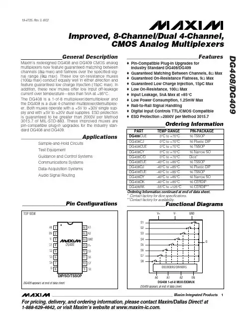
General DescriptionMaxim’s redesigned DG408 and DG409 CMOS analog multiplexers now feature guaranteed matching between channels (8Ωmax) and flatness over the specified sig-nal range (9Ωmax). These low on-resistance muxes (100Ωmax) conduct equally well in either direction and feature guaranteed low charge injection (15pC max). In addition, these new muxes offer low input off-leakage current over temperature—less than 5nA at +85°C. The DG408 is a 1-of-8 multiplexer/demultiplexer and the DG409 is a dual 4-channel multiplexer/demultiplex-er. Both muxes operate with a +5V to +30V single sup-ply and with ±5V to ±20V dual supplies. ESD protection is guaranteed to be greater than 2000V per Method 3015.7 of MI L-STD-883. These improved muxes are pin-compatible plug-in upgrades for the industry stan-dard DG408 and DG409.________________________ApplicationsSample-and-Hold Circuits Test EquipmentGuidance and Control Systems Communications Systems Data-Acquisition Systems Audio Signal Routing____________________________Featureso Pin-Compatible Plug-In Upgrades for Industry Standard DG408/DG409o Guaranteed Matching Between Channels, 8ΩMax o Guaranteed On-Resistance Flatness, 9ΩMax o Guaranteed Low Charge Injection, 15pC Max o Low On-Resistance, 100ΩMax o Input Leakage, 5nA Max at +85°Co Low Power Consumption, 1.25mW Max o Rail-to-Rail Signal Handlingo Digital Input Controls TTL/CMOS Compatible o ESD Protection >2000V per Method 3015.7DG408/DG409Improved, 8-Channel/Dual 4-Channel,CMOS Analog Multiplexers________________________________________________________________Maxim Integrated Products 1Ordering Information_________________Pin Configurations_______________Functional Diagrams19-4725; Rev 3; 8/02*Contact factory for dice specifications.**Contact factory for availability.For pricing, delivery, and ordering information,please contact Maxim/Dallas Direct!at 1-888-629-4642, or visit Maxim’s website at .D G 408/D G 409Improved, 8-Channel/Dual 4-Channel,CMOS Analog Multiplexers 2_______________________________________________________________________________________ABSOLUTE MAXIMUM RATINGSELECTRICAL CHARACTERISTICS —Dual Supplies(V+ = 15V, V- = -15V, GND = 0V, V AH = +2.4V, V AL = +0.8V, T A = T MIN to T MAX , unless otherwise noted.)Stresses beyond those listed under “Absolute Maximum Ratings” may cause permanent damage to the device. These are stress ratings only, and functional operation of the device at these or any other conditions beyond those indicated in the operational sections of the specifications is not implied. Exposure to absolute maximum rating conditions for extended periods may affect device reliability.Voltage Referenced to V-V+............................................................................-0.3V, 44V GND.........................................................................-0.3V, 25V Digital Inputs, S, D (Note 1)....................(V- - 2V) to (V+ + 2V) or30mA, (whichever occurs first)Continuous Current (any terminal)......................................30mA Peak Current, S, D(pulsed at 1ms, 10% duty cycle max)..........................100mAContinuous Power Dissipation (T A = +70°C)TSSOP (derate 9.4mW/°C above +70°C)....................755mW Plastic DIP (derate 10.53mW/°C above +70°C)..........842mW TSSOP (derate 9.4mW/°C above +70°C)....................755mW Narrow SO (derate 8.70mW/°C above +70°C)............696mW CERDIP (derate 10.00mW/°C above +70°C)...............800mW Operating Temperature RangesDG408/DG409C_................................................0°C to +70°C DG408/DG409D,E_.........................................-40°C to +85°C DG408/DG409AK..........................................-55°C to +125°C Storage Temperature Range.............................-65°C to +150°C Lead Temperature (soldering, 10s).................................+300°CNote 1:Signals on S_, D_, EN, A0, A1, or A2 exceeding V+ or V- are clamped by internal diodes. Limit forward current tomaximum current ratings.DG408/DG409Improved, 8-Channel/Dual 4-Channel,CMOS Analog Multiplexers_______________________________________________________________________________________3ELECTRICAL CHARACTERISTICS —Dual Supplies (continued)(V+ = 15V, V- = -15V, GND = 0V, V AH = +2.4V, V AL = +0.8V, T A = T MIN to T MAX , unless otherwise noted.)D G 408/D G 409Improved, 8-Channel/Dual 4-Channel,CMOS Analog Multiplexers 4_______________________________________________________________________________________ELECTRICAL CHARACTERISTICS —Single Supply(V+ = 12V, V- = 0V, GND = 0V, V AH = +2.4V, V AL = +0.8V, T A = T MIN to T MAX , unless otherwise noted.)Note 2:The algebraic convention where the most negative value is a minimum and the most positive value a maximum is used inthis data sheet.Note 3:Guaranteed by design.Note 4:∆R ON = R ON(MAX)- R ON(MIN).On-resistance match between channels and flatness are guaranteed only with specifiedvoltages. Flatness is defined as the difference between the maximum and minimum value of on-resistance as measured at the extremes of the specified analog signal range.Note 5:Leakage parameters are 100% tested at the maximum rated hot temperature and guaranteed by correlation at +25°C.Note 6:Off isolation = 20log V D /V S , where V D = output and V S = input to off switch.DG408/DG409Improved, 8-Channel/Dual 4-Channel,CMOS Analog Multiplexers_______________________________________________________________________________________5120140160ON-RESISTANCE vs. V D (DUAL SUPPLIES)1000204060-2020-1515-1010-55080V D (V)r D S (O N ) (Ω)120ON-RESISTANCE vs. V D ANDTEMPERATURE (DUAL SUPPLIES)1000204060-1515-1010-55080V D (V)r D S (O N ) (Ω)280320360400ON-RESISTANCE vs. V D (SINGLE SUPPLY)24040801201601520105200V D (V)r D S (O N ) (Ω)120140160ON-RESISTANCE vs. V D AND TEMPERATURE (SINGLE SUPPLY)10002040601510580V D (V)r D S (O N ) (Ω)30CHARGE INJECTION vs. V D20-30-20-100-1515-1010-55010V D (V)Q j (p C )100.0001-55125OFF LEAKAGE vs. TEMPERATURE1TEMPERATURE (°C)O F F L E A K A G E (n A )250.010.001-35-15650.1100100045851055100.0001-55125ON LEAKAGE vs. TEMPERATURE1TEMPERATURE (°C)O N L E A K A G E (n A )250.010.001-35-15650.11001000458510551000.001-55125SUPPLY CURRENT vs. TEMPERATURE10TEMPERATURE (°C)I +, I - (µA )250.10.01-35-1565145851055__________________________________________Typical Operating Characteristics(T A = +25°C, unless otherwise noted.)__________Applications InformationOperation withSupply Voltages Other than 15VUsing supply voltages less than ±15V reduces the ana-log signal range. The DG408/DG409 switches operate with ±5V to ±20V bipolar supplies or with a +5V to +40V single supply. Connect V- to GND when operat-ing with a single supply. Both device types can also operate with unbalanced supplies, such as +24V and -5V. The Typica l Opera ting Cha ra cteristics graphs show typical on-resistance with 20V, 15V, 10V, and 5V supplies. (Switching times increase by a factor of two or more for operation at 5V.)Overvoltage ProtectionProper power-supply sequencing is recommended for all CMOS devices. Do not exceed the absolute maxi-mum ratings, because stresses beyond the listed rat-ings may cause permanent damage to the devices.Always sequence V+ on first, then V-, followed by the logic inputs, S or D. If power-supply sequencing is not possible, add two small signal diodes in series with supply pins for overvoltage protection (Figure 1).Adding diodes reduces the analog signal range to 1V below V+ and 1V above V-, but does not affect the devices’ low switch resistance and low leakage charac-teristics. Device operation is unchanged, and the differ-ence between V+ and V- should not exceed +44V.D G 408/D G 409Improved, 8-Channel/Dual 4-Channel,CMOS Analog Multiplexers 6_____________________________________________________________________________________________________________________________________________________Pin DescriptionFigure 1. Overvoltage Protection Using External Blocking DiodesPINDG408DG409NAME FUNCTION1, 15, 16A0, A2, A1Address Inputs ——A0, A1Address Inputs 22EN Enable Input33V-Negative Supply Voltage Input 4–7—S1–S4Bidirectional Analog Inputs —4–7S1A–S4ABidirectional Analog Inputs 8—D Bidirectional Analog Output —8, 9DA, DB Bidirectional Analog Outputs 9–12—S8–S5Bidirectional Analog Inputs —10–13S4B–S1B Bidirectional Analog Inputs 1314V+Positive Supply Voltage Input 1415GNDGround1, 16DG408/DG409Improved, 8-Channel/Dual 4-Channel,CMOS Analog Multiplexers_______________________________________________________________________________________7______________________________________________Test Circuits/Timing DiagramsFigure 2. Transition TimeD G 408/D G 409Improved, 8-Channel/Dual 4-Channel,CMOS Analog Multiplexers 8________________________________________________________________________________________________________________________Test Circuits/Timing Diagrams (continued)Figure 5. Charge InjectionDG408/DG409Improved, 8-Channel/Dual 4-Channel,CMOS Analog Multiplexers_______________________________________________________________________________________9_________________________________Test Circuits/Timing Diagrams (continued)Figure 6. Off-Isolation Figure 7. CrosstalkFigure 8. Source/Drain CapacitanceD G 408/D G 409Improved, 8-Channel/Dual 4-Channel,CMOS Analog Multiplexers 10______________________________________________________________________________________Pin Configurations/Functional Diagrams/Truth Tables (continued)DG408/DG409Improved, 8-Channel/Dual 4-Channel,CMOS Analog Multiplexers______________________________________________________________________________________11Ordering Information (continued)**Contact factory for availability.Package InformationFor the latest package outline information, go to /packages .D G 408/D G 409Improved, 8-Channel/Dual 4-Channel,CMOS Analog Multiplexers __________________________________________________________Chip TopographiesS40.080"(2.03mm)D S8S7S4A 0.080"(2.03mm)DA DB S4BTRANSISTOR COUNT: 122SUBSTRATE CONNECTED TO V+TRANSISTOR COUNT: 122SUBSTRATE CONNECTED TO V+DG408DG409N.C. = NO INTERNAL CONNECTIONMa xim ca nnot a ssume responsibility for use of a ny circuitry other tha n circuitry entirely embodied in a Ma xim product. No circuit pa tent licenses a re implied. Maxim reserves the right to change the circuitry and specifications without notice at any time.12____________________Maxim Integrated Products, 120 San Gabriel Drive, Sunnyvale, CA 94086 408-737-7600©2002 Maxim Integrated ProductsPrinted USAis a registered trademark of Maxim Integrated Products.。