基本逻辑门课件
- 格式:ppt
- 大小:691.00 KB
- 文档页数:30

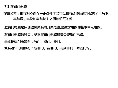
Digital FundamentalsLogic gatesObjectives∙Describe the operation of the inverter, the AND gate, and the OR gate∙Describe the operation of the NAND gate and the NOR gate∙Express the operation of the NOT, AND, OR, NAND, and NOR gates with Booleanalgebra∙Describe the operation of the exclusive-OR and exclusive-NOR gates∙Recognize and use both the distinctive shape logic gate symbols and the rectangularoutline logic gate symbols of ANSI/IEEE Standard 91-1984∙Construct timing diagrams showing the proper time relationships of inputs and outputsfor the various logic gates∙Make basic comparisons between the major IC technologies -CMOS and TTL∙Explain how the different series within the CMOS and TTL families differ from each other∙Define propagation, delay time, power dissipation, speed-power product, and fan-out inrelation to logic gates∙List specific fixed-function integrated circuit devices that contain the various logic gates∙Use each logic gate in simple applications∙Troubleshoot logic gates for opens and shorts by using the logic pulser and probe or theoscilloscope∙Describe the basic concepts of programmable logicInverterCheck out the file F03-02!Thruth tableAND GatePulsed operationLogic expressions for an AND gateEnable/inhibit function with an AND gate AND works as a gate for the clock signalSeat belt alarm systemOR GateLogic expressions for an OR gate0 + 0 = 00 + 1 = 11 + 0 = 11 + 1 = 1Simplified intrusion detectionNAND GateEquivalent operations!ExampleExampleNOR GateEquivalent operations!ExamplePulsed operationExampleFixed-function logic: IC gates5V3V3Fixed-function logic gates -ExamplesIC packagesPin configuration diagrams for some common fixed-function ICsLogic symbols for hex inverterPerformance characteristics and parameterspropagation delay timePLHPHL t and tDC Supply voltage (marked V CC )With CMOS gates you can use wider supply voltage range:5V CMOS tolerates supply variations from 2V to 6V ,3V3 CMOS tolerates supply variations from 2V to 3.6VTTL requires stable supply voltage: maximum variationis +/-10% (i.e. 4.5V to 5.5V)Power dissipation (marked P D )⎪⎭⎫ ⎝⎛+=2CCL CCH CC D I I V P supply current withHIGH ouputsupply current withLOW ouputCMOS power dissipation is usually smaller compared to TTL, but the dissipationdepends on frequency (power dissipation for TTL has no frequency dependence).Input and output logic levels5V CMOS 1.5V 3.5V 5V CMOS 0.33V 4.4V TTL 0.8V 2V TTL0.4V 2.4VSpeed-power product (SPP)DP P t SPP can be used to compared devices when considering both the speed and the dissipation powerFan-out and loadingFan-out is the number of inputs (of the same IC family) that can be connected to its output and still mantain the output voltage levels within specified limits.In CMOS circuits the fan-out is high but depends on frequency thru capacitive effectsComparison of propagation delay time and power in CMOS and TTLHow to read datasheets and find the information you needTroubleshootingInternal failures –An open TTL input acts as a HIGH levelExampleExampleExampleProgrammable arrays –OR arrayProgrammable arrays –AND arrayClassification of SPLDs –PROMClassification of SPLDs –PLA (programmable logic array)。