S-817A35中文资料
- 格式:pdf
- 大小:420.71 KB
- 文档页数:23
Absolute Maximum Ratings
Table 3 Absolute Maximum Ratings (Ta=25C unless otherwise specified)
Item Input voltage Output voltage Power dissipation Operating temperature range Storage temperature range
元器件交易网
Rev.1.1
ULTRA COMPACT CMOS VOLTAGE REGULATOR S-817 Series
The S-817 is an ultra compact 3-pin positive voltage regulator developed using CMOS technology. Due to housing into an even more miniaturized SC-82AB package of 2.0 x 2.1 mm, the S-817 offers key advantages for small, portable applications. The S-817 allows many type of output capacitors including a ceramic type and ensures highly-stable operations at low load of 1µA.
0.18 0.27
V
1
5.0V ≤ VOUT(S) ≤ 5.4V −
0.16 0.25
V
1
5.5V ≤ VOUT(S) ≤ 6.0V −
0.15 0.23
V
1
Line regulation 1
∆ VOUT11 VOUT(S) + 1 V ≤ VIN ≤ 10 V,
−
5
20
mV
1
IOUT = 1mA
0.40 0.67
V
1
2.5V ≤ VOUT(S) ≤ 2.9V −
0.31 0.51
V
1
3.0V ≤ VOUT(S) ≤ 3.4V −
0.25 0.41
V
1
3.5V ≤ VOUT(S) ≤ 3.9V −
0.22 0.35
V
1
4.0V ≤ VOUT(S) ≤ 4.4V −
0.19 0.30
V
1
4.5V ≤ VOUT(S) ≤ 4.9V −
voltage other than those specified above.
Rev.1.1
Pin Configuration
For details of package, refer to the
attached drawing.
4
3
SC-82AB Top view
1
2
Figure 2 SC-82AB
50 mA capable (3.0 V output product, VIN=5 V) Note1 75 mA capable (5.0 V output product, VIN=7 V) Note1
n Applications
Ÿ Power source for
battery-powered devices Ÿ Power source for
1
× 0.98
× 1.02
Output current
*2)
IOUT
VOUT(S)+2V1.1V ≤ VOUT(S) ≤ 1.9V 20
−
−
mA
3
≤ VIN≤10V 2.0V ≤ VOUT(S) ≤ 2.9V 35
−
−
mA
3
3.0V ≤ VOUT(S) ≤ 3.9V 50
−
−
mA
3
4.0V ≤ VOUT(S) ≤ 4.9V 65
n Features
Ÿ Low current consumption
During operation: Typ. 1.2 µA, Max. 2.5 µA Ÿ Output voltage: 0.1 V steps between 1.1 and 6.0 V Ÿ High accuracy output voltage: ±2.0% Ÿ Output current;
S-817A33ANB-CUW-T2
3.5 V ± 2.0%
S-817A35ANB-CUY-T2
4.0 V ± 2.0%
S-817A40ANB-CVD-T2
4.2 V ± 2.0%
S-817A42ANB-CVF-T2
5.0 V ± 2.0%
S-817A50ANB-CVN-T2
Note:
Contact our sales personnel for products with an output
personal communication devices Ÿ Power source for home electric/electronic
appliances
Ÿ Dropout (VOUT = 5.0 V, IOUT = 10 mA)
Ÿ Low ESR capacitor (e.g., a ceramic capacitor of
−
−
mA
3
5.0V ≤ VOUT(S) ≤ 6.0V 75
−
−
mA
3
Dropout voltage
*3) Vdrop IOUT =
1.1V ≤ VOUT(S) ≤ 1.4V −
0.92 1.58
V
1
10mA
1.5V ≤ VOUT(S) ≤ 1.9V −
0.58 0.99
V
1
2.0V ≤ VOUT(S) ≤ 2.4V −
2
Seiko Instruments Inc.
元器件交易网
Rev.1.1
ULTRA COMPACT CMOS VOLTAGE REGULATOR S-817 Series
n Electrical Characteristics
1. S-817AXXANB Item
Table 4 Electrical Characteristics
元器件交易网
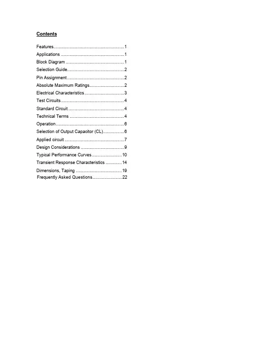
Contents
Features......................................................... 1 Applications ...................................................1 Block Diagram ...............................................1 Selection Guide..............................................2 Pin Assignment ..............................................2 Absolute Maximum Ratings............................2 Electrical Characteristics ................................3 Test Circuits...................................................4 Standard Circuit .............................................4 Technical Terms ............................................4 Operation .......................................................6 Selection of Output Capacitor (CL).................6 Applied circuit ................................................7 Design Considerations ...................................9 Typical Performance Curves ........................ 10 Transient Response Characteristics ............. 14 Dimensions, Taping ..................................... 19 Frequently Asked Questions........................22
VSS
Note 2 Parasitic diode
Figure 1 Block Diagram
Seiko Instruments Inc.
1
元器件交易网
ULTRA COMPACT CMOS VOLTAGE REGULATOR S-817 Series
Selection Guide
0.1 µF or more) can be used as the output capacitor. Ÿ Built-in short current limit circuit
Ÿ Excellent Line Regulation: Stable operation at low
load of 1µA Ÿ Ultra compact package: SC-82AB
Output Voltage
SC-82AB