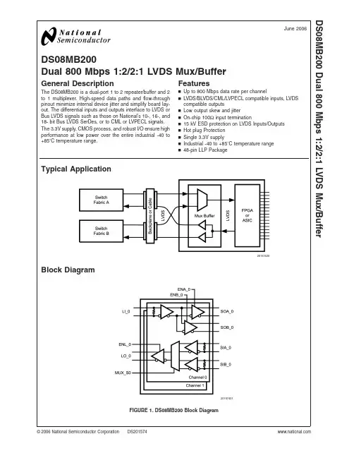
DS08MB200Dual 800Mbps 1:2/2:1LVDS Mux/BufferGeneral DescriptionThe DS08MB200is a dual-port 1to 2repeater/buffer and 2to 1multiplexer.High-speed data paths and flow-through pinout minimize internal device jitter and simplify board lay-out.The differential inputs and outputs interface to LVDS or Bus LVDS signals such as those on National’s 10-,16-,and 18-bit Bus LVDS SerDes,or to CML or LVPECL signals.The 3.3V supply,CMOS process,and robust I/O ensure high performance at low power over the entire industrial -40to +85˚C temperature range.Featuresn Up to 800Mbps data rate per channeln LVDS/BLVDS/CML/LVPECL compatible inputs,LVDS compatible outputsn Low output skew and jittern On-chip 100Ωinput terminationn 15kV ESD protection on LVDS Inputs/Outputs n Hot plug Protection n Single 3.3V supplyn Industrial -40to +85˚C temperature range n 48-pin LLP PackageTypical Application20157420Block Diagram20157401FIGURE 1.DS08MB200Block DiagramJune 2006DS08MB200Dual 800Mbps 1:2/2:1LVDS Mux/Buffer©2006National Semiconductor Corporation Pin DescriptionsPin Name LLP Pin Number I/O,TypeDescriptionSWITCH SIDE DIFFERENTIAL INPUTSSIA_0+SIA_0−3029I,LVDS Switch A-side Channel 0inverting and non-inverting differential inputs.LVDS,Bus LVDS,CML,or LVPECL compatible.SIA_1+SIA_1−1920I,LVDS Switch A-side Channel 1inverting and non-inverting differential inputs.LVDS,Bus LVDS,CML,or LVPECL compatible.SIB_0+SIB_0−2827I,LVDS Switch B-side Channel 0inverting and non-inverting differential inputs.LVDS,Bus LVDS,CML,or LVPECL compatible.SIB_1+SIB_1−2122I,LVDSSwitch B-side Channel 1inverting and non-inverting differential inputs.LVDS,Bus LVDS,CML,or LVPECL compatible.LINE SIDE DIFFERENTIAL INPUTSLI_0+LI_0−4039I,LVDS Line-side Channel 0inverting and non-inverting differential inputs.LVDS,Bus LVDS,CML,or LVPECL compatible.LI_1+LI_1−910I,LVDSLine-side Channel 1inverting and non-inverting differential inputs.LVDS,Bus LVDS,CML,or LVPECL compatible.SWITCH SIDE DIFFERENTIAL OUTPUTSSOA_0+SOA_0−3433O,LVDS Switch A-side Channel 0inverting and non-inverting differential outputs.LVDS compatible(Notes 1,3).SOA_1+SOA_1−1516O,LVDS Switch A-side Channel 1inverting and non-inverting differential outputs.LVDS compatible(Notes 1,3).SOB_0+SOB_0−3231O,LVDS Switch B-side Channel 0inverting and non-inverting differential outputs.LVDS compatible(Notes 1,3).SOB_1+SOB_1−1718O,LVDS Switch B-side Channel 1inverting and non-inverting differential outputs.LVDS compatible(Notes 1,3).LINE SIDE DIFFERENTIAL OUTPUTSLO_0+LO_0−4241O,LVDS Line-side Channel 0inverting and non-inverting differential outputs.LVDS compatible (Notes1,3).LO_1+LO_1−78O,LVDS Line-side Channel 1inverting and non-inverting differential outputs.LVDS compatible (Notes1,3).DIGITAL CONTROL INTERFACEMUX_S0MUX_S13811I,LVTTL Mux Select Control Inputs (per channel)to select which Switch-side input,A or B,is passed through to the Line-side.ENA_0ENA_1ENB_0ENB_136133514I,LVTTLOutput Enable Control for Switch A-side and B-side outputs.Each output driver on the A-side and B-side has a separate enable pin.ENL_0ENL_1454I,LVTTLOutput Enable Control for The Line-side outputs.Each output driver on the Line-side has a separate enable pin.POWER V DD 6,12,37,43,48I,Power V DD =3.3V ±0.3V.GND2,3,46,47(Note 2)I,PowerGround reference for LVDS and CMOS circuitry.For the LLP package,the DAP is used as the primary GND connection to the device.The DAP is the exposed metal contact at the bottom of the LLP-48package.It should beconnected to the ground plane with at least 4vias for optimal AC and thermal performance.N/C1,5,23,24,25,26,44No ConnectNote 1:For interfacing LVDS outputs to CML or LVPECL compatible inputs,refer to the applications section of this datasheet.Note 2:Note that the DAP on the backside of the LLP package is the primary GND connection for the device when using the LLP package.Note 3:The LVDS outputs do not support a multidrop (BLVDS)environment.The LVDS output characteristics of the DS08MB200device have been optimized for point-to-point backplane and cable applications.D S 08M B 200 2Connection Diagrams20157402 Top ViewDAP=GND20157403 Directional Signal Paths Top View (Refer to pin names for signal polarity)TRI-STATE and Powerdown Modes The DS08MB200has output enable control on each of the six onboard LVDS output drivers.This control allows each output individually to be placed in a low power TRI-STATE mode while the device remains active,and is useful to reduce power consumption on unused channels.In TRI-STATE mode,some outputs may remain active while some are in TRI-STATE.When all six of the output enables(all drivers on both chan-nels)are deasserted(LOW),then the device enters a Pow-erdown mode that consumes only0.5mA(typical)of supply current.In this mode,the entire device is essentially pow-ered off,including all receiver inputs,output drivers and internal bandgap reference generators.When returning to active mode from Powerdown mode,there is a delay until valid data is presented at the outputs because of the ramp to power up the internal bandgap reference generators.Any single output enable that remains active will hold the device in active mode even if the other five outputs are in TRI-STATE.When in Powerdown mode,any output enable that becomes active will wake up the device back into active mode,even if the other five outputs are in TRI-STATE.Input Failsafe BiasingExternal pull up and pull down resistors may be used to provide enough of an offset to enable an input failsafe under open-circuit conditions.This configuration ties the positive LVDS input pin to VDD thru a pull up resistor and the negative LVDS input pin is tied to GND by a pull down resistor.The pull up and pull down resistors should be in the 5kΩto15kΩrange to minimize loading and waveform dis-tortion to the driver.Please refer to application note AN-1194,“Failsafe Biasing of LVDS Interfaces”for more infor-mation.Output CharacteristicsThe output characteristics of the DS08MB200have beenoptimized for point-to-point backplane and cable applica-tions,and are not intended for multipoint or multidrop signal-ing.Multiplexer Truth Table(Note4)Data Inputs Control Inputs Output SIA_0SIB_0MUX_S0ENL_0LO_0X valid01SIB_0valid X11SIA_0X X X0(Note5)Z X=Don’t CareZ=High Impedance(TRI-STATE)Repeater/Buffer Truth Table(Note4)DataInput Control Inputs OutputsLI_0ENA_0ENB_0SOA_0SOB_0X00Z(Note5)Z(Note5)valid01Z LI_0valid10LI_0Zvalid11LI_0LI_0 X=Don’t CareZ=High Impedance(TRI-STATE)Note4:Same functionality for channel1Note5:When all enable inputs from both channels are Low,the deviceenters a powerdown mode.Refer to the applications section titled TRI-STATEand Powerdown modes.DS08MB2003Absolute Maximum Ratings (Note 6)Supply Voltage (V DD )−0.3V to +4.0V CMOS Input Voltage -0.3V to (V DD +0.3V)LVDS Receiver Input Voltage (Note 7)-0.3V to (V DD +0.3V)LVDS Driver Output Voltage -0.3V to (V DD +0.3V)LVDS Output Short Circuit Current +40mA Junction Temperature +150˚CStorage Temperature−65˚C to +150˚CLead Temperature (Solder,4sec)260˚C Max Pkg Power Capacity @25˚C 5.2W Thermal Resistance (θJA )24˚C/W Package Derating above +25˚C 41.7mW/˚CESD Last Passing Voltage HBM,1.5k Ω,100pF 8kV LVDS pins to GND only15kVEIAJ,0Ω,200pF 250V CDM1000VRecommended Operating ConditionsSupply Voltage (V CC ) 3.0V to 3.6V Input Voltage (V I )(Note 7)0V to V CC Output Voltage (V O )0V to V CCOperating Temperature (T A )Industrial−40˚C to +85˚C Note 6:Absolute maximum ratings are those values beyond which damage to the device may occur.The databook specifications should be met,without exception,to ensure that the system design is reliable over its power supply,temperature,and output/input loading variables.National does not recom-mend operation of products outside of recommended operation conditions.Note 7:V ID max <2.4VElectrical CharacteristicsOver recommended operating supply and temperature ranges unless other specified.SymbolParameterConditionsMinTyp (Note 8)MaxUnitsLVTTL DC SPECIFICATIONS (MUX_Sn,ENA_n,ENB_n,ENL_n)V IH High Level Input Voltage 2.0V DD V V IL Low Level Input Voltage GND 0.8V I IH High Level Input Current V IN =V DD =V DDMAX −10+10µA I IL Low Level Input Current V IN =V SS ,V DD =V DDMAX −10+10µA C IN1Input Capacitance Any Digital Input Pin to V SS 3.5pF C OUT1Output Capacitance Any Digital Output Pin to V SS 5.5pF V CL Input Clamp VoltageI CL =−18mA−1.5−0.8VLVDS INPUT DC SPECIFICATIONS (SIA ±,SIB ±,LI ±)V TH Differential Input High Threshold (Note 9)V CM =0.8V or 1.2V or 3.55V,V DD =3.6V0100mV V TL Differential Input Low Threshold (Note 9)V CM =0.8V or 1.2V or 3.55V,V DD =3.6V−1000mV V ID Differential Input Voltage V CM =0.8V to 3.55V,V DD =3.6V 1002400mV V CMR Common Mode Voltage Range V ID =150mV,V DD =3.6V 0.053.55V C IN2Input Capacitance IN+or IN−to V SS3.5pF I INInput CurrentV IN =3.6V,V DD =V DDMAX −15+15µA V IN =0V,V DD =V DDMAX−15+15µALVDS OUTPUT DC SPECIFICATIONS (SOA_n ±,SOB_n ±,LO_n ±)V OD Differential Output Voltage,(Note 9)R L is the internal 100Ωbetween OUT+and OUT−250360500mV ∆V OD Change in V OD between Complementary States -3535mV V OS Offset Voltage (Note 10) 1.05 1.22 1.475V ∆V OS Change in V OS between Complementary States -3535mV I OS Output Short Circuit Current OUT+or OUT−Short to GND −21-40mA C OUT2Output CapacitanceOUT+or OUT−to GND when TRI-STATE5.5pFD S 08M B 200 4Electrical Characteristics(Continued)Over recommended operating supply and temperature ranges unless other specified.Symbol Parameter Conditions MinTyp(Note8)Max UnitsSUPPLY CURRENT(Static)I CC Supply Current All inputs and outputs enabled andactive,terminated with differential loadof100Ωbetween OUT+and OUT-.225275mAI CCZ Supply Current-PowerdownMode ENA_0=ENB_0=ENL_0=ENA_1=ENB_1=ENL_1=L0.6 4.0mASWITCHING CHARACTERISTICS—LVDS OUTPUTSt LHT Differential Low to High Transition Time Use an alternating1and0pattern at200Mb/s,measure between20%and80%of V OD.(Note15)170250pst HLT Differential High to Low TransitionTime170250pst PLHD Differential Low to HighPropagation Delay Use an alternating1and0pattern at200Mb/s,measure at50%V ODbetween input to output.1.02.5nst PHLD Differential High to LowPropagation Delay1.02.5ns t SKD1Pulse Skew|t PLHD–t PHLD|(Note15)2575ps t SKCC Output Channel to Channel Skew Difference in propagation delay(t PLHDor t PHLD)among all output channels.(Note15)50115pst JIT Jitter(Note11)RJ-Alternating1and0at400MHz(Note12)1.3 1.5psrms DJ-K28.5Pattern,800Mbps(Note13)1534psp-p TJ-PRBS27-1Pattern,800Mbps(Note14)1634psp-pt ON LVDS Output Enable Time Time from ENA_n,ENB_n,or ENL_n toOUT±change from TRI-STATE toactive.0.5 1.5µst ON2LVDS Output Enable time frompowerdown mode Time from ENA_n,ENB_n,or ENL_n toOUT±change from Powerdown toactive1020µst OFF LVDS Output Disable Time Time from ENA_n,ENB_n,or ENL_n toOUT±change from active toTRI-STATE or powerdown.12nsNote8:Typical parameters are measured at V DD=3.3V,T A=25˚C.They are for reference purposes,and are not production-tested.Note9:Differential output voltage V OD is defined as ABS(OUT+–OUT−).Differential input voltage V ID is defined as ABS(IN+–IN−).Note10:Output offset voltage V OS is defined as the average of the LVDS single-ended output voltages at logic high and logic low states.Note11:Jitter is not production tested,but guaranteed through characterization on a sample basis.Note12:Random Jitter,or RJ,is measured RMS with a histogram including1500histogram window hits.The input voltage=V ID=500mV,50%duty cycle at400 MHz,t r=t f=50ps(20%to80%).Note13:Deterministic Jitter,or D J,is measured to a histogram mean with a sample size of350hits.Stimulus and fixture jitter has been subtracted.The input voltage=V ID=500mV,K28.5pattern at800Mbps,t r=t f=50ps(20%to80%).The K28.5pattern is repeating bit streams of(00111110101100000101).Note14:Total Jitter,or T J,is measured peak to peak with a histogram including3500window hits.Stimulus and fixture jitter has been subtracted.The input voltage =V ID=500mV,27-1PRBS pattern at800Mbps,t r=t f=50ps(20%to80%).Note15:Not production tested.Guaranteed by statistical analysis on a sample basis at the time of characterization.DS08MB2005Typical Performance CharacteristicsPower Supply Current vs.Bit Data RateTotal Jitter vs.Temperature20157412Dynamic power supply current was measured with all channels active and toggling at the bit data rate.Data pattern has no effect on the power consumption.V DD =3.3V,T A =+25˚C,V ID =0.5V,V CM =1.2V.20157410Total Jitter measured at 0V differential while running a PRBS 27-1pattern with one channel active,all other channels are disabled.V DD =3.3V,V ID =0.5V,V CM =1.2V,800Mbps data rate.Stimulus and fixture jitter has been subtracted.Total Jitter vs.Bit Data Rate20157411Total Jitter measured at 0V differential while running a PRBS 27-1pattern with one channel active,all other channels are disabled.V DD =3.3V,T A =+25˚C,V ID =0.5V.Stimulus and fixture jitter has been subtracted.D S 08M B 200 6Interfacing LVPECL to LVDSAn LVPECL driver consists of a differential pair with coupled emitters connected to GND via a current source.This drives a pair of emitter-followers that require a50ohm to V CC-2.0 load.A modern LVPECL driver will typically include the ter-mination scheme within the device for the emitter follower.If the driver does not include the load,then an external scheme must be used.The 1.3V supply is usually not readily available on a PCB,therefore,a load scheme without a unique power supply requirement may be used.Figure2is a separatedπtermination scheme for a3.3V LVPECL driver.R1and R2provides proper DC load for the driver emitter followers,and may be included as part of the driver device(Note16).The DS08MB200includes a100 ohm input termination for the transmission line.The common mode voltage will be at the normal LVPECL levels–around 2V.This scheme works well with LVDS receivers that have rail-to-rail common mode voltage,V CM,range.Most National Semiconductor LVDS receivers have wide V CM range.The exceptions are noted in devices’respective datasheets. Those LVDS devices that do have a wide V CM range do not vary in performance significantly when receiving a signal with a common mode other than standard LVDS V CM of1.2 V.An AC coupled interface is preferred when transmitter and receiver ground references differ more than1V.This is a likely scenario when transmitter and receiver devices are on separate PCBs.Figure3illustrates an AC coupled interface between a LVPECL driver and LVDS receiver.R1and R2,if not present in the driver device(Note16),provide DC load for the emitter followers and may range between140-220 ohms for most LVPECL devices for this particular configura-tion.The DS08MB200includes an internal100ohm resistor to terminate the transmission line for minimal reflections.The signal after ac coupling capacitors will swing around a level set by internal biasing resistors(i.e.fail-safe)which is either V DD/2or0V depending on the actual failsafe implementa-tion.If internal biasing is not implemented,the signal com-mon mode voltage will slowly wander to GND level.Interfacing LVDS to LVPECLAn LVDS driver consists of a current source(nominal3.5mA) which drives a CMOS differential pair.It needs a differential resistive load in the range of70to130ohms to generate LVDS levels.In a system,the load should be selected to match transmission line characteristic differential impedance so that the line is properly terminated.The termination resis-tor should be placed as close to the receiver inputs as possible.When interfacing an LVDS driver with a non-LVDS receiver,one only needs to bias the LVDS signal so that it is within the common mode range of the receiver.This may be done by using separate biasing voltage which demands another power supply.Some receivers have required biasing voltage available on-chip(V T,V TT or V BB).Figure4illustrates interface between an LVDS driver and a LVPECL with a V T pin available.R1and R2,if not present in the receiver(Note16),provide proper resistive load for the driver and termination for the transmission line,and V T sets desired bias for the receiver.Figure5illustrates AC coupled interface between an LVDS driver and LVPECL receiver without a V T pin available.The resistors R1,R2,R3,and R4,if not present in the receiver (Note16),provide a load for the driver,terminate the trans-mission line,and bias the signal for the receiver.Note16:The bias networks shown above for LVPECL drivers and receivers may or may not be present within the driver device.The LVPECL driver and receiver specification must be reviewed closely to ensure compatibility be-tween the driver and receiver terminations and common mode operating ranges.20157461 FIGURE2.DC Coupled LVPECL to LVDS Interface20157462 FIGURE3.AC Coupled LVPECL to LVDS Interface20157463 FIGURE4.DC Coupled LVDS to LVPECL Interface20157464 FIGURE5.AC Coupled LVDS to LVPECL InterfaceDS08MB2007Physical Dimensionsinches (millimeters)unless otherwise noted48-Pin LLPNS Package Number SQA48aOrdering Code DS08MB200TSQ (250piece Tape and Reel)DS08MB200TSQX (2500piece Tape and Reel)National does not assume any responsibility for use of any circuitry described,no circuit patent licenses are implied and National reserves the right at any time without notice to change said circuitry and specifications.For the most current product information visit us at .LIFE SUPPORT POLICYNATIONAL’S PRODUCTS ARE NOT AUTHORIZED FOR USE AS CRITICAL COMPONENTS IN LIFE SUPPORT DEVICES OR SYSTEMS WITHOUT THE EXPRESS WRITTEN APPROVAL OF THE PRESIDENT AND GENERAL COUNSEL OF NATIONAL SEMICONDUCTOR CORPORATION.As used herein:1.Life support devices or systems are devices or systems which,(a)are intended for surgical implant into the body,or (b)support or sustain life,and whose failure to perform when properly used in accordance with instructions for use provided in the labeling,can be reasonably expected to result in a significant injury to the user.2.A critical component is any component of a life support device or system whose failure to perform can be reasonably expected to cause the failure of the life support device or system,or to affect its safety or effectiveness.BANNED SUBSTANCE COMPLIANCENational Semiconductor follows the provisions of the Product Stewardship Guide for Customers (CSP-9-111C2)and Banned Substances and Materials of Interest Specification (CSP-9-111S2)for regulatory environmental compliance.Details may be found at:/quality/green.Lead free products are RoHS compliant.National Semiconductor Americas Customer Support CenterEmail:new.feedback@ Tel:1-800-272-9959National SemiconductorEurope Customer Support CenterFax:+49(0)180-5308586Email:europe.support@Deutsch Tel:+49(0)6995086208English Tel:+44(0)8702402171Français Tel:+33(0)141918790National Semiconductor Asia Pacific Customer Support CenterEmail:ap.support@National SemiconductorJapan Customer Support Center Fax:81-3-5639-7507Email:jpn.feedback@ Tel:81-3-5639-7560D S 08M B 200D u a l 800M b p s 1:2/2:1L V D S M u x /B u f f e r。