超低相噪OCXO的相位噪声测量白皮书
- 格式:pdf
- 大小:1.85 MB
- 文档页数:5
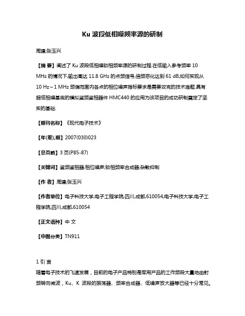
• 92•描述了一种新型恒温晶振(OCXO)的设计方案,在恒温晶振(OCXO)研究基础上,通过对控温电路的优化设计,并采用热敏网络补偿技术,以恒温控制为主,温度补偿为辅,先进行恒温控制,再进行温度补偿。
两者相互结合取得优良的温频特性。
新型恒温晶振的工作电压仅为5V。
其温度-频率特性及相位噪声分别达到≤±1ppb(-40~+70℃)和≤-158dBc/Hz@1kHz的指标。
稳态功耗仅为1.2W,体积为36*27*12.7mm。
引言:石英晶体振荡器是无线电设备的核心部件,是通信、广播、雷达、电子对抗、遥控遥测及许多测量仪器必不可少的部件,其中恒温晶体振荡器(OCXO )是一种频率稳定性最好的高精密晶体振荡器(蒋松涛,一种小型超低相噪恒温晶振的设计:压电与声光,2015)。
大量应用于高端通讯设备中。
目前温频特性要达到10-9~10-11数量级普遍采用双层恒温技术。
存在预热时间长,体积大,功耗高等缺点(赵声衡,晶体振荡器:科学出版社,2008)。
本文描述了一种恒温控制为主,温度补偿为辅,两者相结合的新型OCXO 设计方案。
并成功研制了体积为36×27×12.7(mm ),温度稳定度优于±1×10⁻⁹的小体积低功耗恒温晶振。
1 晶体谐振器温频特性晶体谐振器是一种基于压电效应实现的机械振动系统。
其晶片切型有很多种,包括AT 切、SC 切、BT 切等。
其中比较常用、生产较成熟的是AT 切和SC 切。
SC 切谐振器的显著特点是其频率与温度之间有近似的三次函数关系,因而它具有零温度系数点(John R.Vig Quartz Crystal Resonators and Oscillators For Frequency Control and Timing Applications:U.S.Army Communications-Electronics Command,2001)。
Ku波段低相噪频率源的研制周建;张玉兴【摘要】阐述了Ku波段低相噪锁相频率源的研制过程.在低输入参考频率10 MHz的情况下,输出高达11.8 GHz的点频信号,倍频恶化达到61 dB,如何实现从10 Hz~1 MHz频偏范围内各点的相位噪声指标要求是需要攻克的技术难题.具有超低相噪基底的模拟鉴频鉴相器件HMC440的应用为该项目的成功研制奠定了坚实的基础.【期刊名称】《现代电子技术》【年(卷),期】2007(030)023【总页数】3页(P85-87)【关键词】鉴频鉴相器;相位噪声;锁相频率合成器;杂散抑制【作者】周建;张玉兴【作者单位】电子科技大学,电子工程学院,四川,成都,610054;电子科技大学,电子工程学院,四川,成都,610054【正文语种】中文【中图分类】TN9111 引言随着电子技术的飞速发展,目前的电子产品特别是军用产品的工作频段大量地由射频转向微波,Ku、K波段的振荡器、频率合成器、低噪声放大器等已经十分常见。
作为各种电子系统核心部件的频率合成器(简称频综),虽然有着70多年的发展历史,其理论基础可谓相当完善,但仍然受到实际应用的严峻考验。
目前的频率合成器正朝着模块化、小型化、低功耗、高频谱纯度和多点快速捷变的方向发展。
本文研究的频率合成器是工作在11.8 GHz上的一个点频源,其各项技术指标要求如下:输入频率:10 MHz;输入功率:0 dBm;输出频率:11.8 GHz;输出功率:≥7 dBm;杂波抑制:≥65 dBc;谐波抑制:≥40 dBc。
相位噪声如表1所示。
表1 相位噪声要求10 Hz100 Hz1 kHz10 kHz100 kHz1 MHz-60 dBc/Hz-75-95-100-100-110该项目的难点在于:在低参考输入频率(fref=10 MHz)的情况下,输出高达11.8 GHz的点频信号,并且要同时满足10 Hz~1 MHz频偏范围内比较苛刻的相位噪声指标。
The Effect Of Phase Distortion On InterferometricMeasurements Of Thin Film Coated Optical SurfacesJon Watson, Daniel SavageOptimax Systems, 6367 Dean Parkway, Ontario, NY USA*********************©Copyright Optimax Systems, Inc. 2010This paper discusses difficulty in accurately interpreting surface form data from a phase shifting interferometer measurement of a thin film interference coated surfaces.PHASE-SHIFTING INTERFEROMETRYPhase-shifting interferometry is a metrology tool widely used in optical manufacturing to determine form errors of an optical surface. The surface under test generates a reflected wavefront that interferes with the reference wavefront produced by the interferometer 1. A phase-shifting interferometer modulates phase by slightly moving the reference wavefront with respect to the reflected test wavefront 2 . The phase information collected is converted into the height data which comprises the surface under test3.Visibility of fringes in an interferometer is a function of intensity mismatch between the test and reference beams. Most commercially available interferometers are designed to optimize fringe contrast based on a 4% reflected beam intensity. If the surface under test is coated for minimum reflection near or at the test wavelength of the interferometer, the visibility of the fringe pattern can be too low to accurately measure.OPTICAL THIN-FILM INTERFERENCE COATINGSOptical thin-film interference coatings are structures composed of one or more thin layers (typically multiples of a quarter-wave optical thickness) of materials deposited on the surface of an optical substrate.The goal of interference coatings is to create a multilayer film structure where interference effects within the structure achieve a desired percent intensity transmission or reflection over a given wavelength range.The purpose of the coating defines the design of the multilayer structure. Basic design variables include:• Number of layers• Thickness of each layer• Material of each layerThe most common types of multilayer films are high reflector (HR) and anti-reflection (AR) coatings. HR coatings function by constructively interfering reflected light, while AR coatings function by destructively interfering reflected light. These coatings are designed to operate over a specific wavelength range distributed around a particular design wavelength.To produce the desired interference effects, thin-film structures are designed to modulate the phase of the reflected or transmitted wavefront. The nature of the interference effect depends precisely on the thickness of each layer in the coating as well as the refractive index of each layer. If the thickness and index of each layer is uniform across the coated surface, the reflected wavefront will have a constant phase offset across the surface. However, if layer thicknesses or index vary across the coated surface, then the phase of thereflected wavefront will also vary. Depending on the design of the coating and the severity of the thickness or index non-uniformity, the distortion of the phase of the reflected wavefront can be severe. 4Layer thickness non-uniformity is inherent in the coating process and is exaggerated by increasing radius of curvature of the coated surface.5 All industry-standard directed source deposition processes (thermal evaporation, sputtering, etc) result in some degree of layer thickness non-uniformity.5 Even processes developed to minimize layer non-uniformity, such as those used at Optimax, will still result in slight layer non-uniformity (within design tolerance).TESTING COATED OPTICS INTERFEROMETRICALLYPhase-shifting interferometers use phase information to determine the height map of the surface under test. However, surfaces coated with a thin-film interference coating can have severe phase distortion in the reflected wavefront due to slight layer thickness non-uniformities and refractive index inhomogeneity. Therefore, the measured irregularity of a coated surface measured on a phase shifting interferometer at a wavelength other than the design wavelength, may not represent the actual irregularity of the surface. Even using a phase shifting interferometer at the coating design wavelength does not guarantee accurate surface irregularity measurements. If a coating has very low reflectance over any given wavelength range (such as in the case of an AR coating), the phase shift on reflection with wavelength will vary significantly in that range.7 Figure 1 shows an example of how the phase can vary with coating thickness variations.Figure 1In this particular case, if a point at the lens edge has the nominal coating thickness and the coating at lens center is 2% thicker, expect ~38° phase difference in the measurement (~0.1 waves). This will erroneous be seen as height by the interferometer, despite the actual height change in this case being less than 7nm (~0.01 waves). Also, depending on coating design, low fringe visibility may inhibit measurements.There is an extreme method to determine the irregularity of a thin-film interference coated surface by flash coating it with a bare metal mirror coating. A metal mirror coating is not a thin-film interference coating, and the surface of the mirror represents the true surface, This relatively expensive process requires extra time, handling, and potential damage during the metal coating chemical strip process.CONCLUSIONS•There can be practical limitations to getting accurate surface form data on coated optical surfaces due to issues with phase distortion and fringe visibility.•The issues are a function of thin film coating design particulars and the actual deposition processes.1 R.E. Fischer, B. Tadic-Galeb, P. Yoder, Optical System Design, Pg 340, McGraw Hill, New York City, 20082 H.H. Karow, Fabrication Methods For Precision Optics, Pg 656, John Wiley & Sons, New York City, 19933 MetroPro Reference Guide OMP-0347J, Page 7-1, Zygo Corporation, Middlefield, Connecticut, 20044 H.A. Macleod, Thin Film Optical Filters, Chapter 11: Layer uniformity and thickness monitoring, The Institute of Physics Publishing, 2001.5 R.E. Fischer, B. Tadic-Galeb, P. Yoder, Optical System Design, Pg 581, McGraw Hill, New York City, 2008。
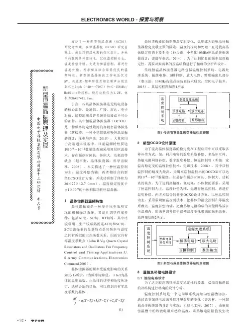
1 恒温晶体振荡器基本原理恒温晶体振荡器简称恒温晶振,英文简称为OCXO(Oven Controlled Crystal Oscillator),是利用恒温槽使晶体振荡器中石英晶体谐振器的温度保持恒定,将由周围温度变化引起的振荡器输出频率变化量削减到最小的晶体振荡器。
OCXO是由恒温槽控制电路和振荡器电路构成的。
通常人们是利用热敏电阻“电桥”构成的差动串联放大器,来实现温度控制。
恒温晶振的基本结构见图1。
2 恒温晶体振荡器的应用领域1)军事和宇航领域:通讯导航、敌我识别器、雷达、传感器、制导系统、引信、电子战、声纳;2)科研与计量:原子钟、测量设备、遥测、遥感、遥控;3)工业领域:通讯、电信、移动/蜂窝/便携式终端、航空、航海、导航、仪器仪表、计算机、数字设备、显示器、磁盘驱动器、调制解调器、标识/认证系统、传感器;4)消费领域:手表与时钟、蜂窝与无绳电话机、普通电话机、呼叫器、音响设备、有线电视系统与电视机、PC、摄象机、业余无线电器材、玩具、医用装置与设备;5)汽车领域:引擎控制,立体声音响时钟,传感器,驾控计算机,GPS应用。
3 恒温晶体振荡器专业术语1)频率准确度:按规定条件要求,在基准温度下测试,晶体振荡器的频率相对于其规定标称值的最大允许偏差,即(f-f0)/f0;2)频率-温度稳定度:按规定条件要求,在规定温度范围内晶体振荡器输出频率的最大变化量相对于温度范围内输出频率极值之和的允许频偏值,即±(fmax-fmin)/(fmax+fmin);3)频率老化:晶体振荡器输出频率随时间的变化,通常用某一时间间隔的频率来量度。
如0至30天的总变化或1年内的预定总频率变化等;4)工作温度范围:振荡器能正常工作。
其频率及其他性能均不超过规定的允许偏差的温度范围;5)稳定时间:振荡器从初始加电到稳定工作在规定极限值所需要的时间;6)相位噪声:是指信号功率与噪声功率的比率(C/N),是表征频率颤抖的技术指标。
晶振电路的生产研发条件质量保证命名规则恒温晶体振荡器(OCXOs)OX253B-H-MR-V-10M OX362D-H-MR-V-10MOX20系列10~40SC±0.01~0.20.2S/T/HOX30x系列10~120SC±0.005~0.20.5S/T/H-140/-14556●●9●1215订购表7●OX14B-T-HU-V-10MOX12A-T-HT-V-40M温度补偿晶体振荡器(TCXOs)TX12/TX14/TX15系列10~120±0.5~512/5/3.3S/T/H/CTXG36B-S-KW-R@300M1922命名规则●-55~+85CTX7A-C-GU-V@10M TX12B-T-JW-N@20M注:ppm=10,120MHz以上为倍频输出,可选定制产品;10MHz以下为分频输出;产品概览8●型号频率范围f(MHz)频率温度稳定度压控频率范围工作电压V输出选择*电压控制晶体振荡器(VCXOs)ppmVX12/VX14/VXM14(SMD)ppm压控线性注:ppm=10, 除VXM15系列外,频率>35MHz压控频率范围为±30ppm; 需宽压控频率范围可选倍频输出。
*:S:Sinewave; LC:L VCMOS; LP:LVPECL。
VXM15B-T-HQ-A@100M页码24命名规则●VX12/VX14/VXM14集成晶体振荡器目录封装外形尺寸图35(TMs )±ppmppm时钟模块概述VTM18B-T-HT-001页码TM18系列±4.62/2CMOS5/3.328±0.370.008~32.768●27集成晶体振荡器目录(XTALs )封装页码29命名规则●±5ppm1、完善的晶体谐振器生产线2 我们拥有1000m 资上千万元完整的晶体谐振器生产线,其主要设备从国外引进,可生产高Q、低老化冷压焊和电阻焊(抽真空)SC、AT切晶体。
gps时钟驯服晶振在南京大学成功案例2017年10月初,西安同步电子科技有限公司自主研发生产的gps 时钟驯服晶振在南京大学投入使用,这套驯服晶振已稳定运行数月,已将我公司纳为合格供应商。
一、时钟驯服晶振简介时钟驯服的基本原理是利用卫星授时接收机提供的固定频率信号,与本地振荡器产生的振荡信号进行比对,获得频率差;再通过对本地振荡器的调节,使振荡频率与卫星的振荡频率基本一致,在频率调整过程中,还需要对本地振荡器的相位进行补偿,使本地振荡器输出的分频秒信号与接收机输出的秒信号差值在一定范围内.卫星授时接收机由于信号传输距离长,易受干扰等特点,其输出的1pps 具有一定的抖动,秒信号包含多种误差成分,如:卫星时钟误差:星历误差:电离层的附加延时误差:对流层的附加延时误差:多路径误差:接收机本身的误差。
采用GPS授时接收机对高稳晶振进行升级改造,研制高精度时间间隔计数器电路,测量GPS平均秒和高稳晶振分频秒之间的时差,采用驯服算法计算晶振的实时准确度,并通过电子频率控制的方式反馈调整高稳晶振的频率信号,从而提高频率信号的准确性和稳定性。
二、GPS驯服晶振利用高精度的时间间隔测量方法测得GPS信号和本地秒信号的相位差,并经计算机处理后转换成频率差,然后通过高稳晶振的压控调谐对高稳晶振输出频率进行调整,由锁相环回路进行控制使高稳晶振锁定到GPS时钟的准确度,从而完成对高稳晶振的驯服校频过程。
对输入本地频标和GPS秒脉冲信号的鉴相,通过高精度时间间隔测量,测量出两信号的相位差,并将转换为电压值。
然后通过压控OCXO端口对高稳晶振进行压控调整,通过锁相环使本地频标锁定到GPS时钟上。
影响误差分析其中主要影响是GPS引入误差。
又可分为以下几方面的误差:1.1与GPS卫星相关的误差1.1卫星星历误差卫星星历误差是指卫星星历给出的卫星空间位置和卫星实际位置间的偏差,由于卫星空间位置是由地面监控系统根据卫星测轨结果计算求得的,所以又称为卫星轨道误差。
vco 相位噪声相关频率VCO相位噪声相关频率VCO(Voltage Controlled Oscillator)是一种电压控制振荡器,常用于无线通信系统中的频率合成器。
在实际应用中,VCO的性能参数之一是相位噪声,它对通信系统的性能有着重要影响。
相位噪声是指VCO输出信号相位的随机变化,它与频率有一定的关系,即相位噪声相关频率。
相位噪声的相关频率是指相位噪声随频率变化的规律。
在VCO中,相位噪声一般由噪声源引起,噪声源包括各种器件的热噪声、1/f 噪声等。
这些噪声源会对VCO的输出信号相位产生影响,从而导致相位噪声的存在。
相位噪声的相关频率可以通过功率谱密度来表示。
功率谱密度是将相位噪声的能量在频率上的分布进行描述的一种方式。
对于VCO而言,相位噪声的功率谱密度通常被建模为一个随频率增加而增加的函数。
具体来说,VCO的相位噪声功率谱密度可以分为两个部分:高频段和低频段。
在高频段,相位噪声功率谱密度随频率的增加而增加。
这是由于VCO中的噪声源所引起的高频噪声对相位噪声的贡献较大。
而在低频段,相位噪声功率谱密度随频率的减小而减小。
这是由于1/f噪声等低频噪声对相位噪声的贡献较大。
在VCO设计和应用中,相位噪声相关频率是一个重要的参数。
它可以用来评估VCO的性能,并对VCO在无线通信系统中的应用进行优化。
相位噪声相关频率越低,意味着VCO在更低的频率范围内具有较好的相位噪声性能。
这对于要求高稳定性和低相位噪声的通信系统来说尤为重要。
为了降低VCO的相位噪声相关频率,可以采取一些措施。
例如,优化VCO的电路结构,减小噪声源的影响;改善VCO的供电和接地结构,减少电源噪声对VCO的干扰;采用合适的滤波器和稳压电路,降低噪声在VCO电路中的传播和放大等。
这些措施可以有效地降低VCO的相位噪声相关频率,提高VCO的性能。
VCO的相位噪声相关频率是评估VCO性能的重要指标之一。
它对于无线通信系统的稳定性和性能有着重要影响。

2~18 GHz超宽带低噪声放大器芯片研制文晓敏;李斌【摘要】低噪声放大器在射电天文望远镜接收机中是一个重要的前端组件,其性能对接收机的灵敏度和噪声有至关重要的影响。
采用OMMIC公司70 nm GaAs mHEMT工艺研究和设计了一款工作频率为2~18 GHz的超宽带单片微波集成低噪声放大器芯片,芯片面积为2 mm×1 mm。
放大器电路采用三级级联放大、双电源供电拓扑结构,常温在片测试结果显示,全频带增益大于28 dB,噪声温度平均值为93 K,直流功耗150 mW,无条件稳定。
该放大器芯片覆盖了射电天文S,C,X,Ku 4个传统观测波段,适用于厘米波段超宽带接收前端和毫米波段超宽带中频放大模块。
【期刊名称】《天文研究与技术-国家天文台台刊》【年(卷),期】2019(16)3【总页数】7页(P278-284)【关键词】低噪声放大器;GaAs;mHEMT;超宽带;单片微波集成电路【作者】文晓敏;李斌【作者单位】中国科学院上海天文台,上海200030;中国科学院大学,北京100049【正文语种】中文【中图分类】TN722.3作为射电天文望远镜接收机前端的核心器件,低噪声放大器(Low Noise Amplifier, LNA)不仅要将天线接收到的来自外太空的微弱信号进行低噪声放大,还要求具有较高的增益抑制后级链路的噪声,保持接收系统的灵敏度。
单片微波集成电路(Monolithic Microwave Integrated Circuits, MMIC)形式的低噪声放大器芯片是实现超宽带、低噪声、高增益器件的重要途径。
变组分高电子迁移率晶体管(Metamorphic High-eletron-mobility Transistor, mHEMT) 具有高频、高功率及噪声性能好的优点,广泛应用于雷达、遥感、辐射测量等领域[1]。
本文设计单片微波集成电路低噪声放大器芯片所用的OMMIC D007IH mHEMT工艺,拥有70 nm栅长和高掺铟沟道,在组分缓变的缓冲层上生长高铟浓度的外延活跃层,从而实现与砷化镓(GaAs)衬底的平稳过渡,因而使其具有极低的噪声和超高频特性[2]。
微波超低相噪光电振荡器的实验研究方立军;柳勇;马骏;郭雪锋;桂勇锋;吴彭生【摘要】Microwave photonics will make a great impact on radar technology in future.OEO(opto-elec-tronic oscillator)is a novel promising high quality microwave signal generator.It will be a breakthrough in oscillator region.The working theory of OEO is analyzed.The results show that the low noise components, the high loop gain,and long group delay are the effective methods to design a low phase noise OEO.The ex-perimental results of a dual-loop X-band low phase noise OEO aregiven.The results are compared with that of high quality electronic frequency synthesizer and international advanced OEO.The conclusion is that the noise floor of OEO is superior to the traditional electronic frequency synthesizer.But the OEO doesn’t have advantage in close-in carrier phase noise.The reason is that the OEO’s parameters have large drifts with temperature.Future technology development route is discussed and expected.%微波光子学将对未来雷达技术发展产生重要影响。
频综设计方案项目名称:频综方案拟制:批准:年月日一.设计任务1.1电源特性要求工作电源: 5V,电源误差:≤±5%工作电源: 12V,电源误差:≤±10%1.2 插座接口定义图5 J30J-15ZK连接器插座接口定义2.结构指标见图二.方案设计1.产品框图图12.方案原理由100M晶振(0dBm)和由外部数据产生的频率控制字加载到直接频率合成器DDS,使DDS产生49.25MHz-50MHz 步进为62.5HZ的信号(10dBm),然后通过低通滤波及衰减网络使功率降到2dBm满足相位比较器的输入功率在±5dBm之间的要求和滤除高端的杂波,再通过由相位比较,有源环路滤波器和电调振荡器构成的锁相环使之锁定在要跳的频率上,然后通过倍频器使之达到所要求的频率,最后通过带通滤波器进一步滤除杂波输出19.85GHz±150MHz 步进为25KHz 功率为10dBm的信号。
参考时钟要求:为达到相位噪声要求采用高稳定低相噪的OCXO系列晶振,满足参考时钟的技术指标100M±0.05ppm,相噪:-135 dBc/Hz@1kHz。
系统相位噪声要求:如上表所示晶振的相噪:-135 dBc/Hz@1kHz 而整数分频N=100,20㏒N=40再通过两次倍频相噪变差6dB,系统相噪=-135+40+6=-89 dBc/Hz@1kHz 满足指标要求。
谐波要求:后端带通滤波器使用交指型微带电路设计,通过HFSS仿真在输出19.85±500MHZ 的带外抑制可以达到>30dB使谐波指标达到要求。
步进要求:根据输出频率及快速跳频的要求,反映到最前端的频率变化为62.5Hz,使用高精度DDS可以在频率分辨率达到1μHz ,保证了极高频率分辨率其频率转换速度理论可达每秒10000个频率点。
跳频时间几乎可到同步,根据指标要求前端使用了DDS以满足步进要求。
频综锁定时间要求:关于频综锁定时间主要决定于串口数据传送时间和锁相环路锁定时间,串口数据48位频率控制字传送时间48*100ns=4.8us,锁相环锁定时间决定于锁相环路带宽,环路带宽宽,锁定时间短,相噪变差,适当选择环路的带宽可使频综锁定时间达到指标要求。
100M晶振使用三种晶体的相位噪声比较2010-05-24 20:33:14作为恒温晶振OCXO或温补晶振TCXO,100MHz是一个常用的频率。
从切型和振动模式来看,常用的有以下3种晶体:AT切3次泛音、AT切5次泛音、SC切5次泛音。
前一种通常用来制作温补晶振TCXO,后2种用来制作恒温晶振OCXO。
这是因为:1.AT切晶体在非恒温的情况下,在宽温度范围内(—40~+85)其频率温度变化要小于SC切的晶体,适合于温补晶振。
2.AT切晶体的频率牵引率较大,适合于温补晶振。
3.良好设计的5次泛音的晶体比3次泛音的晶体Q值更高,相噪、老化、稳定度都会更好,更适合做恒温晶振。
为了试验晶体的Q值与相位噪声之间的关系,选择了3种晶体进行试验。
3种晶体如下:A.AT切3次泛音,Q值约为50K(UM1封装)。
B.AT切5次泛音,Q值约为90K(UM1封装)。
C.SC切5次泛音,Q值约为130K(35U封装)。
电路的基本结构相同,但有一些变化。
晶体A没有加恒温电路,电源供电为5V,主振级使用4V的稳压电压。
晶体B恒温到70度附近,电源供电为5V,主振级使用4V的稳压电压。
晶体C恒温到90度附近,电源供电为12V,主振级使用8V的稳压电压。
输出幅度都在9dBm左右。
测试相噪结果如下:要从理论上来解释这个结果,有些困难甚至有些牵强。
不过我还是尝试一下。
先看远端10KHz以外的相噪,晶体C最好,这或许是因为使用了较高的电源电压,因此输出信噪比较好。
晶体A与B相比,A的远端相噪较好,这可能是基于以下2点:1.晶体A的电路没有恒温,热噪声较低。
2.晶体A是三次泛音晶体,虽然Q值低,但谐振阻抗RS也低,因此主振级输出幅度较大,信噪比提高。
再来看近端10HZ处的相噪,几种晶体没有太大的区别,恒温和非恒温也没有什么区别。
一般上理论认为,晶振的相位噪声,近端取决于晶体,远端取决于电路。
近端相位噪声正比于晶体Q值的4次方。
这点在我的试验中没有得到体现。