A multi-layer graphene diaphragm based fiber-optic Fabry-Perot for acoustic measurement
- 格式:pdf
- 大小:388.65 KB
- 文档页数:4
价值工程1概述机舱罩作为风力发电机组的重要部件,是风力发电机组的防护结构,使风力发电机组能在恶劣的气象环境中正常工作,保护内部设备和人员不受风、雨、雪、盐雾、紫外辐射等外部环境因素的侵害。
在这种环境条件下,要保证风电机组正常工作20年,就要求机舱罩具有高质量、高可靠性。
2玻璃钢材料玻璃钢具有质量轻、强度高、耐化学腐蚀、电绝缘、透微波等许多优良性能,而且成型方法简单,可以一次成型各种大型或具有复杂构型的制品[1]。
聚酯玻璃钢和其他材料的拉伸强度与弹性模量等性能对比见表1[1]。
从表1中数据可以看出,聚酯玻璃钢的比强度高于型钢、硬铝和杉木,但比模量较低。
经过合理的结构设计,可以弥补其弹性模量的不足,而且充分发挥其比强度以及其他优良性能[1]。
故综合考虑到机舱罩的性能要求选择玻璃钢作为合适的材料,制造机舱罩的玻璃钢是由不饱和聚酯树脂和玻璃纤维增强材料构成的。
———————————————————————收稿日期:2012年10月16日。
作者简介:王凯(1985-),男,陕西榆林人,现供职许昌许继风电科技有限公司,中级工程师,毕业于西安理工大学,本科学历,从事风电机组机舱罩开发工作。
风力发电机组机舱罩制造简述The Manufacture Outline on Nacelle Housing of Wind Turbine Generator王凯WANG Kai ;史航SHI Hang ;程林志CHENG Lin-zhi ;刘二恩LIU Er-en(许昌许继风电科技有限公司,许昌461000)(Xuchang Xuji Wind Power Technology Co.,Ltd.,Xuchang 461000,China )摘要:机舱罩作为风力发电机组保护壳体,其可靠性决定了风电机组运行的稳定性和使用寿命。
本文结合玻璃钢材料、成型工艺、模具要求、尺寸控制、质量缺陷等多方面内容对风力发电机组机舱罩的制造过程进行简述。


超高压力灵敏度的光纤微型F-P腔付彩玲;夏巨江【摘要】We propose a pressure sensor based on a micro air bubble at the end facet of a single mode fiber spliced with a silica tube.When immersed into liquid such as water,the air bubble acts as a Fabry-Pérot interferometer cavity.The pressure sensitivity is >1000 nm/kPa.The Fabry-Pérot interferometer cavity is expected to have potential applications in highly sensitive pressure and/or acoustic sensing.%基于法布里-珀罗(Fabry-Perot,F-P)腔的干涉原理,提出了一种新型超高压力灵敏度的可压缩光纤微型F-P腔。
该压力传感器的FP腔是将单模光纤(Single Mode Fiber,SMF)与石英管熔接后浸入水中在SMF端面处形成的空气泡来构成,其压力灵敏度大于1000nm/kPa。
该光纤微型F-P腔在高灵敏度压力测量和水声传感方面有着潜在的的应用价值。
【期刊名称】《电子测试》【年(卷),期】2015(000)009【总页数】3页(P56-58)【关键词】F-P腔;压力灵敏度;光纤传感器【作者】付彩玲;夏巨江【作者单位】武汉工程大学理学院,湖北武汉,430205;武汉工程大学理学院,湖北武汉,430205【正文语种】中文付彩玲,夏巨江(武汉工程大学理学院,湖北武汉,430205)基于F-P腔的光纤压力传感器以其高可靠性、高灵敏度、耐恶劣环境、抗电磁干扰、低温度交叉敏感等特点广泛应用在压力、应变、位移等物理量的测量。

第43卷第3期Vol.43No.32022年3月Mar.2022中国农机化学报Journal of Chinese Agricultural MechanizationDOI:10.13733/j.jcam.issn.2095⁃5553.2022.03.015多尺度特征融合1D —CNN 的马铃薯植株高光谱数据地物分类和缺素识别*高文强1,2,肖志云1,2(1.内蒙古工业大学电力学院,呼和浩特市,010080;2.内蒙古自治区机电控制重点实验室,呼和浩特市,010051)摘要:针对传统机器学习算法对高光谱数据建模步骤繁琐、常规的卷积神经网络在高光谱图像上细节表现力不强等问题,设计一种基于多尺度特征融合的网络结构。
通过采样和池化层参数优化,将1D-CNN 中不同深度的特征层进行融合,获得更加丰富的高光谱的判别特征。
网络训练采用独热编码进行标记训练,解决了分类器处理属性数据困难的问题,在一定程度上起到了扩充特征的作用。
结果表明,相比于SVM 和常规1D-CNN 网络,利用多尺度特征融合1D-CNN 在地物分类实验中对感兴趣区域进行分类的准确率提高了63.99%和5%,在缺素识别实验中对缺氮缺磷缺钾以及正常的马铃薯叶片的识别准确率都在99%以上,其中利用该研究所提算法相比于SVM 对正常叶片、缺氮叶片、缺磷叶片以及缺钾叶片的识别准确率分别提升了1.7%、6.82%、2.99%、24.8%。
相比于常规1D-CNN 在对正常叶片、缺钾叶片、缺磷叶片的识别准确率分别提升了0.03%,0.17%,0.76%。
将多个尺度的高光谱信息特征融合并结合1D-CNN 进行特征提取可提高对高光谱图像地物分类精度以及马铃薯植株的缺素识别准确率。
关键词:多尺度特征融合;独立热编码;卷积神经网络;高光谱图像分类中图分类号:S-3文献标识码:A文章编号:2095⁃5553(2022)03⁃0111⁃09高文强,肖志云.多尺度特征融合1D-CNN 的马铃薯植株高光谱数据地物分类和缺素识别[J].中国农机化学报,2022,43(3):111-119Gao Wenqaing,Xiao Zhiyun.Multi⁃scale feature fusion 1D-CNN potato plant hyperspectral data feature classification and element identification [J].Journal of Chinese Agricultural Mechanization,2022,43(3):111-1190引言马铃薯含有丰富蛋白质、膳食纤维、维生素等,是仅次于小麦、水稻、玉米的世界第四大主要粮食作物[1]。
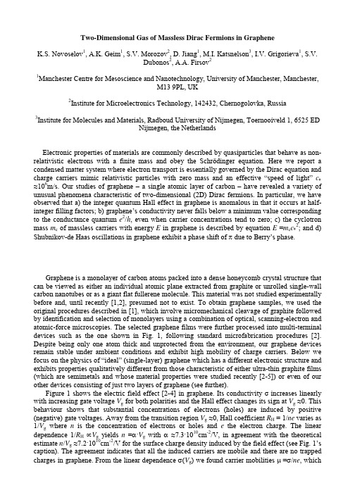
Two-Dimensional Gas of Massless Dirac Fermions in Graphene K.S. Novoselov1, A.K. Geim1, S.V. Morozov2, D. Jiang1, M.I. Katsnelson3, I.V. Grigorieva1, S.V. Dubonos2, A.A. Firsov21Manchester Centre for Mesoscience and Nanotechnology, University of Manchester, Manchester, M13 9PL, UK2Institute for Microelectronics Technology, 142432, Chernogolovka, Russia3Institute for Molecules and Materials, Radboud University of Nijmegen, Toernooiveld 1, 6525 ED Nijmegen, the NetherlandsElectronic properties of materials are commonly described by quasiparticles that behave as nonrelativistic electrons with a finite mass and obey the Schrödinger equation. Here we report a condensed matter system where electron transport is essentially governed by the Dirac equation and charge carriers mimic relativistic particles with zero mass and an effective “speed of light” c∗ ≈106m/s. Our studies of graphene – a single atomic layer of carbon – have revealed a variety of unusual phenomena characteristic of two-dimensional (2D) Dirac fermions. In particular, we have observed that a) the integer quantum Hall effect in graphene is anomalous in that it occurs at halfinteger filling factors; b) graphene’s conductivity never falls below a minimum value corresponding to the conductance quantum e2/h, even when carrier concentrations tend to zero; c) the cyclotron mass mc of massless carriers with energy E in graphene is described by equation E =mcc∗2; and d) Shubnikov-de Haas oscillations in graphene exhibit a phase shift of π due to Berry’s phase.Graphene is a monolayer of carbon atoms packed into a dense honeycomb crystal structure that can be viewed as either an individual atomic plane extracted from graphite or unrolled single-wall carbon nanotubes or as a giant flat fullerene molecule. This material was not studied experimentally before and, until recently [1,2], presumed not to exist. To obtain graphene samples, we used the original procedures described in [1], which involve micromechanical cleavage of graphite followed by identification and selection of monolayers using a combination of optical, scanning-electron and atomic-force microscopies. The selected graphene films were further processed into multi-terminal devices such as the one shown in Fig. 1, following standard microfabrication procedures [2]. Despite being only one atom thick and unprotected from the environment, our graphene devices remain stable under ambient conditions and exhibit high mobility of charge carriers. Below we focus on the physics of “ideal” (single-layer) graphene which has a different electronic structure and exhibits properties qualitatively different from those characteristic of either ultra-thin graphite films (which are semimetals and whose material properties were studied recently [2-5]) or even of our other devices consisting of just two layers of graphene (see further). Figure 1 shows the electric field effect [2-4] in graphene. Its conductivity σ increases linearly with increasing gate voltage Vg for both polarities and the Hall effect changes its sign at Vg ≈0. This behaviour shows that substantial concentrations of electrons (holes) are induced by positive (negative) gate voltages. Away from the transition region Vg ≈0, Hall coefficient RH = 1/ne varies as 1/Vg where n is the concentration of electrons or holes and e the electron charge. The linear dependence 1/RH ∝Vg yields n =α·Vg with α ≈7.3·1010cm-2/V, in agreement with the theoretical estimate n/Vg ≈7.2·1010cm-2/V for the surface charge density induced by the field effect (see Fig. 1’s caption). The agreement indicates that all the induced carriers are mobile and there are no trapped charges in graphene. From the linear dependence σ(Vg) we found carrier mobilities µ =σ/ne, whichreached up to 5,000 cm2/Vs for both electrons and holes, were independent of temperature T between 10 and 100K and probably still limited by defects in parent graphite. To characterise graphene further, we studied Shubnikov-de Haas oscillations (SdHO). Figure 2 shows examples of these oscillations for different magnetic fields B, gate voltages and temperatures. Unlike ultra-thin graphite [2], graphene exhibits only one set of SdHO for both electrons and holes. By using standard fan diagrams [2,3], we have determined the fundamental SdHO frequency BF for various Vg. The resulting dependence of BF as a function of n is plotted in Fig. 3a. Both carriers exhibit the same linear dependence BF = β·n with β ≈1.04·10-15 T·m2 (±2%). Theoretically, for any 2D system β is defined only by its degeneracy f so that BF =φ0n/f, where φ0 =4.14·10-15 T·m2 is the flux quantum. Comparison with the experiment yields f =4, in agreement with the double-spin and double-valley degeneracy expected for graphene [6,7] (cf. caption of Fig. 2). Note however an anomalous feature of SdHO in graphene, which is their phase. In contrast to conventional metals, graphene’s longitudinal resistance ρxx(B) exhibits maxima rather than minima at integer values of the Landau filling factor ν (Fig. 2a). Fig. 3b emphasizes this fact by comparing the phase of SdHO in graphene with that in a thin graphite film [2]. The origin of the “odd” phase is explained below. Another unusual feature of 2D transport in graphene clearly reveals itself in the T-dependence of SdHO (Fig. 2b). Indeed, with increasing T the oscillations at high Vg (high n) decay more rapidly. One can see that the last oscillation (Vg ≈100V) becomes practically invisible already at 80K whereas the first one (Vg <10V) clearly survives at 140K and, in fact, remains notable even at room temperature. To quantify this behaviour we measured the T-dependence of SdHO’s amplitude at various gate voltages and magnetic fields. The results could be fitted accurately (Fig. 3c) by the standard expression T/sinh(2π2kBTmc/heB), which yielded mc varying between ≈ 0.02 and 0.07m0 (m0 is the free electron mass). Changes in mc are well described by a square-root dependence mc ∝n1/2 (Fig. 3d). To explain the observed behaviour of mc, we refer to the semiclassical expressions BF = (h/2πe)S(E) and mc =(h2/2π)∂S(E)/∂E where S(E) =πk2 is the area in k-space of the orbits at the Fermi energy E(k) [8]. Combining these expressions with the experimentally-found dependences mc ∝n1/2 and BF =(h/4e)n it is straightforward to show that S must be proportional to E2 which yields E ∝k. Hence, the data in Fig. 3 unambiguously prove the linear dispersion E =hkc∗ for both electrons and holes with a common origin at E =0 [6,7]. Furthermore, the above equations also imply mc =E/c∗2 =(h2n/4πc∗2)1/2 and the best fit to our data yields c∗ ≈1⋅106 m/s, in agreement with band structure calculations [6,7]. The employed semiclassical model is fully justified by a recent theory for graphene [9], which shows that SdHO’s amplitude can indeed be described by the above expression T/sinh(2π2kBTmc/heB) with mc =E/c∗2. Note that, even though the linear spectrum of fermions in graphene (Fig. 3e) implies zero rest mass, their cyclotron mass is not zero. The unusual response of massless fermions to magnetic field is highlighted further by their behaviour in the high-field limit where SdHO evolve into the quantum Hall effect (QHE). Figure 4 shows Hall conductivity σxy of graphene plotted as a function of electron and hole concentrations in a constant field B. Pronounced QHE plateaux are clearly seen but, surprisingly, they do not occur in the expected sequence σxy =(4e2/h)N where N is integer. On the contrary, the plateaux correspond to half-integer ν so that the first plateau occurs at 2e2/h and the sequence is (4e2/h)(N + ½). Note that the transition from the lowest hole (ν =–½) to lowest electron (ν =+½) Landau level (LL) in graphene requires the same number of carriers (∆n =4B/φ0 ≈1.2·1012cm-2) as the transition between other nearest levels (cf. distances between minima in ρxx). This results in a ladder of equidistant steps in σxy which are not interrupted when passing through zero. To emphasize this highly unusual behaviour, Fig. 4 also shows σxy for a graphite film consisting of only two graphene layers where the sequence of plateaux returns to normal and the first plateau is at 4e2/h, as in the conventional QHE. We attribute this qualitative transition between graphene and its two-layer counterpart to the fact that fermions in the latter exhibit a finite mass near n ≈0 (as found experimentally; to be published elsewhere) and can no longer be described as massless Dirac particles. 2The half-integer QHE in graphene has recently been suggested by two theory groups [10,11], stimulated by our work on thin graphite films [2] but unaware of the present experiment. The effect is single-particle and intimately related to subtle properties of massless Dirac fermions, in particular, to the existence of both electron- and hole-like Landau states at exactly zero energy [912]. The latter can be viewed as a direct consequence of the Atiyah-Singer index theorem that plays an important role in quantum field theory and the theory of superstrings [13,14]. For the case of 2D massless Dirac fermions, the theorem guarantees the existence of Landau states at E=0 by relating the difference in the number of such states with opposite chiralities to the total flux through the system (note that magnetic field can also be inhomogeneous). To explain the half-integer QHE qualitatively, we invoke the formal expression [9-12] for the energy of massless relativistic fermions in quantized fields, EN =[2ehc∗2B(N +½ ±½)]1/2. In QED, sign ± describes two spins whereas in the case of graphene it refers to “pseudospins”. The latter have nothing to do with the real spin but are “built in” the Dirac-like spectrum of graphene, and their origin can be traced to the presence of two carbon sublattices. The above formula shows that the lowest LL (N =0) appears at E =0 (in agreement with the index theorem) and accommodates fermions with only one (minus) projection of the pseudospin. All other levels N ≥1 are occupied by fermions with both (±) pseudospins. This implies that for N =0 the degeneracy is half of that for any other N. Alternatively, one can say that all LL have the same “compound” degeneracy but zeroenergy LL is shared equally by electrons and holes. As a result the first Hall plateau occurs at half the normal filling and, oddly, both ν = –½ and +½ correspond to the same LL (N =0). All other levels have normal degeneracy 4B/φ0 and, therefore, remain shifted by the same ½ from the standard sequence. This explains the QHE at ν =N + ½ and, at the same time, the “odd” phase of SdHO (minima in ρxx correspond to plateaux in ρxy and, hence, occur at half-integer ν; see Figs. 2&3), in agreement with theory [9-12]. Note however that from another perspective the phase shift can be viewed as the direct manifestation of Berry’s phase acquired by Dirac fermions moving in magnetic field [15,16]. Finally, we return to zero-field behaviour and discuss another feature related to graphene’s relativistic-like spectrum. The spectrum implies vanishing concentrations of both carriers near the Dirac point E =0 (Fig. 3e), which suggests that low-T resistivity of the zero-gap semiconductor should diverge at Vg ≈0. However, neither of our devices showed such behaviour. On the contrary, in the transition region between holes and electrons graphene’s conductivity never falls below a well-defined value, practically independent of T between 4 and 100K. Fig. 1c plots values of the maximum resistivity ρmax(B =0) found in 15 different devices, which within an experimental error of ≈15% all exhibit ρmax ≈6.5kΩ, independent of their mobility that varies by a factor of 10. Given the quadruple degeneracy f, it is obvious to associate ρmax with h/fe2 =6.45kΩ where h/e2 is the resistance quantum. We emphasize that it is the resistivity (or conductivity) rather than resistance (or conductance), which is quantized in graphene (i.e., resistance R measured experimentally was not quantized but scaled in the usual manner as R =ρL/w with changing length L and width w of our devices). Thus, the effect is completely different from the conductance quantization observed previously in quantum transport experiments. However surprising, the minimum conductivity is an intrinsic property of electronic systems described by the Dirac equation [17-20]. It is due to the fact that, in the presence of disorder, localization effects in such systems are strongly suppressed and emerge only at exponentially large length scales. Assuming the absence of localization, the observed minimum conductivity can be explained qualitatively by invoking Mott’s argument [21] that mean-free-path l of charge carriers in a metal can never be shorter that their wavelength λF. Then, σ =neµ can be re-written as σ = (e2/h)kFl and, hence, σ cannot be smaller than ≈e2/h per each type of carriers. This argument is known to have failed for 2D systems with a parabolic spectrum where disorder leads to localization and eventually to insulating behaviour [17,18]. For the case of 2D Dirac fermions, no localization is expected [17-20] and, accordingly, Mott’s argument can be used. Although there is a broad theoretical consensus [18-23,10,11] that a 2D gas of Dirac fermions should exhibit a minimum 3conductivity of about e2/h, this quantization was not expected to be accurate and most theories suggest a value of ≈e2/πh, in disagreement with the experiment. In conclusion, graphene exhibits electronic properties distinctive for a 2D gas of particles described by the Dirac rather than Schrödinger equation. This 2D system is not only interesting in itself but also allows one to access – in a condensed matter experiment – the subtle and rich physics of quantum electrodynamics [24-27] and provides a bench-top setting for studies of phenomena relevant to cosmology and astrophysics [27,28].1. Novoselov, K.S. et al. PNAS 102, 10451 (2005). 2. Novoselov, K.S. et al. Science 306, 666 (2004); cond-mat/0505319. 3. Zhang, Y., Small, J.P., Amori, M.E.S. & Kim, P. Phys. Rev. Lett. 94, 176803 (2005). 4. Berger, C. et al. J. Phys. Chem. B, 108, 19912 (2004). 5. Bunch, J.S., Yaish, Y., Brink, M., Bolotin, K. & McEuen, P.L. Nanoletters 5, 287 (2005). 6. Dresselhaus, M.S. & Dresselhaus, G. Adv. Phys. 51, 1 (2002). 7. Brandt, N.B., Chudinov, S.M. & Ponomarev, Y.G. Semimetals 1: Graphite and Its Compounds (North-Holland, Amsterdam, 1988). 8. Vonsovsky, S.V. and Katsnelson, M.I. Quantum Solid State Physics (Springer, New York, 1989). 9. Gusynin, V.P. & Sharapov, S.G. Phys. Rev. B 71, 125124 (2005). 10. Gusynin, V.P. & Sharapov, S.G. cond-mat/0506575. 11. Peres, N.M.R., Guinea, F. & Castro Neto, A.H. cond-mat/0506709. 12. Zheng, Y. & Ando, T. Phys. Rev. B 65, 245420 (2002). 13. Kaku, M. Introduction to Superstrings (Springer, New York, 1988). 14. Nakahara, M. Geometry, Topology and Physics (IOP Publishing, Bristol, 1990). 15. Mikitik, G. P. & Sharlai, Yu.V. Phys. Rev. Lett. 82, 2147 (1999). 16. Luk’yanchuk, I.A. & Kopelevich, Y. Phys. Rev. Lett. 93, 166402 (2004). 17. Abrahams, E., Anderson, P.W., Licciardello, D.C. & Ramakrishnan, T.V. Phys. Rev. Lett. 42, 673 (1979). 18. Fradkin, E. Phys. Rev. B 33, 3263 (1986). 19. Lee, P.A. Phys. Rev. Lett. 71, 1887 (1993). 20. Ziegler, K. Phys. Rev. Lett. 80, 3113 (1998). 21. Mott, N.F. & Davis, E.A. Electron Processes in Non-Crystalline Materials (Clarendon Press, Oxford, 1979). 22. Morita, Y. & Hatsugai, Y. Phys. Rev. Lett. 79, 3728 (1997). 23. Nersesyan, A.A., Tsvelik, A.M. & Wenger, F. Phys. Rev. Lett. 72, 2628 (1997). 24. Rose, M.E. Relativistic Electron Theory (John Wiley, New York, 1961). 25. Berestetskii, V.B., Lifshitz, E.M. & Pitaevskii, L.P. Relativistic Quantum Theory (Pergamon Press, Oxford, 1971). 26. Lai, D. Rev. Mod. Phys. 73, 629 (2001). 27. Fradkin, E. Field Theories of Condensed Matter Systems (Westview Press, Oxford, 1997). 28. Volovik, G.E. The Universe in a Helium Droplet (Clarendon Press, Oxford, 2003).Acknowledgements This research was supported by the EPSRC (UK). We are most grateful to L. Glazman, V. Falko, S. Sharapov and A. Castro Netto for helpful discussions. K.S.N. was supported by Leverhulme Trust. S.V.M., S.V.D. and A.A.F. acknowledge support from the Russian Academy of Science and INTAS.43µ (m2/Vs)0.8c4P0.4 22 σ (1/kΩ)10K0 0 1/RH(T/kΩ) 1 2ρmax (h/4e2)1-5010 Vg (V) 50 -10ab 0 -100-500 Vg (V)50100Figure 1. Electric field effect in graphene. a, Scanning electron microscope image of one of our experimental devices (width of the central wire is 0.2µm). False colours are chosen to match real colours as seen in an optical microscope for larger areas of the same materials. Changes in graphene’s conductivity σ (main panel) and Hall coefficient RH (b) as a function of gate voltage Vg. σ and RH were measured in magnetic fields B =0 and 2T, respectively. The induced carrier concentrations n are described by [2] n/Vg =ε0ε/te where ε0 and ε are permittivities of free space and SiO2, respectively, and t ≈300 nm is the thickness of SiO2 on top of the Si wafer used as a substrate. RH = 1/ne is inverted to emphasize the linear dependence n ∝Vg. 1/RH diverges at small n because the Hall effect changes its sign around Vg =0 indicating a transition between electrons and holes. Note that the transition region (RH ≈ 0) was often shifted from zero Vg due to chemical doping [2] but annealing of our devices in vacuum normally allowed us to eliminate the shift. The extrapolation of the linear slopes σ(Vg) for electrons and holes results in their intersection at a value of σ indistinguishable from zero. c, Maximum values of resistivity ρ =1/σ (circles) exhibited by devices with different mobilites µ (left y-axis). The histogram (orange background) shows the number P of devices exhibiting ρmax within 10% intervals around the average value of ≈h/4e2. Several of the devices shown were made from 2 or 3 layers of graphene indicating that the quantized minimum conductivity is a robust effect and does not require “ideal” graphene.ρxx (kΩ)0.60 aVg = -60V4B (T)810K12∆σxx (1/kΩ)0.4 1ν=4 140K 80K B =12T0 b 0 25 50 Vg (V) 7520K100Figure 2. Quantum oscillations in graphene. SdHO at constant gate voltage Vg as a function of magnetic field B (a) and at constant B as a function of Vg (b). Because µ does not change much with Vg, the constant-B measurements (at a constant ωcτ =µB) were found more informative. Panel b illustrates that SdHO in graphene are more sensitive to T at high carrier concentrations. The ∆σxx-curves were obtained by subtracting a smooth (nearly linear) increase in σ with increasing Vg and are shifted for clarity. SdHO periodicity ∆Vg in a constant B is determined by the density of states at each Landau level (α∆Vg = fB/φ0) which for the observed periodicity of ≈15.8V at B =12T yields a quadruple degeneracy. Arrows in a indicate integer ν (e.g., ν =4 corresponds to 10.9T) as found from SdHO frequency BF ≈43.5T. Note the absence of any significant contribution of universal conductance fluctuations (see also Fig. 1) and weak localization magnetoresistance, which are normally intrinsic for 2D materials with so high resistivity.75 BF (T) 500.2 0.11/B (1/T)b5 10 N 1/2025 a 0 0.061dmc /m00.04∆0.02 0c0 0 T (K) 150n =0e-6-3036Figure 3. Dirac fermions of graphene. a, Dependence of BF on carrier concentration n (positive n correspond to electrons; negative to holes). b, Examples of fan diagrams used in our analysis [2] to find BF. N is the number associated with different minima of oscillations. Lower and upper curves are for graphene (sample of Fig. 2a) and a 5-nm-thick film of graphite with a similar value of BF, respectively. Note that the curves extrapolate to different origins; namely, to N = ½ and 0. In graphene, curves for all n extrapolate to N = ½ (cf. [2]). This indicates a phase shift of π with respect to the conventional Landau quantization in metals. The shift is due to Berry’s phase [9,15]. c, Examples of the behaviour of SdHO amplitude ∆ (symbols) as a function of T for mc ≈0.069 and 0.023m0; solid curves are best fits. d, Cyclotron mass mc of electrons and holes as a function of their concentration. Symbols are experimental data, solid curves the best fit to theory. e, Electronic spectrum of graphene, as inferred experimentally and in agreement with theory. This is the spectrum of a zero-gap 2D semiconductor that describes massless Dirac fermions with c∗ 300 times less than the speed of light.n (1012 cm-2)σxy (4e2/h)4 3 2 -2 1 -1 -2 -3 2 44Kn7/ 5/ 3/ 1/2 2 2 210 ρxx (kΩ)-4σxy (4e2/h)0-1/2 -3/2 -5/2514T0-7/2 -4 -2 0 2 4 n (1012 cm-2)Figure 4. Quantum Hall effect for massless Dirac fermions. Hall conductivity σxy and longitudinal resistivity ρxx of graphene as a function of their concentration at B =14T. σxy =(4e2/h)ν is calculated from the measured dependences of ρxy(Vg) and ρxx(Vg) as σxy = ρxy/(ρxy + ρxx)2. The behaviour of 1/ρxy is similar but exhibits a discontinuity at Vg ≈0, which is avoided by plotting σxy. Inset: σxy in “two-layer graphene” where the quantization sequence is normal and occurs at integer ν. The latter shows that the half-integer QHE is exclusive to “ideal” graphene.。

CHEMICAL INDUSTRY AND ENGINEERING PROGRESS 2017年第36卷第2期·602·化 工 进 展石墨烯基复合材料去除水中重金属研究进展滕洪辉,彭雪,高彬(吉林师范大学环境科学与工程学院,吉林 四平136000)摘要:近几年,石墨烯及其复合材料因其比表面积大、传输电子能力强、结构稳定、可吸附多种污染物,被认为是极具发展潜力的环保新材料,尤其是在重金属分离方面具有明显的优势。
本文综述了各类石墨烯材料在水中重金属去除方面的研究现状,对比分析了不同材料对镉、汞、铬、铜、铅、锌和砷离子的去除能力及机理。
认为石墨烯复合材料在水中分散情况、活性官能团种类、电子传输能力调控和重复使用性能对重金属离子去除有重要影响。
指出控制石墨烯片层聚集、增加亲水性、提高可回收性和制备高灵敏选择性电极将是石墨烯材料修饰改性的研究热点。
此外,石墨烯复合材料对一些有机污染物也有良好的吸附能力,制备能够吸附多类别污染物的净水剂也将成为石墨烯复合材料的一个主要研究方向。
关键词:石墨烯;复合材料;吸附中图分类号:X703 文献标志码:A 文章编号:1000–6613(2017)02–0602–09 DOI :10.16085/j.issn.1000-6613.2017.02.028Removal of heavy metals from water by graphene compositesTENG Honghui ,PENG Xue ,GAO Bin(College of Environmental Science and Engineering ,Jilin Normal University ,Siping 136000,Jilin ,China )Abstract :In recent years ,graphene and its composites are considered new promising environmentalprotection materials ,because they have large specific surface area ,strong transmission electron ability and stable structure which renders them ability to adsorb more kinds of pollutants than other materials ,especially for heavy metals. The current researches of the removal of heavy metals from the water by graphene materials are reviewed in this paper. The removal ability and mechanism of cadmium ,mercury ,chromium ,copper ,lead ,zinc and arsenic ions by graphene materials are analyzed. The results show that the dispersion of graphene materials in water ,the type of reactive functional groups ,control of electronic transmission and the reuse performance of graphene composites have significant effects on the removal of heavy metal ions. We also point out that controlling graphene layers aggregation ,increasing the hydrophilicity ,improving the recycle ability and preparing high sensitive selective electrode will be hot topics of graphene materials modified researches. In addition ,graphene composites also have good adsorption capacity for some organic pollutants ,so the preparation of graphene composites as purifiers for many pollutants will become one of the main research directions of graphene composites.Key words :graphene ;composites ;adsorption水环境中存在的大量重金属严重影响了动植物的正常生长,对生态系统和人类健康构成了极大的威胁。
第 22卷第 3期2023年 3月Vol.22 No.3Mar.2023软件导刊Software Guide融合注意力机制的知识图谱推荐模型李君,倪晓军(南京邮电大学计算机学院、软件学院、网络空间安全学院,江苏南京 210000)摘要:知识图谱在推荐领域得到了广泛关注,通常被用来作为辅助信息嵌入到推荐模型中,以更好地缓解传统推荐算法数据稀疏和冷启动问题。
但是部分模型的输入向量较为稀疏,也没有充分挖掘用户与物品之间的特征交互,进而影响模型性能。
因此,提出一种基于 FGCNN 与 MKR 的融合注意力机制的知识图谱推荐模型(BAKR)。
首先,利用 FGCNN 的 Feature Generation 模块提取用户和物品的特征向量;其次,使用知识图谱获取实体之间的依赖关系,将隐含的辅助信息嵌入到模型中,再通过注意力机制重新分配用户的偏好权重值,进而更好地协助推荐任务,提高推荐性能;最后,在 MovieLens-1M 数据集和Book-Crossing数据集上进行仿真实验。
结果证明,该模型可显著提升推荐的准确率。
关键词:推荐模型;知识图谱;注意力机制DOI:10.11907/rjdk.222429开放科学(资源服务)标识码(OSID):中图分类号:TP391.3 文献标识码:A文章编号:1672-7800(2023)003-0118-07Knowledge Graph Recommendation Model Integrating Attention MechanismLI Jun, NI Xiao-jun(School of Computer Science, Nanjing University of Posts and Telecommunications, Nanjing 210000, China)Abstract:Knowledge graph has received extensive attention in the field of recommendation, and it is often used as auxiliary information to be embedded in recommendation models to better alleviate the data sparsity and cold start problems of traditional recommendation algorithms. However, the input vector of some models is relatively sparse, and the feature interaction between users and items is not fully explored, which makes the representation between users and items less accurate and affects the performance of the model. Therefore, a knowledge graph recom⁃mendation model (BAKR) based on the fusion attention mechanism of FGCNN and MKR is proposed. First, FGCNN′s Feature Generation module is used to extract feature vectors of users and items. Secondly, the knowledge graph is used to obtain the dependencies between enti⁃ties, embed the implied auxiliary information into the model, and then redistribute the user′s preference weight value through the attention mechanism to better assist the recommendation task and improve the recommendation performance. Finally, simulation experiments are car⁃ried out on the MovieLens-1M and Book-Crossing dataset, and the experimental results show that the accuracy of the model for the recommen⁃dation effect is significantly improved.Key Words:recommendation system; knowledge graph; attention mechanism0 引言随着信息化社会的发展,其产生的数据量进一步爆炸式增长[1],人们所面临的问题不再是信息匮乏,而是如何从海量数据中获取用户需要的信息(如商品、电影、书籍等)。
中考化学材料英语阅读理解25题1<背景文章>In recent years, there has been a growing interest in new eco-friendly materials. One such material is a biodegradable plastic that is made from renewable resources. This plastic has several remarkable characteristics.It is strong and durable, yet it can break down naturally over time. This makes it an ideal choice for packaging materials, as it reduces the amount of waste that ends up in landfills. Moreover, it is lightweight, which lowers transportation costs.Another advantage of this material is its versatility. It can be used in a wide range of applications, from food packaging to construction materials. For example, it can be molded into different shapes and sizes for packaging various products. In the construction industry, it can be used to make insulation panels that are energy-efficient.The development of eco-friendly materials like this biodegradable plastic is crucial for a sustainable future. As the world becomes more aware of the environmental impact of traditional materials, the demand for sustainable alternatives is on the rise.1. What is one of the characteristics of the biodegradable plastic?A. Weak and fragile.B. Strong and durable.C. Heavy and bulky.D. Expensive and rare.答案:B。
上海科学院研究所开展外向型业务途径探索
方正;戴燕玲
【期刊名称】《科技管理咨询》
【年(卷),期】1990(000)004
【总页数】2页(P24-25)
【作者】方正;戴燕玲
【作者单位】不详;不详
【正文语种】中文
【中图分类】G311
【相关文献】
1.广西社会科学院东南亚研究所和上海社会科学院亚洲太平洋研究所共同举办"国际格局变化中的亚太与东南亚"学术讨论会 [J], 雷小华
2.我国著各有机化学家中国科学院上海有机化学研究所研究员中国科学院院士 [J], 无;
3.疾风劲草红外筑梦——记中国科学院院士、中国科学院上海技术物理研究所研究员褚君浩 [J], 段盼盼; 吴彪
4.赤子传——记中国科学院院士、中国科学院上海技术物理研究所研究员褚君浩[J], 吴彪[1]
5.螯合白血病患者骨髓细胞内外钙离子对硫化氢生成影响的实验研究相关检索词免疫组化蛋白表达白血病硫化细胞增殖 cell proliferation bax h2s 骨髓胃癌硫化氢细胞周期 bcl-2 间充质干细胞图像分析单个核细胞电极乳腺癌钙离子leukemia 相关专家李杰张旻李艳平葛楚天相关机构· 中国科学院上海生命科学研究院生物化学与细胞生物学研究所· 中国科学院上海生命科学研究院· 北京师范
大学· 浙江大学动物科学学院· 浙江大学螯合白血病患者骨髓细胞内外钙离子对硫化氢生成影响的实验研究 [J], 孙晓红;于志刚;张雪莉;庄宝祥;张圣明
因版权原因,仅展示原文概要,查看原文内容请购买。
Ultra-High Efficiency Photovoltaic Cells for Large Scale Solar Power GenerationYoshiaki NakanoAbstract The primary targets of our project are to dras-tically improve the photovoltaic conversion efficiency and to develop new energy storage and delivery technologies. Our approach to obtain an efficiency over40%starts from the improvement of III–V multi-junction solar cells by introducing a novel material for each cell realizing an ideal combination of bandgaps and lattice-matching.Further improvement incorporates quantum structures such as stacked quantum wells and quantum dots,which allow higher degree of freedom in the design of the bandgap and the lattice strain.Highly controlled arrangement of either quantum dots or quantum wells permits the coupling of the wavefunctions,and thus forms intermediate bands in the bandgap of a host material,which allows multiple photon absorption theoretically leading to a conversion efficiency exceeding50%.In addition to such improvements, microfabrication technology for the integrated high-effi-ciency cells and the development of novel material systems that realizes high efficiency and low cost at the same time are investigated.Keywords Multi-junctionÁQuantum wellÁConcentratorÁPhotovoltaicINTRODUCTIONLarge-scale photovoltaic(PV)power generation systems, that achieve an ultra-high efficiency of40%or higher under high concentration,are in the spotlight as a new technology to ease drastically the energy problems.Mul-tiple junction(or tandem)solar cells that use epitaxial crystals of III–V compound semiconductors take on the active role for photoelectric energy conversion in such PV power generation systems.Because these solar cells operate under a sunlight concentration of5009to10009, the cost of cells that use the epitaxial crystal does not pose much of a problem.In concentrator PV,the increased cost for a cell is compensated by less costly focusing optics. The photons shining down on earth from the sun have a wide range of energy distribution,from the visible region to the infrared region,as shown in Fig.1.Multi-junction solar cells,which are laminated with multilayers of p–n junctions configured by using materials with different band gaps,show promise in absorbing as much of these photons as possible,and converting the photon energy into elec-tricity with minimum loss to obtain high voltage.Among the various types of multi-junction solar cells,indium gallium phosphide(InGaP)/gallium arsenide(GaAs)/ger-manium(Ge)triple-junction cells that make full use of the relationship between band gaps and diverse lattice con-stants offered by compound semiconductors have the advantage of high conversion efficiency because of their high-quality single crystal with a uniform-size crystal lat-tice.So far,a conversion efficiency exceeding41%under conditions where sunlight is concentrated to an intensity of approximately5009has been reported.The tunnel junction with a function equivalent to elec-trodes is inserted between different materials.The positive holes accumulated in the p layer and the electrons in the adjacent n layer will be recombined and eliminated in the tunnel junction.Therefore,three p–n junctions consisting of InGaP,GaAs,and Ge will become connected in series. The upper limit of the electric current is set by the mini-mum value of photonflux absorbed by a single cell.On the other hand,the sum of voltages of three cells make up the voltage.As shown in Fig.1,photons that can be captured in the GaAs middle cell have a smallflux because of the band gap of each material.As a result,the electric currentoutputAMBIO2012,41(Supplement2):125–131 DOI10.1007/s13280-012-0267-4from the GaAs cell theoretically becomes smaller than that of the others and determines the electric current output of the entire tandem cell.To develop a higher efficiency tandem cell,it is necessary to use a material with a band gap narrower than that of GaAs for the middle cell.In order to obtain maximum conversion efficiency for triple-junction solar cells,it is essential to narrow down the middle cell band gap to 1.2eV and increase the short-circuit current density by 2mA/cm 2compared with that of the GaAs middle cell.When the material is replaced with a narrower band gap,the output voltage will drop.However,the effect of improving the electric current balance out-performs this drop in output voltage and boosts the effi-ciency of the entire multi-junction cell.When a crystal with such a narrow band gap is grown on a Ge base material,lattice relaxation will occur in the middle of epitaxial crystal growth because the lattice constants of narrower band-gap materials are larger than that of Ge (as shown in Fig.2).As a result,the carrier transport properties will degrade due to dislocation.Researchers from the international research center Solar Quest,the University of Tokyo,aim to move beyond such material-related restrictions,and obtain materials and structures that have effective narrow band gaps while maintaining lattice matching with Ge or GaAs.To achieve this goal,we have taken three approaches as indicated in Fig.3.These approaches are explained in detail below.DILUTE NITROGEN-ADDED BULK CRYSTAL Indium gallium nitride arsenide (InGaNAs)is a bulk material consists of InGaAs,which contains several percent of nitrogen.InGaNAs has a high potential for achieving a narrow band gap while maintaining lattice matching with Ge or GaAs.However,InGaNAs has a fatal problem,that is,a drop in carrier mobility due to inhomogeneousdistribution of nitrogen (N).To achieve homogeneous solid solution of N in crystal,we have applied atomic hydrogen irradiation in the film formation process and addition of a very small amount of antimony (Sb)(Fig.3).The atomic hydrogen irradiation technology and the nitrogen radical irradiation technology for incorporating N efficiently into the crystal can be achieved only through molecular beam epitaxy (MBE),which is used to fabricate films under high vacuum conditions.(Nitrogen radical irradiation is a technology that irradiates the surface of a growing crystal with nitrogen atoms that are resolved by passing nitrogen through a plasma device attached to the MBE system.)Therefore,high-quality InGaNAs has been obtained only by MBE until now.Furthermore,as a small amount of Sb is also incorporated in a crystal,it is nec-essary to control the composition of five elements in the crystal with a high degree of accuracy to achieve lattice matching with Ge or GaAs.We have overcome this difficulty by optimizing the crystal growth conditions with high precision and devel-oped a cell that has an InGaNAs absorption layer formed on a GaAs substrate.The short-circuit current has increased by 9.6mA/cm 2for this cell,compared with a GaAs single-junction cell,by narrowing the band gap down to 1.0eV.This technology can be implemented not only for triple-junction cells,but also for higher efficiency lattice-matched quadruple-junction cells on a Ge substrate.In order to avoid the difficulty of adjusting the compo-sition of five elements in a crystal,we are also taking an approach of using GaNAs with a lattice smaller than that of Ge or GaAs for the absorption layer and inserting InAs with a large lattice in dot form to compensate for the crystal’s tensile strain.To make a solid solution of N uniformly in GaNAs,we use the MBE method for crystal growth and the atomic hydrogen irradiation as in the case of InGaNAs.We also believe that using 3D-shaped InAs dots can effectively compensate for the tensile strainthatFig.1Solar spectrum radiated on earth and photon flux collected by the top cell (InGaP),middle cell (GaAs),and bottom cell (Ge)(equivalent to the area of the filled portions in the figure)occurs in GaNAs.We have measured the characteristics of a single-junction cell formed on a GaAs substrate by using a GaNAs absorption layer with InAs dots inserted.Figure 4shows that we were able to succeed in enhancing the external quantum efficiency in the long-wavelength region (corresponding to the GaNAs absorp-tion)to a level equal to GaAs.This was done by extending the absorption edge to a longer wavelength of 1200nm,and increasing the thickness of the GaNAs layer by increasing the number of laminated InAs quantum dot layers.This high quantum efficiency clearly indicates that GaNAs with InAs dots inserted has the satisfactory quality for middle cell material (Oshima et al.2010).STRAIN-COMPENSATED QUANTUM WELL STRUCTUREIt is extremely difficult to develop a narrow band-gap material that can maintain lattice matching with Ge orGaAs unless dilute nitrogen-based materials mentioned earlier are used.As shown in Fig.2,the conventionally used material InGaAs has a narrower band gap and a larger lattice constant than GaAs.Therefore,it is difficult to grow InGaAs with a thickness larger than the critical film thickness on GaAs without causing lattice relaxation.However,the total film thickness of InGaAs can be increased as an InGaAs/GaAsP strain-compensated multi-layer structure by laminating InGaAs with a thickness less than the critical film thickness in combination with GaAsP that is based on GaAs as well,but has a small lattice constant,and bringing the average strain close to zero (Fig.3.).This InGaAs/GaAsP strain-compensated multilayer structure will form a quantum well-type potential as shown in Fig.5.The narrow band-gap InGaAs layer absorbs the long-wavelength photons to generate electron–hole pairs.When these electron–hole pairs go over the potential bar-rier of the GaAsP layer due to thermal excitation,the electrons and holes are separated by a built-in electricfieldFig.2Relationship between band gaps and lattice constants of III–V-based and IV-based crystalsto generate photocurrent.There is a high probability of recombination of electron–hole pairs that remain in the well.To avoid this recombination,it is necessary to take out the electron–hole pairs efficiently from the well and transfer them to n-type and p-type regions without allowing them to be recaptured into the well.Designing thequantumFig.3Materials and structures of narrow band-gap middle cells being researched by thisteamFig.4Spectral quantum efficiency of GaAs single-junction cell using GaNAs bulk crystal layer (inserted with InAs dots)as the absorption layer:Since the InAs dot layer and the GaNAs bulk layer are stacked alternately,the total thickness of GaNAs layers increases as the number of stacked InAs dot layers is increased.The solid line in the graph indicates the data of a reference cell that uses GaAs for its absorption layer (Oshima et al.2010)well structure suited for this purpose is essential for improving conversion efficiency.The high-quality crystal growth by means of the metal-organic vapor phase epitaxy (MOVPE)method with excellent ability for mass production has already been applied for InGaAs and GaAsP layers in semiconductor optical device applications.Therefore,it is technologically quite possible to incorporate the InGaAs/GaAsP quantum well structure into multi-junction solar cells that are man-ufactured at present,only if highly accurate strain com-pensation can be achieved.As the most basic approach related to quantum well structure design,we are working on fabrication of super-lattice cells with the aim of achieving higher efficiency by making the GaAsP barrier layer as thin as possible,and enabling carriers to move among wells by means of the tunnel effect.Figure 6shows the spectral quantum effi-ciency of a superlattice cell.In this example,the thickness of the GaAsP barrier layer is 5nm,which is not thin enough for proper demonstration of the tunnel effect.When the quantum efficiency in the wavelength range (860–960nm)that corresponds to absorption of the quan-tum well is compared between a cell,which has a con-ventionally used barrier layer and a thickness of 10nm or more,and a superlattice cell,which has the same total layer thickness of InGaAs,the superlattice cell demonstrates double or higher quantum efficiency.This result indicates that carrier mobility across quantum wells is promoted by even the partial use of the tunnel effect.By increasing the P composition in the GaAsP layer,the thickness of well (or the In composition)can be increased,and the barrier layer thickness can be reduced while strain compensation is maintained.A cell with higher quantum efficiency can befabricated while extending the absorption edge to the long-wavelength side (Wang et al.2010,2012).GROWTH TECHNIQUE FOR STRAIN-COMPENSATED QUANTUM WELLTo reduce the strain accumulated in the InGaAs/GaAsP multilayer structure as close to zero as possible,it is nec-essary to control the thickness and atomic content of each layer with high accuracy.The In composition and thickness of the InGaAs layer has a direct effect on the absorption edge wavelength and the GaAsP layer must be thinned to a satisfactory extent to demonstrate fully the tunnel effect of the barrier layer.Therefore,it is desirable that the average strain of the entire structure is adjusted mainly by the P composition of the GaAsP layer.Meanwhile,for MOVPE,there exists a nonlinear rela-tionship between the P composition of the crystal layer and the P ratio [P/(P ?As)]in the vapor phase precursors,which arises from different absorption and desorption phenomena on the surface.As a result,it is not easy to control the P composition of the crystal layer.To break through such a difficulty and promote efficient optimiza-tion of crystal growth conditions,we have applied a mechanism to evaluate the strain of the crystal layer during growth in real time by sequentially measuring the curvature of wafers during growth with an incident laser beam from the observation window of the reactor.As shown in Fig.7,the wafer curvature during the growth of an InGaAs/GaAsP multilayer structure indicates a periodic behavior.Based on a simple mechanical model,it has become clear that the time changes ofwaferFig.5Distribution of potential formed by the InGaAs/GaAsP strain-compensated multilayer structure:the narrow band-gap InGaAs layer is sandwiched between wide band-gap GaAsP layers and,as a result,it as quantum well-type potential distribution.In the well,electron–hole pairs are formed by absorption of long-wavelength photons and at the same time,recombination of electrons and holes takes place.The team from Solar Quest is focusing on developing a superlattice structure with the thinnest GaAsP barrier layercurvature are proportionate to the strain of the crystal layer relative to a substrate during the growing process.One vibration cycle of the curvature is same as the growth time of an InGaAs and GaAsP pair (Sugiyama et al.2011).Therefore,the observed vibration of the wafer curvature reflects the accumulation of the compression strain that occurs during InGaAs growth and the release of the strain that occurs during GaAsP growth.When the strain is completely compensated,the growth of the InGaAs/GaAsP pair will cause this strain to return to the initial value and the wafer curvature will vibrate with the horizontal line as the center.As shown in Fig.7,strain can be compensated almost completely by adjusting the layer structure.Only by conducting a limited number of test runs,the use of such real-time observation technology of the growth layer enables setting the growth conditions for fabricating the layer structure for which strain has been compensated with highaccuracy.Fig.6Spectral quantum efficiency of GaAs single-junction cell using InGaAs/GaAsP superlattice as theabsorption layer:This structure consists of 60layers of InGaAs quantum wells.The graph also shows data of a reference cell that uses GaAs for its absorption layer (Wang et al.2010,2012)Fig.7Changes in wafer curvature over time during growth of the InGaAs/GaAsP multilayer structure.This graph indicates the measurement result and the simulation result of the curvature based on the layer structure(composition ?thickness)obtained by X-ray diffraction.Since compressive strain is applied during InGaAs growth,the curvature decreases as time passes.On the other hand,since tensile strain is applied during GaAsP growth,the curvature changes in the oppositedirection (Sugiyama et al.2011)FUTURE DIRECTIONSIn order to improve the conversion efficiency by enhancing the current matching of multi-junction solar cells using III–V compound semiconductors,there is an urgent need to create semiconductor materials or structures that can maintain lattice matching with Ge or GaAs,and have a band gap of1.2eV.As for InGaNAs,which consists of InGaAs with several percent of nitrogen added,we have the prospect of extending the band edge to1.0eV while retaining sufficient carrier mobility for solar cells by means of atomic hydrogen irradiation and application of a small quantity of Sb during the growth process.In addition,as for GaNAs bulk crystal containing InAs dots,we were able to extend the band edge to1.2eV and produce a high-quality crystal with enoughfilm thickness to achieve the quantum efficiency equivalent to that of GaAs.These crystals are grown by means of MBE. Therefore,measures that can be used to apply these crys-tals for mass production,such as migration to MOVPE, will be investigated after demonstrating their high effi-ciency by embedding these crystals into multi-junction cells.As for the InGaAs/GaAsP strain-compensated quantum well that can be grown using MOVPE,we are working on the development of a thinner barrier layer while compen-sating for the strain with high accuracy by real-time observation of the wafer curvature.We have had the prospect of achieving a quantum efficiency that will sur-pass existing quantum well solar cells by promoting the carrier transfer within the multilayer quantum well struc-ture using the tunnel effect.As this technology can be transferred quite easily to the existing multi-junction solar cell fabrication process,we strongly believe that this technology can significantly contribute to the efficiency improvement of the latest multi-junction solar cells. REFERENCESOshima,R.,A.Takata,Y.Shoji,K.Akahane,and Y.Okada.2010.InAs/GaNAs strain-compensated quantum dots stacked up to50 layers for use in high-efficiency solar cell.Physica E42: 2757–2760.Sugiyama,M.,K.Sugita,Y.Wang,and Y.Nakano.2011.In situ curvature monitoring for metalorganic vapor phase epitaxy of strain-balanced stacks of InGaAs/GaAsP multiple quantum wells.Journal of Crystal Growth315:1–4.Wang,Y.,Y.Wen,K.Watanabe,M.Sugiyama,and Y.Nakano.2010.InGaAs/GaAsP strain-compensated superlattice solar cell for enhanced spectral response.In Proceedings35th IEEE photovoltaic specialists conference,3383–3385.Wang,Y.P.,S.Ma,M.Sugiyama,and Y.Nakano.2012.Management of highly-strained heterointerface in InGaAs/GaAsP strain-balanced superlattice for photovoltaic application.Journal of Crystal Growth.doi:10.1016/j.jcrysgro.2011.12.049. AUTHOR BIOGRAPHYYoshiaki Nakano(&)is Professor and Director General of Research Center for Advanced Science and Technology,the University of Tokyo.His research interests include physics and fabrication tech-nologies of semiconductor distributed feedback lasers,semiconductor optical modulators/switches,monolithically integrated photonic cir-cuits,and high-efficiency heterostructure solar cells.Address:Research Center for Advanced Science and Technology, The University of Tokyo,4-6-1Komaba,Meguro-ku,Tokyo153-8904,Japan.e-mail:nakano@rcast.u-tokyo.ac.jp。
A multi-layer graphene diaphragm based fiber-optic Fabry-Perot foracoustic measurementJun Ma and Wei JinDepartment of Electrical Engineering, The Hong Kong Polytechnic University, Hong Kong, Chinaeejun.ma@connect.polyu.hkABSTRACTA fiber-optic Fabry-Perot pressure sensor with a ~100 nm-thick multi-layer graphene diaphragm is fabricated. Static pressure test demonstrates a pressure-induced diaphragm deflection of over 625 nm/kPa, while dynamic (acoustic) pressure test shows a pressure-induced deflection of 1100 nm/kPa. The sensor exhibits a noise equivalent acoustic signal level of ~ 60 μPa/Hz1/2 at 10kHz and a flat frequency response from 0.2 to 22 kHz.Keywords: optical fiber sensor, graphene diaphragm, Fabry-Perot interferometer, acoustic sensor1. INTRODUCTIONFiber optic interferometers have been studied extensively for pressure and acoustic measurements because of a number of advantages such as high sensitivity, electromagnetic immunity, and remote detection and multiplexing capability [1]. Compared with Mach-Zehnder and Michelson interferometers, fiber-tip Fabry-Perot interferometers (FPI) formed between a cleaved fiber end and a reflective diaphragm have demonstrated high sensitivity without the need for a long length of optical fiber [2]. The smaller size of the fiber-tip FPIs make them especially attractive for space limited applications. FPI pressure/acoustic sensors with different diaphragm materials have been studied and the pressure sensitivity has been significantly improved by using thinner diaphragms with a reasonable size (or diameter) [2-6]. Recently, graphene as a single atomic layer of carbon has drawn significant attention due to its unique properties such as ultra-small thickness (0.335 nm) and high mechanic strength [7]. By use of a few-layer graphene film as deflectable diaphragm, we built a fiber-tip FPI and demonstrated a pressure sensitivity of 39.2 nm/kPa with a diaphragm of only 25 μm in diameter [8]. Increasing the diameter of the diaphragm could further improve the pressure sensitivity, however we found it is difficult to prepare and transfer larger-diameter graphene films with nanometer thickness to the fiber-tip.In this paper, we report a fiber-tip FPI made with a 125 μm-diameter multi-layer graphene diaphragm with a thickness of ~100 nm. Static and acoustic pressure tests show that the diaphragm has a pressure sensitivity (pressure-induced diaphragm deflection) from 625 to 1100 nm/kPa, and the sensor can detect acoustic signal as small as ~60 μPa/Hz1/2 at 10 kHz with a relatively uniform frequency response from 0.2 to 22 kHz.2. SENSOR FABRICATIONFig. 1(a) is the schematic of the sensor head that comprises of a zirconia ferrule, a standard single mode fiber (SMF), and a multi-layer graphene diaphragm. The SMF is cleaved and inser ted into the ferrule (inner diameter 125 μm), and the separation between the fiber end and the ferrule endface is controlled by use of a high resolution translation stage. The ferrule and the SMF are held together by the curable gel. The graphene diaphragm is prepared from the commercial graphene/Nickel(Ni)/graphene sample () in which the graphene film with an average thickness of 100 nm was grown by chemical vapor deposition (CVD) on a 25 μm-thick Ni foil. The process for separating the graphene diaphragm from the Ni foil and transferring it to the ferrule endface is similar to that in [8], the difference is that the graphene film on one side of the graphene/Ni/graphene sample was polished off before it was put into the ferric chloride (FeCl3) solution to etch the Ni foil off. Fig. 1(b) shows a photograph of the FPI sensor head. Figs. 1(c) and 1(d) show respectively the microscope images of the ferrule endface before and after it is covered with the graphene diaphragm. The graphene diaphragm is stuck to the ferrule endface by the van der Waals interaction [9, 10].(d)(c)SMFFerruleDiaphragm (a)(b)125 μm125 μmFig. 1. (a) Schematic of the FPI configuration: a 125 μm -diameter zirconia ferrule with a single mode fiber inserted into it and a graphene diaphragm covering its endface; (b) photograph of the fabricated FPI; microscope images of the ferrule endface (c) before and (d) after it is covered with the graphene diaphragm .The reflective surfaces at the cleaved fiber end and the graphene diaphragm form a low-finesse FPI, and the deflection of the diaphragm can be determined by interrogating the FPI in a reflection mode as described in [11]. Fig. 2 shows a typical reflection spectrum measured by use of a broadband source (BBS) in combination with an optical spectrum analyzer (OSA) with a 0.01 nm resolution. The cavity length, i.e., the separation between the fiber end and diaphragm, L can then be calculated from the measured spectrum by L=λ1λ2/2(λ1-λ2), where λ1 and λ2 are the adjacent peak/dip wavelengths of the interference spectrum.15401545155015551560-24-22-20-18-16-14-12-10R e l a t v i e i n t e n s i t y (d B )Wavelength (nm)Fig. 2. Interference spectrum of multi-layer graphene diaphragm based FPI.3. ACOUSTIC MESUREMENTTo demonstrate the potential of the FPI as a highly sensitive acoustic pressure sensor, we carry out test by using the experimental setup shown in Fig. 3. The acoustic signal is generated by the speaker driven by a signal generator. The FPI and the calibrated microphone (B&K4189) are positioned at two symmetry points to the central axis of the speaker. The wavelength of the tunable laser is tuned to the quadrature (Q) point of an interference fringe to maximize the acoustic sensitivity [15]. The reflected light of the FPI through an optical circulator is detected by the photo-detector (PD), while the electrical signal from the calibrated microphone goes through a conditioning amplifier. The electrical outputs from the PD and conditioning amplifier are received by either an real-time electrical spectrum analyzer or a lock-in amplifier. During the acoustic pressure test, the FPI, the calibration microphone and the speaker are put inside an acoustic isolation box.Tunable laser123Lock-in amplifierCirculator Conditioning amplifierFPI SpeakerSignal generatorPhoto-detectorAcoustic isolation boxB&K 418910 mV/Pa 26 uV/Pa7.50 mV 6.00 kHzReferenceFig. 3. Schematic of experimental setup for acoustic pressure measurement.Fig. 4(a) shows the output voltage signal of the FPI detected by the lock-in amplifier under different acoustic pressure levels at frequency of 10 kHz. The lock-in amplifier is set to 100 ms time constant with 18 dB/octave roll off . The acoustic pressure sensitivity of the FPI is estimated to be 13.15 mV/Pa. Under the approximation of two-beam interference, the output voltage V ac and the applied acoustic pressure may be related by [15],L S I V ac ∆⋅⋅⋅ℜ=max 0 (1)where, ℜ is the responsibility of the PD, I 0 is the light power of the laser at the Q-point , andλπnR R dL )(I/I d S 04221max ⋅==(2) is the slope of the normalized intensity change to the diaphragm deflection. R 1 and R 2 are respectively the reflectivities ofthe fiber end/air interface and the graphene diaphragm. By fitting the measured interference spectrum in Fig. 2, the maximum slope S max is estimated to be 0.16×10⁻³/nm, which is slightly higher than the theoretical value of 0.15×10⁻³/nm. In our experiment, I 0 =0.8 mW and ℜ=105 V/W. The diaphragm deflection of the FPI is calculated to be 1.1 nm/Pa by use of Eq. (1). Fig. 4(b) shows the frequency response of the FPI from 0.2 to 22 kHz, which is relatively uniform over this frequency range. The acoustic pressures generated form the speaker at different frequencies are calibrated by the microphone. The small ripples observed might be due to the interference of the incident acoustic wave and the acoustic waves reflected by the FPI and the microphone [6].1002003004000123456FPI outputLinear fit of FPI outputO u t p u t v o l t a g e s i g n a l (m V )Pressure Applied (mPa)Y=0.01315*X-0.00004(a)(b)51015200.010.11101001000S e n s i t i v i t y (m V /P a )Frequency (kHz)Fig. 4. (a) Output voltage signal of the FPI for varying applied acoustic pressure levels at the frequency of 10 kHz; (b) frequency response of the FPI.Fig. 5(a) shows the power spectrum of the FPI output measured with the real-time electrical spectrum analyzer when an acoustic pressure of 400 mPa was applied at 10 kHz. The noise floor is about -91 dBm with a 50 Hz bandwidth. For the acoustic pressure of 400 mPa, the output of the FPI shows a signal to noise ratio (SNR) of 57.5 dB, corresponding toa noise-limited minimum detectable pressure level of 75 μPa/Hz 1/2. The noise performance of the FPI sensor was also studied with a lock-in amplifier, and Fig. 5(b) shows the lock-in outputs for different applied pressure levels at 10 kHz. The output voltage from the FPI for a pressure of 2 mPa is 0.037 mV and the standard derivation of the noise without acoustic signal is 0.0011 mV. The minimum detectable pressure can then be calculated to be 59.5 μPa/Hz 1/2, which is similar to the value estimated from Fig.5(a).(a)(b)1002003004005006007000.000.040.080.120.160.20V average =0.0749 mVV average =0.0371 mV4 mPa 2 mPa 0 mPaO u t p u t V o l t a g e (m V )Time (s)Noise (s )=0.0011 mV46810121416-100-90-80-70-60-50-40-30I n t e n s i t y (d B m )Freqeuncy (kHz)57.5 dBFig. 5. (a) Power spectrum of the FPI output when an acoustic pressure level of 400 mPa at 10 kHz is applied. (b) Output voltages of the FPI when acoustic pressures of 0 mPa, 2 mPa and 4 mPa are applied at 10 kHz.4. CONCLUSIONA highly sensitive fiber-tip acoustic sensor was built by use of a multi-layer graphene film as the sensitive diaphragm. The sensor exhibits a dynamic (acoustic) pressure sensitivity of 1100 nm/kPa, which is the highest being reported so far to our knowledge. A noise-limited minimum detectable pressure level of ~60 μPa/Hz 1/2 at 10 kHz was also achieved. Such fiber-tip sensors may find applications in high sensitivity hydrophones and microphones for ultra-sensitive gas detection based on photoacoustic spectroscopy.ACKNOWLEDGEMENTSThis work is supported by the National Natural Science Foundation of China (NSFC) through Grant No. 61290313, and the Hong Kong Polytechnic University through a Niche Area Fund J-BB9K.REFERENCES[1]. C. K. Kirkendall and A. Dandridge, “Overview of high performance fibre-optic sensing,” J. Phys. D: Appl. Phys. 37, R197–R216 (2004). [2]. J. Xu, X. Wang, K. L. Cooper, and A. Wang, “Miniature all-silica fiber optic pressure and acoustic sensors,” Opt. Lett. 30, 3269-3271 (2005). [3]. X. Wang, J. Xu, Y . Zhu, K. L. Cooper, and A. Wang, “All-fused-silica miniature optical fiber tip pressure,” Opt. Lett. 31, 885-887 (2006).[4]. F. Guo, T. Fink, M. Han, L. Koester, J. Turner, and J. Huang, “High-sensitivity, high-frequency extrinsic Fabry-Perot interferometric fiber-tip sensor based on a thin silver diaphragm,” Opt. Lett. 37, 1505-1508 (2012).[5]. F. Xu, D. Ren, X. Shi, C. Li, W. Lu, L. Lu, L. Lu, and B. Yu, “High-sensitivity Fabry-Perot interferometric pressure sensor based on a nanothick silver diaphragm,” Opt. Lett. 37, 133-135 (2012).[6]. O. Kilic, M. Digonnet, G . Kino, and O. Solgaard, “External fibre Fabry–Perot acoustic sensor based on a photonic-crystal mirror,” Meas. Sci. Technol. 18, 3049-3054 (2007).[7]. C. Lee, X. Wei, J. W. Kysar, and J. Hone, “Measurement of the elastic properties and intrinsic strength of monolayer graphene,” Science 321, 385-388 (2008).[8]. J. Ma, W. Jin, H. L. Ho, and J. Y . Dai, “High-sensitivity fiber-tip pressure sensor with graphene diaphragm,” Opt. Lett. 37, 2493-2495 (2012). [9]. T. Li and Z. Zhang, “Substrate-regulated morphology of graphene”, J. Phys. D: Appl. Phys. 43, 075303 (2010).[10]. S. Scharfenberg, N. Mansukhani, C. Chialvo, R. L. Weaver, and N. Mason, “Observation of a snap-through instability in graphene,” Appl. Phys. Lett. 100, 021910 (2012).[11]. J. Ma, J. Ju, L. Jin, and W. Jin, “A Compact Fiber-Tip Micro-Cavity Sensor for High-Pressure Measurement,” IEEE Photon. Technol. Lett. 23, 1561-1563 (2011).[12]. F. J. Nelson, V . K. Kamineni, T. Zhang, E. S. Comfort, J. U. Lee, and A. C. Diebold, “Optical properties of large-area polycrystalline chemical vapor deposited graphene by spectroscopic ellipsometry,” Appl. Phys. Lett. 97, 253110 (2010).[13]. M. Bruna and S. Borini, “Optical constants of graphene layers in the visible range,” Appl. Phys. Lett. 94, 031901 (2009).[14]. J. A. Bucaro, N. Lagakos, B. H. Houston, J. Jarzynski, and M. Zalalutdinov, “Miniature, high performance, low-cost fiber optic microphone,” J. Acoust. Soc. Am. 118, 1406-1413 (2005).[15].B. Y u, D. W. Kim, J. Deng, H. Xiao, and A. Wang, “Fiber Fabry-Perot sensors for detection of partial discharges in power transformers,” Appl. Opt. 42, 3241-3250 (2003).。