G1084-33T43U中文资料
- 格式:pdf
- 大小:304.22 KB
- 文档页数:8
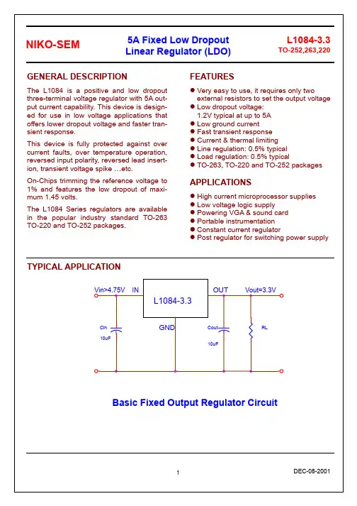
FeaturesAvailable in 1.5V, 1.8V, 2.5V, 3.3V version TO-252,TO-263 packageInternal short circuit current limiting Internal over temperature protectionOutput current 5AApplicationsPost regulation for switching DC/DC con-verterHigh efficiency linear regulator Battery powered instrumentationMotherboardGeneral DescriptionThe G1084-XX is a low dropout linear regulator with a dropout of 1.3V at 5A of load current. It is available in three fixed voltages: 1.5V, 1.8V, 2.5V and 3.3V. Refer to the G1084 for the adjustable version.The G1084-XX provides over temperature and over current protection circuits to prevent it from being damaged by abnormal operating conditions. The G1084-XX is available in TO-252 and TO-263 packages. A minimum of 220µF tantalum electro-lytic capacitor is required at the output to improve the transient response and stability.Ordering InformationPIN OPTIONORDER NUMBER ORDER NUMBER(Pb free)MARKINGTEMP. RANGEPACKAGE1 2 3G1084-15T43U G1084-15T43Uf G1084-15-40°C to +85°C TO-252 GND V OUT V IN G1084-18T43U G1084-18T43Uf G1084-18-40°C to +85°C TO-252 GND V OUT V IN G1084-25T43U G1084-25T43Uf G1084-25-40°C to +85°C TO-252 GND V OUT V IN G1084-33T43U G1084-33T43Uf G1084-33-40°C to +85°C TO-252 GND V OUT V IN G1084-15T53U G1084-15T53Uf G1084-15-40°C to +85°C TO-263 GND V OUT V IN G1084-18T53U G1084-18T53Uf G1084-18-40°C to +85°C TO-263 GND V OUT V IN G1084-25T53U G1084-25T53Uf G1084-25-40°C to +85°C TO-263 GND V OUT V ING1084-33T53U G1084-33T53Uf G1084-33-40°C to +85°CTO-263 GND V OUTV IN* For other package types and pin options, please contact us at sales @Order Number IdentificationTypePin Option Type Voltage Part NumberPACKAGE TYPEPIN OPTIONPACKINGT4: TO-252 12 3 U: Tape & Reel T5: TO-2633: GNDV OUTV INPackage Type Typical Application[Note 4]: Type of C OUT1V OUTµF23TO-252、TO-263Input Voltage . . . . . . . . . . . . . . . . . . . . . . . . . . . . . .8V Power Dissipation Internally Limited (Note 2) Maximum Junction Temperature . . . . . . . . . . . . . . .150°C Storage Temperature Range . . . . .-65°C ≤ T J≤+150°C Reflow Temperature (soldering, 10sec) . . . . . . 260°C Thermal Resistance Junction to AmbientTO-252(1) . . . . . . . . . . . . . . . . . . . . . . . . . . . . . 95°C/W TO-263(1) . . . . . . . . . . . . . . . . . . . . . . . . . . . . . 92°C/W Thermal Resistance Junction to CaseTO-252 . . . . . . . . . . . . . . . . . . . . . . . . . . . . . . . 8°C/W TO-263 . . . . . . . . . . . . . . . . . . . . . . . . . . . . . . ..6°C/W ESD Rating (Human Body Model) . . . . . . . . . . . . .2kV Note (1): See Recommended Minimum Footprint Input Voltage . . . . . . . . . . . . . . . . . . . . . . . . . .2.2V~7V Temperature Range . . . . . . . . . . . . . -40°C ≤ T A≤85°CElectrical CharacteristicsV IN = 5V, C IN = C OUT = 220µF, T A = T J = 25°C unless otherwise specified. (Note3)PARAMETER CONDITIONMINTYPMAX UNITOutput Voltage 10mA < I OUT < 5A -2% V O 2% VLine Regulation (V OUT + 0.7V) < V IN < 5.5V, I OUT = 10mA --- 0.1 --- %G1084-18 V IN = 3.8V, 10mA < I OUT < 5AG1084-25 V IN = 5V, 10mA < I OUT < 5ALoad RegulationG1084-33 V IN = 5V, 10mA < I OUT < 5A--- 1 --- %G1084-18 ΔV OUT = 2%, I OUT = 5A --- 1.6 ---G1084-25 ΔV OUT = 2%, I OUT = 5A --- 1.3 ---Dropout VoltageG1084-33 ΔV OUT = 2%, I OUT = 5A --- 1.1 ---VCurrent Limit (V IN - V OUT) = 2V --- 5.5 --- AShort Circuit Current --- 1 --- AG1084-18 V IN = 5V --- 1.7 ---G1084-25 V IN = 5V --- 2.1 ---Quiescent CurrentG1084-33 V IN = 5V --- 2.4 ---mARipple Rejection f = 120Hz, C OUT = 10µF Tantalum,(V IN - V OUT) = 3V, I OUT = 1A--- 50 --- dBThermal Shutdown Junction Temperature --- 150 --- °C Note 1: Absolute Maximum Ratings are limits beyond which damage to the device may occur. Operating Conditions are conditions under which the device functions but the specifications might not be guaranteed. For guaranteed specifications and test conditions see the Electrical Characteristics.Note 2: The maximum power dissipation is a function of the maximum junction temperature, T Jmax ; total thermal resistance, θJA, and ambient temperature T A. The maximum allowable power dissipation at any ambient temperature is T jmax-T A / θJA. If this dissipation is exceeded, the die temperature will rise above 150°C and IC will go into thermal shutdown.Note3: Low duty pulse techniques are used during test to maintain junction temperature as close to ambient as possible.Note4: The type of output capacitor should be tantalum or aluminum.DefinitionsDropout VoltageThe input/output Voltage differential at which the regulator output no longer maintains regulation against further reductions in input voltage. Measured when the output drops 2% below its nominal value. Dropout voltage is affected by junction temperature, load cur-rent and minimum input supply requirements.Line RegulationThe change in output voltage for a change in input voltage. The measurement is made under conditions of low dissipation or by using pulse techniques such that average chip temperature is not significantly af-fected. Load RegulationThe change in output voltage for a change in load current at constant chip temperature. The measure-ment is made under conditions of low dissipation or by using pulse techniques such that average chip tem-perature is not significantly affected.Maximum Power DissipationThe maximum total device dissipation for which the regulator will operate within specifications.Quiescent Bias CurrentCurrent which is used to operate the regulator chip and is not delivered to the load.VIN -VOUT= 3V, CIN = 220µF, C OUT = 220µF, T A =25°C, unless otherwise noted.Line Transient ResponseLoad Transient ResponseShort Circuit CurrentRipple RejectionG1084-33 Overcurrent Protection CharacteristicsG1084 Start-upG1084-18 Overcurrent Protection CharacteristicsG1084-18 Start-upG1084 Max. Power Dissipation vs. PCB Top Copper AreaG1084 Max. Power Dissipation vs. T A MBG1084-18 Quiescent Current vs. TemperatureG1084-18 Dropout Voltage vs. IG1084-18 Output Voltage vs. TemperatureG1084-33 Quiescent Current vs. Temperature G1084-33 Dropout Voltage vs. IG1084-33 Output Voltage vs. Temperature G1084-33 Output Voltage vs. ILRecommend Minimum FootprintTO-252TO-263TO-252 (T4) PackageMILLIMETER INCHSYMBOLMIN. MAX. MIN. MAX.A 2.19 2.38 0.086 0.094 A1 0.89 1.27 0.035 0.050 b 0.64 0.89 0.025 0.035 C 0.46 0.58 0.018 0.023 D 5.97 6.22 0.235 0.245 E 6.35 6.73 0.2500.265 E1 5.21 5.46 0.205 0.215e 2.26BSC 0.09BSC e1 3.96 5.18 0.156 0.204 F 0.46 0.58 0.018 0.023 L1 0.89 2.03 0.035 0.080 L2 0.64 1.02 0.025 0.040 L3 2.40 2.80 0.095 0.110 H 9.40 10.40 0.370 0.410 θ 0° 4° 0° 4°TO-263 (T5) PackageMILLIMETER INCH SYMBOLMIN MAX MIN MAXA 4.30 4.70 0.169 0.185 A1 1.22 1.32 0.048 0.055 A2 2.45 2.69 0.104 0.106 b 0.69 0.94 0.027 0.037 b1 1.22 1.40 0.048 0.055 C 0.36 0.56 0.014 0.022 D 8.64 9.652 0.340 0.380 E 9.7010.54 0.382 0.415 e 2.29 2.79 0.090 0.110 e1 4.83 5.33 0.190 0.210 H 14.60 15.78 0.575 0.625 L 4.70 5.84 0.185 0.230 L1 1.20 1.778 0.047 0.070 L2 2.24 2.84 0.088 0.111 L3 1.40MAX 0.055MAXTaping SpecificationPACKAGE Q’TY/REELTO-252 2,500 ea TO-263 800 eaGMT Inc. does not assume any responsibility for use of any circuitry described, no circuit patent licenses are implied and GMT Inc. reserves the right at any time without notice to change said circuitry and specifications.TO-252 Package OrientationTO-263 Package OrientationFeed DirectionFeed Direction。