
最新S3C2440处理器资料
- 格式:ppt
- 大小:1.56 MB
- 文档页数:41

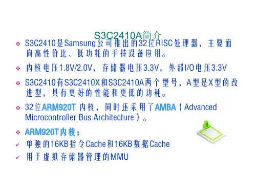


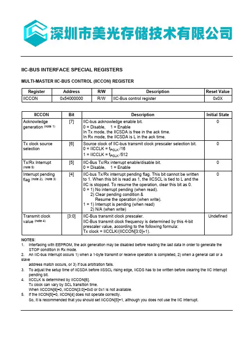
IIC-BUS INTERFACE SPECIAL REGISTERSMULTI-MASTER IIC-BUS CONTROL (IICCON) REGISTERRegister Address R/W DescriptionReset ValueIICCON0x54000000R/WIIC-Bus control register0x0XIICCON Bit DescriptionInitial StateAcknowledge generation (note 1)[7]IIC-bus acknowledge enable bit.0 = Disable, 1 = EnableIn Tx mode, the IICSDA is free in the ack time.In Rx mode, the IICSDA is L in the ack time.Tx clock source selection [6]Source clock of IIC-bus transmit clock prescaler selection bit.0 = IICCLK = f PCLK /161 = IICCLK = f PCLK /512Tx/Rx Interrupt(note 5)[5]IIC-Bus Tx/Rx interrupt enable/disable bit.0 = Disable, 1 = Enable0Interrupt pending flag (note 2), (note 3)[4]IIC-bus Tx/Rx interrupt pending flag. This bit cannot be written to 1. When this bit is read as 1, the IICSCL is tied to L and the IIC is stopped. To resume the operation, clear this bit as 0.0 = 1) No interrupt pending (when read).2)Clear pending condition &Resume the operation (when write).1 = 1) Interrupt is pending (when read)2)N/A (when write)0Transmit clock value (note 4)[3:0]IIC-Bus transmit clock prescaler.IIC-Bus transmit clock frequency is determined by this 4-bit prescaler value, according to the following formula:Tx clock = IICCLK/(IICCON[3:0]+1).UndefinedNOTES:1.Interfacing with EEPROM, the ack generation may be disabled before reading the last data in order to generate theSTOP condition in Rx mode.2.An IIC-bus interrupt occurs 1) when a 1-byte transmit or receive operation is completed, 2) when a general call or a slaveaddress match occurs, or 3) if bus arbitration fails.3.To adjust the setup time of IICSDA before IISSCL rising edge, IICDS has to be written before clearing the IIC interruptpending bit.4.IICCLK is determined by IICCON[6].Tx clock can vary by SCL transition time.When IICCON[6]=0, IICCON[3:0]=0x0 or 0x1 is not available.5.If the IICON[5]=0, IICON[4] does not operate correctly.So, It is recommended that you should set IICCON[5]=1, although you does not use the IIC interrupt.IIC-BUS INTERFACES3C2410XMULTI-MASTER IIC-BUS CONTROL/STATUS (IICSTAT) REGISTERRegister Address R/W DescriptionReset ValueIICSTAT0x54000004R/WIIC-Bus control/status register0x0IICSTAT Bit DescriptionInitial StateMode selection[7:6]IIC-bus master/slave Tx/Rx mode select bits.00: Slave receive mode 01: Slave transmit mode 10: Master receive mode 11: Master transmit mode00Busy signal status /START STOP condition[5]IIC-Bus busy signal status bit.0 = read) Not busy (when read) write) STOP signal generation 1 = read) Busy (when read)write) START signal generation.The data in IICDS will be transferred automatically just after the start signal.0Serial output [4]IIC-bus data output enable/disable bit.0 = Disable Rx/Tx, 1 = Enable Rx/Tx 0Arbitration status flag[3]IIC-bus arbitration procedure status flag bit.0 = Bus arbitration successful1 = Bus arbitration failed during serial I/O 0Address-as-slave status flag[2]IIC-bus address-as-slave status flag bit.0 = Cleared when START/STOP condition was detected1 = Received slave address matches the address value in the IICADDAddress zero status flag[1]IIC-bus address zero status flag bit.0 = Cleared when START/STOP condition was detected.1 = Received slave address is 00000000b.0Last-received bit status flag[0]IIC-bus last-received bit status flag bit.0 = Last-received bit is 0 (ACK was received).1 = Last-received bit is 1 (ACK was not received).S3C2410X IIC-BUS INTERFACEIIC-BUS INTERFACE S3C2410XS3C2410X SPI INTERFACESPI SPECIAL REGISTERSSPI CONTROL REGISTERRegister Address R/W Description Reset Value SPCON00x59000000R/W SPI channel 0 control register0x00 SPCON10x59000020R/W SPI channel 1 control register0x00SPCONn Bit Description Initial StateSPI Mode Select (SMOD)[6:5]Determine how and by what SPTDAT is read/written.00 = polling mode, 01 = interrupt mode10 = DMA mode, 11 = reserved00SCK Enable (ENSCK)[4]Determine whether you want SCK enable or not (for onlymaster).0 = disable, 1 = enableMaster/Slave Select (MSTR)[3]Determine the desired mode (master or slave).0 = slave, 1 = masterNOTE: In slave mode, there should be set up time formaster to initiate Tx/Rx.Clock Polarity Select (CPOL)[2]Determine an active high or active low clock.0 = active high, 1 = active lowClock Phase Select (CPHA)[1]Select one of two fundamentally different transfer formats.0 = format A, 1 = format BTx Auto Garbage Data mode enable (TAGD)[0]Decide whether the receiving data only needs or not.0 = normal mode, 1 = Tx auto garbage data modeNOTE: In normal mode, if you only want to receive data,you should transmit dummy 0xFF data.。