光电子学 chapter 3精品PPT课件
- 格式:pptx
- 大小:1.51 MB
- 文档页数:49

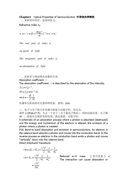
Chapter1 Optical Properties of Semiconductors 半导体光学特性 一.复折射率的实,虚部的意义: Refractive index n r21/2'''0/()r r r c n c v i n in σμεω==+=+ '''r r The real part of index n speed of lightThe imaginary part of index n attenuation of light↔↔二.折射率与增益吸收系数的关系: Absorption coefficient αThe absorption coefficient αis described by the absorption of the intensity.00(),(),1z z I z I e dI I e dz dI I dzαααα--==-⇒=-传播单位距离相对光强的吸收量。
量纲:/cm.三.电子与光子相互作用遵守能量与动量守恒:表达式: 课件1-1P16,17图:失去一个光子(光子被电子吸收),得到动量改变,光子数减一,能量从光场转变到电场,满足能量,动量守恒。
A schematic of an absorption process where a photon is absorbed (destroyed) and the energy and momentum of the electron is altered; the emission of a photon where a photon is created.P18, Band to band absorption and emission in semiconductors. An electron in the valence band absorbs a photon and moves into the conduction band; In the reverse process an electron in the conduction band emits a photon and moves "vertically" down into the valence band. Direct Interband TransitionsReduced e —h mass ( 折合质量 ) The interaction can cause absorption or 222222*11()()211()22C V e hg e h rk E E m m k E m m k m ωω****=-++-=+= *r memission of photons.The absorption process is proportional to the photon density ph n比较本征吸收与非本征吸收的条件,类型:Conditions: 本征吸收:光子能量大于材料带隙;非本征吸收:光子能量小于材料带隙。