LM3S6432-IBZ50-A2T系列 规格书,Datasheet 资料
- 格式:pdf
- 大小:349.22 KB
- 文档页数:16
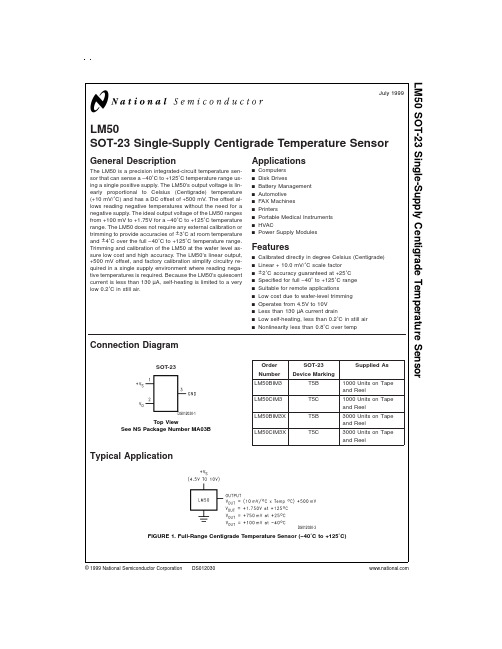
LM50SOT-23Single-Supply Centigrade Temperature SensorGeneral DescriptionThe LM50is a precision integrated-circuit temperature sen-sor that can sense a −40˚C to +125˚C temperature range us-ing a single positive supply.The LM50’s output voltage is lin-early proportional to Celsius (Centigrade)temperature (+10mV/˚C)and has a DC offset of +500mV.The offset al-lows reading negative temperatures without the need for a negative supply.The ideal output voltage of the LM50ranges from +100mV to +1.75V for a −40˚C to +125˚C temperature range.The LM50does not require any external calibration or trimming to provide accuracies of ±3˚C at room temperature and ±4˚C over the full −40˚C to +125˚C temperature range.Trimming and calibration of the LM50at the wafer level as-sure low cost and high accuracy.The LM50’s linear output,+500mV offset,and factory calibration simplify circuitry re-quired in a single supply environment where reading nega-tive temperatures is required.Because the LM50’s quiescent current is less than 130µA,self-heating is limited to a very low 0.2˚C in still air.Applicationsn Computers n Disk Drivesn Battery Management n Automotive n FAX Machines n Printersn Portable Medical Instruments n HVACnPower Supply ModulesFeaturesn Calibrated directly in degree Celsius (Centigrade)n Linear +10.0mV/˚C scale factor n ±2˚C accuracy guaranteed at +25˚C n Specified for full −40˚to +125˚C range n Suitable for remote applicationsn Low cost due to wafer-level trimming n Operates from 4.5V to 10V n Less than 130µA current drainn Low self-heating,less than 0.2˚C in still air nNonlinearity less than 0.8˚C over tempConnection DiagramOrder SOT-23Supplied As Number Device MarkingLM50BIM3T5B 1000Units on Tape and ReelLM50CIM3T5C 1000Units on Tape and ReelLM50BIM3X T5B 3000Units on Tape and ReelLM50CIM3XT5C3000Units on Tape and ReelTypical ApplicationSOT-23DS012030-1Top ViewSee NS Package Number MA03BDS012030-3FIGURE 1.Full-Range Centigrade Temperature Sensor (−40˚C to +125˚C)July 1999LM50SOT-23Single-Supply Centigrade Temperature Sensor©1999National Semiconductor Corporation Absolute Maximum Ratings(Note1)Supply Voltage+12V to−0.2V Output Voltage(+V S+0.6V)to−1.0V Output Current10mA Storage Temperature−65˚C to+150˚C Lead Temperature:SOT Package(Note2):Vapor Phase(60seconds)215˚C Infrared(15seconds)220˚C T JMAX,MaximumJunction Temperature150˚C ESD Susceptibility(Note3):Human Body ModelMachine Model2000V250V Operating Ratings(Note1)Specified Temperature Range:T MIN to T MAX LM50C−40˚C to+125˚C LM50B−25˚C to+100˚C Operating Temperature Range−40˚C to+150˚C θJA(Note4)450˚C/W Supply Voltage Range(+V S)+4.5V to+10VElectrical CharacteristicsUnless otherwise noted,these specifications apply for V S=+5V DC and I LOAD=+0.5µA,in the circuit of Figure1.Boldface limits apply for the specified T A=T J=T MIN to T MAX;all other limits T A=T J=+25˚C,unless otherwise noted.Parameter Conditions LM50B LM50C Units(Limit)Typical Limit Typical Limit(Note5)(Note5)Accuracy T A=+25˚C±2.0±3.0˚C(max) (Note6)T A=T MAX±3.0±4.0˚C(max)T A=T MIN+3.0,−3.5±4.0˚C(max) Nonlinearity(Note7)±0.8±0.8˚C(max) Sensor Gain+9.7+9.7mV/˚C(min) (Average Slope)+10.3+10.3mV/˚C(max) Output Resistance2000400020004000Ω(max) Line Regulation+4.5V≤V S≤+10V±0.8±0.8mV/V(max) (Note8)±1.2±1.2mV/V(max) Quiescent Current+4.5V≤V S≤+10V130130µA(max) (Note9)180180µA(max) Change of Quiescent+4.5V≤V S≤+10V 2.0 2.0µA(max) Current(Note9)Temperature Coefficient of+1.0+2.0µA/˚C Quiescent CurrentLong Term Stability(Note10)T J=125˚C,for±0.08±0.08˚C1000hoursNote1:Absolute Maximum Ratings indicate limits beyond which damage to the device may occur.DC and AC electrical specifications do not apply when operating the device beyond its rated operating conditions.Note2:See AN-450“Surface Mounting Methods and Their Effect on Product Reliability”or the section titled“Surface Mount”found in a current National Semicon-ductor Linear Data Book for other methods of soldering surface mount devices.Note3:Human body model,100pF discharged through a1.5kΩresistor.Machine model,200pF discharged directly into each pin.Note4:Thermal resistance of the SOT-23package is specified without a heat sink,junction to ambient.Note5:Limits are guaranteed to National’s AOQL(Average Outgoing Quality Level).Note6:Accuracy is defined as the error between the output voltage and10mv/˚C times the device’s case temperature plus500mV,at specified conditions of volt-age,current,and temperature(expressed in˚C).Note7:Nonlinearity is defined as the deviation of the output-voltage-versus-temperature curve from the best-fit straight line,over the device’s rated temperature range.Note8:Regulation is measured at constant junction temperature,using pulse testing with a low duty cycle.Changes in output due to heating effects can be com-puted by multiplying the internal dissipation by the thermal resistance.Note9:Quiescent current is defined in the circuit of Figure1.Note10:For best long-term stability,any precision circuit will give best results if the unit is aged at a warm temperature,and/or temperature cycled for at least46 hours before long-term life test begins.This is especially true when a small(Surface-Mount)part is wave-soldered;allow time for stress relaxation to occur.The ma-jority of the drift will occur in the first1000hours at elevated temperatures.The drift after1000hours will not continue at the first1000hour rate.2Typical Performance Characteristics To generate these curves the LM50was mounted to a printed circuit board as shown in Figure2.Thermal ResistanceJunction to AirDS012030-21Thermal Time ConstantDS012030-22Thermal Response in Still Airwith Heat Sink(Figure2)DS012030-23Thermal Responsein Stirred Oil Bathwith Heat SinkDS012030-24Start-Up Voltagevs TemperatureDS012030-25Thermal Response in StillAir without a Heat SinkDS012030-26Quiescent Current vs Temperature(Figure1)DS012030-27Accuracy vs TemperatureDS012030-28Noise VoltageDS012030-29 3Typical Performance CharacteristicsTo generate these curves the LM50was mounted to a printedcircuit board as shown in Figure 2.(Continued)1.0MountingThe LM50can be applied easily in the same way as other integrated-circuit temperature sensors.It can be glued or ce-mented to a surface and its temperature will be within about 0.2˚C of the surface temperature.This presumes that the ambient air temperature is almost the same as the surface temperature;if the air temperature were much higher or lower than the surface temperature,the ac-tual temperature of the LM50die would be at an intermediate temperature between the surface temperature and the air temperature.To ensure good thermal conductivity the backside of the LM50die is directly attached to the GND pin.The lands and traces to the LM50will,of course,be part of the printed cir-cuit board,which is the object whose temperature is being measured.These printed circuit board lands and traces will not cause the LM50s temperature to deviate from the de-sired temperature.Alternatively,the LM50can be mounted inside a sealed-end metal tube,and can then be dipped into a bath or screwed into a threaded hole in a tank.As with any IC,the LM50and accompanying wiring and circuits must be kept insulated and dry,to avoid leakage and corrosion.This is especially true if the circuit may operate at cold temperatures where conden-sation can occur.Printed-circuit coatings and varnishes suchas Humiseal and epoxy paints or dips are often used to en-sure that moisture cannot corrode the LM50or its connec-tions.Temperature Rise of LM50Due to Self-Heating (Thermal Resistance,θJA )SOT-23SOT-23no heat sink *small heat fin **Still air 450˚C/W260˚C/W Moving air180˚C/W*Part soldered to 30gauge wire.**Heat sink used is 1⁄2"square printed circuit board with 2oz.foil with part at-tached as shown in Figure 2.2.0Capacitive LoadsThe LM50handles capacitive loading very well.Without any special precautions,the LM50can drive any capacitive load.The LM50has a nominal 2k Ωoutput impedance (as can be seen in the block diagram).The temperature coefficient of the output resistors is around 1300ppm/˚C.Taking into ac-count this temperature coefficient and the initial tolerance of the resistors the output impedance of the LM50will not ex-ceed 4k Ω.In an extremely noisy environment it may be nec-essary to add some filtering to minimize noise pickup.It is recommended that 0.1µF be added from V IN to GND to by-Supply Voltage vs Supply CurrentDS012030-30Start-Up ResponseDS012030-31DS012030-19FIGURE 2.Printed Circuit Board Used for Heat Sink to Generate All Curves.1⁄2"Square Printed Circuit Boardwith 2oz.Foil or SimilarDS012030-7FIGURE 3.LM50No Decoupling Requiredfor Capacitive LoadDS012030-8FIGURE 4.LM50C with Filter for Noisy Environment 42.0Capacitive Loads(Continued)pass the power supply voltage,as shown in Figure 4.In a noisy environment it may be necessary to add a capacitor from the output to ground.A 1µF output capacitor with the 4k Ωoutput impedance will form a 40Hz lowpass filter.Sincethe thermal time constant of the LM50is much slower than the 25ms time constant formed by the RC,the overall re-sponse time of the LM50will not be significantly affected.For much larger capacitors this additional time lag will increase the overall response time of the LM50.3.0Typical ApplicationsDS012030-17*R2≈2k with a typical 1300ppm/˚C drift.FIGURE 5.Block DiagramDS012030-11FIGURE 6.Centigrade Thermostat/Fan ControllerDS012030-13FIGURE 7.Temperature To Digital Converter (Serial Output)(+125˚C Full Scale)53.0Typical Applications(Continued)DS012030-14FIGURE8.Temperature To Digital Converter(Parallel TRI-STATE®Outputs forStandard Data Bus toµP Interface)(125˚C Full Scale)DS012030-16FIGURE9.LM50With Voltage-To-Frequency Converter And Isolated Output(−40˚C to+125˚C;100Hz to1750Hz)6Physical Dimensions inches(millimeters)unless otherwise notedLIFE SUPPORT POLICYNATIONAL’S PRODUCTS ARE NOT AUTHORIZED FOR USE AS CRITICAL COMPONENTS IN LIFE SUPPORT DEVICES OR SYSTEMS WITHOUT THE EXPRESS WRITTEN APPROVAL OF THE PRESIDENT AND GENERAL COUNSEL OF NATIONAL SEMICONDUCTOR CORPORATION.As used herein:1.Life support devices or systems are devices orsystems which,(a)are intended for surgical implantinto the body,or(b)support or sustain life,andwhose failure to perform when properly used inaccordance with instructions for use provided in thelabeling,can be reasonably expected to result in asignificant injury to the user.2.A critical component is any component of a lifesupport device or system whose failure to performcan be reasonably expected to cause the failure ofthe life support device or system,or to affect itssafety or effectiveness.National SemiconductorCorporationAmericasTel:1-800-272-9959Fax:1-800-737-7018Email:support@National SemiconductorEuropeFax:+49(0)180-5308586Email:europe.support@Deutsch Tel:+49(0)180-5308585English Tel:+49(0)180-5327832Français Tel:+49(0)180-5329358Italiano Tel:+49(0)180-5341680National SemiconductorAsia Pacific CustomerResponse GroupTel:65-2544466Fax:65-2504466Email:sea.support@National SemiconductorJapan Ltd.Tel:81-3-5639-7560Fax:81-3-5639-7507 SOT-23Molded Small Outline Transistor Package(M3)Order Number LM50BIM3,or LM50CIM3NS Package Number MA03BLM50SOT-23Single-SupplyCentigradeTemperatureSensor National does not assume any responsibility for use of any circuitry described,no circuit patent licenses are implied and National reserves the right at any time without notice to change said circuitry and specifications.。

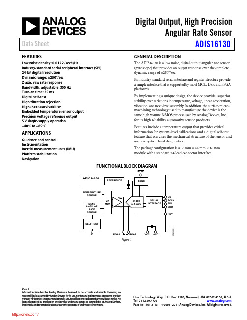
Digital Output, High PrecisionAngular Rate Sensor Data Sheet ADIS16130Rev. CInformation furnished by Analog Devices is believed to be accurate and reliable. However, noresponsibility is assumed by Analog Devices for its use, nor for any infringements of patents or other rights of third parties that may result from its use. Specifications subject to change without notice. No license is granted by implication or otherwise under any patent or patent rights of Analog Devices. T rademarks and registered trademarks are the property of their respective owners. One Technology Way, P.O. Box 9106, Norwood, M A 02062-9106, U.S.A. Tel: 781.329.4700 Fax: 781.461.3113 ©2008–2011 Analog Devices, Inc. All rights reserved.FEATURESLow noise density: 0.0125o/sec/√HzIndustry-standard serial peripheral interface (SPI) 24-bit digital resolutionDynamic range: ±250o/secZ-axis, yaw rate responseBandwidth, adjustable: 300 HzTurn-on time: 35 msDigital self-testHigh vibration rejectionHigh shock survivabilityEmbedded temperature sensor output Precision voltage reference output5 V single-supply operation−40°C to +85°CAPPLICATIONSGuidance and controlInstrumentationInertial measurement units (IMU)Platform stabilizationNavigation GENERAL DESCRIPTIONThe ADIS16130 is a low noise, digital output angular rate sensor (gyroscope) that provides an output response over the complete dynamic range of ±250o/sec.Its industry-standard serial interface and register structure provide a simple interface that is supported by most MCU, DSP, and FPGA platforms.By implementing a unique design, the device provides superior stability over variations in temperature, voltage, linear acceleration, vibration, and next-level assembly. In addition, the surface-micro-machining technology used to manufacture the device is the same high volume BiMOS process used by Analog Devices, Inc., for its high reliability automotive sensor products.Features include a temperature output that provides critical information for system-level calibrations and a digital self-test feature that exercises the mechanical structure of the sensor and enables system-level diagnostics.The package configuration is a 36 mm × 44 mm × 16 mm module with a standard 24-lead connector interface.FUNCTIONAL BLOCK DIAGRAMSYNCFigure 1.ADIS16130Data SheetRev. C | Page 2 of 16TABLE OF CONTENTSFeatures..............................................................................................1 Applications.......................................................................................1 General Description.........................................................................1 Functional Block Diagram..............................................................1 Revision History...............................................................................2 Specifications.....................................................................................3 Timing Specifications..................................................................4 Absolute Maximum Ratings............................................................6 Thermal Resistance......................................................................6 ESD Caution..................................................................................6 Pin Configuration and Function Descriptions.............................7 Typical Performance Characteristics.............................................8 Basic Operation.................................................................................9 Quick Start.....................................................................................9 Data Format................................................................................10 Configuration Options..............................................................10 Control Registers............................................................................11 Control Register Details............................................................11 Applications Information..............................................................12 Achieving Optimal Noise Performance..................................12 Second-Level Assembly.............................................................12 Outline Dimensions.......................................................................13 Ordering Guide.. (13)REVISION HISTORY9/11—Rev. B to Rev. CChanges to Ordering Guide (13)8/10—Rev. A to Rev. BChanges to Table 1............................................................................3 Changes to Configuration Sequence Section................................9 Added Data Format Section, Table 7, and Table 8 (10)3/08—Rev. 0 to Rev. AChanges to Figure 15......................................................................10 Changes to Ordering Guide. (13)1/08—Revision 0: Initial VersionData Sheet ADIS16130SPECIFICATIONST A = 25°C, VCC = 5 V, angular rate = 0°/sec, C OUT = 0 μF, ±1 g, unless otherwise noted.1 All minimum and maximum specifications are guaranteed. Typical specifications are not tested or guaranteed.2 Dynamic range is the maximum full-scale measurement range possible, including output swing range, initial offset, sensitivity, offset drift, and sensitivity drift at 4.75 V to 5.25 V supplies.3 Resulting bias stability is <0.01°/sec.4 Self-test response varies with temperature; see Figure 12.Rev. C | Page 3 of 16ADIS16130 Data SheetTIMING SPECIFICATIONSAll input signals are specified with 10% to 90% rise and fall times of less than 5 ns.1 These numbers are measured with the load circuit shown in Figure 4 and defined as the time required for the output to cross the V OL or V OH limits.2 This specification is relevant only if CS goes low while SCLK is low.3 These numbers are derived from the measured time taken by the data output to change 0.5 V when loaded with the circuit shown in Figure 4. The measured number is then extrapolated back to remove effects of charging or discharging the 50 pF capacitor. Therefore, the times quoted are the true bus relinquish times of the part and as such are independent of external bus loading capacitances.Rev. C | Page 4 of 16Data SheetADIS16130Rev. C | Page 5 of 16SDISCLKCS07238-002Figure 2. Input Timing for Write Operation07238-003Figure 3. Output Timing for Read OperationDD = 5VDD = 3V)DD = 5VDD = 3V)1.6V07328-024Figure 4. Load Circuit for Access Time and Bus Relinquish TimeADIS16130Data SheetRev. C | Page 6 of 16ABSOLUTE MAXIMUM RATINGSTHERMAL RESISTANCETable 3.ParameterRating Acceleration (Any Axis, Unpowered, 0.5 ms) 2000 g Acceleration (Any Axis, Powered, 0.5 ms) 2000 g+V S−0.3 V to +6.0 V Output Short-Circuit Duration (Any Pin to Common)Indefinite Operating Temperature Range −40°C to +85°C Storage Temperature Range −65°C to +150°CThe ADIS16130 provides a temperature output that isrepresentative of the junction temperature. This can be used for system-level monitoring and power management/thermal characterization.Table 4. Thermal CharacteristicsPackage Type 1 θJA θJC Unit 24-Lead Module15.7 1.48 °C/W1Weight = 28.5 g typical.Stresses above those listed under Absolute Maximum Ratings may cause permanent damage to the device. This is a stress rating only; functional operation of the device at these or any other conditions above those indicated in the operationalsection of this specification is not implied. Exposure to absolute maximum rating conditions for extended periods may affect device reliability.RATE+07238-026Dropping the device onto a hard surface may cause a shock of greater than 2000 g and exceed the absolute maximum rating of the device. Care should be exercised when handling the device to avoid damage.Figure 5. Rotational Measurement OrientationESD CAUTIONData SheetADIS16130Rev. C | Page 7 of 16PIN CONFIGURATION AND FUNCTION DESCRIPTIONSS TS TS TS TS TV C CV C CV C CG N DG N DG N DR O A 107328-004Figure 6. Pin ConfigurationADIS16130Data SheetRev. C | Page 8 of 16TYPICAL PERFORMANCE CHARACTERISTICS2.52.01.51.00.50–0.5–1.0–1.5–2.0–2.5–60–40–202040608010012007328-018B I A S S H I F T (°/s e c )TEMPERATURE (°C)σσµFigure 7. Bias Shift vs. Temperature, VCC = 5 V1.000.750.500.250–0.25–0.50–0.75–1.00–60–40–2002040608010012007328-019S E N S I T I V I T Y E R R O R (%)TEMPERATURE (°C)Figure 8. Sensitivity Error vs. Temperature, VCC = 5 V 0.050–0.05–0.10–0.154.755.05.2507328-020S E N S I T I V I T Y E R R O R (%)POWER SUPPLY (V)Figure 9. Sensitivity Error vs. Power Supply, 25°C 0.010.00107328-021R O O T A L L E N V A R I A N C E (°/s e c )INTEGRATION TIME, (sec)Figure 10. Root Allen Variance, VCC = 5 V, 25°C21–1–205010015020025030035040007328-022S E N S I T I V I T Y E R R O R (%)ANGULAR RATE (°/sec)Figure 11. Sensitivity Error vs. Angular Rate, VCC = 5 V, 25°C90858075706560–60–40–2002040806010012007328-023S E L F -T E S T R E S P O N S E (°/s e c )TEMPERATURE (°C)Figure 12. Self-Test Response vs. Temperature, VCC = 5 VData SheetADIS16130Rev. C | Page 9 of 16BASIC OPERATIONThe ADIS16130 produces digital angular rate (RATE) andtemperature (TEMP) data. The digital communication employs a simple 4-wire SPI that provides access to output data and several configuration features. A set of communication and configuration registers govern the operation in the ADIS16130. See Table 10 for a summary of these registers.QUICK STARTThe ADIS16130 SPI operates in 8-bit segments. The first byte of a SPI sequence goes into the COM register, which contains the read/write control bit and the address of the target register. When writing information into control registers, the next byte contains the configuration information. When reading output data, the next one to three bytes contain the contents of the register selected.Configuration SequenceThe sequence in Table 6 provides the recommended configuration sequence. Table 2 and Figure 2 provide the timing information for each segment of this configuration sequence.For additional information on design and optimization with the ADIS16130, see the AN-1042 Application Note. Table 6. Configuration SequenceStep SDI 1 Register Purpose 1 0x01 COM Start a write sequence for IOP.2 0x38 I OP Configure the data-ready signal topulse low when the RATEDATA and TEMPDATA output registerscontain new data. The data-ready signal goes high after reading either of these registers.3 0x28 COM Start a write sequence for theRATECS register.4 0x0A RATECS Enable and configure thegyroscope data channel.5 0x30 COM Start a write sequence forRATECONV register.6 0x05 RATECONV Initialize the RATE conversion.7 0x2A COM Start a write sequence for theTEMPCS register.8 0x0A TEMPCS Enable and configure thetemperature data channel.9 0x32 COM Start a write sequence forTEMPCONV.10 0x05 TEMPCONV Initialize the TEMP conversion. 11 0x38 COM Start a write sequence for theMODE register.12 0x22 MODE Establish the data outputresolution to 24 bits and start the conversion process with the RATEDATA channel.1The SDI column lists the hexadecimal code representation of the SDI bit input sequence.Reading RATE Output DataAfter the configuration sequence in Table 6 is complete, reading the output data is very simple. The ADIS16130 converts the RATE and TEMP data continuously. To better understand this process, Figure 13 provides an example read sequence, and Table 2 and Figure 3 provide critical timing details for the output signal. The first byte of the sequence uses SDI to establish a read of the RATE output register. This is accomplished by writing 0x48 to the COM register. The most significant byte is first in the SDO sequence, followed by the next significant, and then the least significant. When 16-bit resolution is in use, only two bytes are output from the SDO during the read sequence.0x48DATA SCLK SDO SDI RDYDATA DATA07328-005Figure 13. Read Sequence ExampleThe data-ready signal, RDY , indicates that unread data is available on both RATE and TEMP output registers. After the RATE or TEMP channel is read, the signal returns high, as shown in . The RATE and TEMP channels update sequentially, and each has a sample rate of 5.7 kSPS. Theinternal sample rate is not dependent on the SPI signals or read rates. Using the data-ready signal to drive data collection helps avoid losing data due to data collision, which is when a user-driven read cycle coincides with the internal update time. In this case, the old data remains and the new data is lost. Figure 13If a lower sample rate meets system-level requirements, the data-ready signal can still be useful in facilitating SPI read sequences. In this case, the data-ready signal pulses high for approximately 26 μs before returning low and then repeats this pattern at two times the internal sample rate. This signal can feed a counter circuit (or firmware), which drives a processor interrupt routine at a reduced sample rate.Reading TEMP Output DataReading TEMP data requires a sequence that is very similar to that of Figure 13, except that the initial SDI sequence must be changed from 0x48 to 0x4A. If the TEMP data is not used, Step 7 to Step 10 of the configuration sequence are not required.ADIS16130Data SheetRev. C | Page 10 of 16DATA FORMATThe ADIS16130 uses the offset binary data format.⎥⎦⎤⎢⎣⎡°+−=⎥⎦⎤⎢⎣⎡−=C 25093,142488,2322323Codes TEMP Codes RATE Table 7. Gyroscope Rate Output Data Format24-Bit (Codes) 16-Bit (Codes)Rate Output 14,260,608 55,706 +250°/sec 8,623,488 33,686 +10°/sec8.388,612 32,769 +0.00017030°/sec 8,388,609+0.000042575°/sec 8,388,608 32,768 08,388,607−0.000042575°/sec 8,388,604 32,767 −0.00017030°/sec 8,153,728 31,850 −10°/sec 2,516,608 9,830−250°/secTable 8. Gyroscope Temperature Output Data Format24-Bit (Codes) 16-Bit (Codes) Rate Output 9,516,048 37,172 +105°C 9,234,188 36,071 +85°C 8,402,701 32,823 +26°C 8,388,608 32,768 +25°C 8,036,283 31,392 +0°C 7,472,563 29,189−40°CCONFIGURATION OPTIONSSynchronization InputThe SYNC pin can be used to synchronize the ADIS16130 with other devices in the system. When the SYNC bit in the I/O port register (IOP) is set and the SYNC pin is low, the ADIS16130 does not process any conversions. Instead, it waits until the SYNC pin goes high, and then starts the operation. This allows the conversion to start from a known point in time (for example, the rising edge of the SYNC pin).Self-Test FunctionThe self-test function enables system-level diagnostic checks for theentire ADIS16130 sensor/signal conditioning circuit. To activate the self-test function, there must be a logic high signal on all ST pins (see Table 5). When activated, the self-test function results in a rate measurement shift. By comparing the observed shift with the limits specified in this data sheet, users can determine the pass/fail criteria for system-level diagnostic routines. For normal gyroscope operation, place a logic low input onall ST pins. For systems that do not require this feature, tie all ST pins to GND.Analog BandwidthThe typical −3 dB cutoff frequency for the ADIS16130 is 300 Hz, which is the combined response of two single-polefilters, as shown in Figure 14. Pin ROA1 and Pin ROA2 providethe opportunity for further bandwidth reduction in the first filter stage, as shown in the following relationship:()ext dB C C R f +××π×=−213where: R = 25 kΩ. C = 6800 pF.C ext is as defined in Figure 15 and Table 9.The relationship between the −3 dB cutoff frequency and the external capacitance of the ADIS16130 is shown in Figure 15 and Table 9.07328-006Figure 14. Frequency Response Block DiagramFREQUENCY (Hz)0–1–2–3–4–5–6–7–8–9–10A M P L I T U D E (dB )07328-007Figure 15. Frequency Response: C ext = 0 μF vs. C ext = 0.15 μFTable 9. Nominal Bandwidth for Standard Capacitor ValuesC ext (pF) BW (Hz) C ext (pF) BW (Hz) C ext (pF) BW (Hz) 1000 276.8 10,000 198.9 100,000 52.2 1200 274.4 12,000 187.2 120,000 44.8 1500 270.9 15,000 172.1 150,000 37.0 1800 267.5 18,000 159.2 180,000 31.5 2200 263.1 22,000 144.7 220,000 26.3 2700 257.7 27,000 129.9 270,000 21.8 3300 251.6 33,000 115.7 330,000 18.1 3900 245.8 39,000 104.4 390,000 15.5 4300 242.1 43,000 97.9 430,000 14.1 4700 238.4 47,000 92.3 470,000 12.9 5100 234.9 51,000 87.2 510,000 12.0 5600 230.7 56,000 81.6 560,000 10.9 6200 225.8 62,000 75.8 620,000 9.9 7500 215.8 75,000 65.6 750,000 8.2 8200 210.8 82,000 61.2 820,000 7.6 9100 204.7 91,000 56.3 910,000 6.8分销商库存信息: ANALOG-DEVICES ADIS16130AMLZ。

17A 、55V N 沟道增强型场效应管描述SVDZ24NT N 沟道增强型功率MOS 场效应晶体管,采用士兰微电子新的平面VDMOS 工艺技术制造。
先进的工艺及条状的原胞设计结构使得该产品具有较低的导通电阻、优越的开关性能及很高的雪崩击穿耐量。
该产品可广泛应用于电子镇流器,低功率开关电源。
特点♦ 17A ,55V ,R DS(on)(典型值)=45m Ω@V GS =10V ♦ 低栅极电荷量 ♦ 低反向传输电容 ♦ 开关速度快 ♦提升了dv/dt 能力产品规格分类产 品 名 称 封装形式 打印名称 材料 包装 SVDZ24NTTO-220-3LSVDZ24NT无铅料管极限参数(除非特殊说明,T C =25°C)参 数符 号 参数范围 单位 漏源电压 V DS 55 V 栅源电压 V GS ±20 V 漏极电流 T C =25°C I D 17 A T C =100°C12 漏极脉冲电流 I DM 68 A 耗散功率(T C =25°C ) - 大于25°C 每摄氏度减少 P D 45 W 0.36 W/°C 单脉冲雪崩能量(注1) E AS 122 mJ 工作结温范围 T J -55~+175 °C 贮存温度范围T stg-55~+175°C热阻特性参 数符 号 参数范围 单位 芯片对管壳热阻 R θJC 2.78 °C/W 芯片对环境的热阻R θJA62.5°C/W电性参数(除非特殊说明,TC=25°C)参数符号测试条件最小值典型值最大值单位漏源击穿电压B VDSS V GS=0V,I D=250µA 55 -- -- V 漏源漏电流I DSS V DS=55V,V GS=0V -- -- 20 µA 栅源漏电流I GSS V GS=±20V,V DS=0V -- -- ±100 nA 栅极开启电压V GS(th)V GS= V DS,I D=250µA 2.0 -- 4.0 V 导通电阻R DS(on)V GS=10V,I D=10A -- 45 70 mΩ输入电容C issV DS=25V,V GS=0V,f=1.0MHz -- 400 --pF输出电容C oss-- 130 -- 反向传输电容C rss-- 12.5 --开启延迟时间t d(on)V DD=28V,V GS=10V,R G=25Ω,I D=10A(注2,3) -- 5.4 --ns开启上升时间t r-- 32.5 -- 关断延迟时间t d(off)-- 22.1 -- 关断下降时间t f-- 12.4 --栅极电荷量Q g V DD=44V,V GS=10V,I D=10A(注2,3) -- 10.5 --nC栅极-源极电荷量Q gs-- 2.5 --栅极-漏极电荷量Q gd-- 4.0 --源-漏二极管特性参数参数符号测试条件最小值典型值最大值单位源极电流I S MOS管中源极、漏极构成的反偏P-N结-- -- 17A源极脉冲电流I SM-- -- 68源-漏二极管压降V SD I S=10A,V GS=0V -- -- 1.3 V反向恢复时间T rr I S=10A,V GS=0V,dI F/dt=100A/µs(注2)-- 43 -- ns反向恢复电荷Q rr-- 0.05 -- μC 注:1. L=1mH,I AS=13A,V DD=25V,R G=25Ω,开始温度T J=25°C;2. 脉冲测试:脉冲宽度≤300μs,占空比≤2%;3. 基本上不受工作温度的影响。


i s c l a i me r : T h i s d o c u m e n t a t i o n i s n o t i n t e n d e d a s a s u b s t i t u t ef o r a n d i s n o t t o b e u s e d f o r d e t e r m i n i ng s u i t a b i l i t y o r r e l i a b i l i t y o f th e s e p r o d u c t s f o r s p e ci f i c u s e r a p p l i c a t i o n sProduct datasheetCharacteristicsTM2ALM3LTanalog input/output module M238 - 2 inputs thermocouple/temp low level- 1 outputMainRange of productModicon M238 logic controller Product or component type Input/Output analog module Analogue input number 2Input levelLow levelAnalogue input typeTemperature probe - 100...500 °C 3-wire Pt probe differential Thermocouple 0...1200 °C thermocouple J differential Thermocouple 0...1300 °C thermocouple K differential Thermocouple 0...400 °C thermocouple T differential Analogue output number 1Analogue output type Current 4...20 mA Voltage 0...10 V Cross talk<= 2 LSBComplementaryRange compatibility Advantys OTB Twido Analogue input resolution 12 bits Analogue output resolution 12 bitsLSB value0.1 °C thermocouple0.15 °C temperature probe 2.5 mV voltage voltage 4.8 µA current current Input impedance >= 1 MOhm Load typeResistiveLoad impedance ohmic <= 300 Ohm current >= 2000 Ohm voltage Stabilisation time 20 msConversion time 20 ms + 1 controller cycle time Sampling duration<= 20 ms temperature probe <= 60 ms thermocoupleAcquisition period 60 ms per channel + 1 controller cycle time thermocouple 80 ms per channel + 1 controller cycle timeMeasurement error+/- 0.2 % of full scale - 100...500 °C 3-wire Pt probe 25 °C 0.2 % of full scale +/- 4 °C 0...1200 °C thermocouple J 25 °C 0.2 % of full scale +/- 4 °C 0...1300 °C thermocouple K 25 °C 0.2 % of full scale +/- 4 °C 0...400 °C thermocouple T 25 °C +/- 0.2 % of full scale 0...10 V 0...10 V 25 °C +/- 0.2 % of full scale 4...20 mA 4...20 mA 25 °C Temperature coefficient+/-0.006 %FS/°C - 100...500 °C 3-wire Pt probe +/-0.006 %FS/°C 0...1200 °C thermocouple J +/-0.006 %FS/°C 0...1300 °C thermocouple K +/-0.006 %FS/°C 0...400 °C thermocouple T +/-0.015 %FS/°C 0...10 V 0...10 V +/-0.015 %FS/°C 4...20 mA 4...20 mA Repeat accuracy +/-0.5 %FS input/output Non-linearity+/- 0.2 %FS temperature probe +/- 0.2 %FS thermocouple +/- 0.2 %FS current current +/- 0.2 %FS voltage voltage Output error +/- 1 %FS Output ripple <= 1 LSBTotal error+/-1 %FS temperature probe +/-1 %FS thermocouple +/-1 %FS current current +/-1 %FS voltage voltage Type of cableShielded cable Insulation between channel and internal logic Photocoupler SupplyExternal supply [Us] rated supply voltage 24 V DC Supply voltage limits 19.2...30 VElectrical connection 1 removable screw terminal block Current consumption 50 mA 24 V DC external 50 mA 5 V DC internal Product weight0.085 kgEnvironmentDielectric strength500 V between I/O channel500 V between the I/O and internal logic500 V between the I/O and the external supply circuit Width 23.5 mm Depth 70 mm Height90 mmOffer SustainabilitySustainable offer status Green Premium productRoHS (date code: YYWW)Compliant - since 1039 - Schneider Electric declaration of conformity Schneider Electric declaration of conformity REAChReference not containing SVHC above the threshold Reference not containing SVHC above the threshold Product environmental profileAvailableProduct environmental Product end of life instructionsAvailableProduct environmentalContractual warrantyWarranty period18 monthsDimensions DrawingsAnalog Mixed I/O Module (3-channel, Thermocouple/Temperature Probe/Voltage/Current)DimensionsNOTE: * 8.5 mm (0.33 in) when the clip-on lock is pulled out.DIN Rail MountingModule Mounting on a Panel Surface Mounting Hole LayoutWiring RequirementsCable Types and Wire Sizes for Removable Screw Terminal BlockAnalog Mixed I/O Module (3-channel, Thermocouple/Temperature Probe/Voltage/Current)Wiring Diagram Example2, 3 or 4 wires(1) 4 wires(2)Voltage/current preactuator (3)Thermocouple。
196TMS320C6745,TMS320C6747SPRS377F –SEPTEMBER 2008–REVISED JUNE 2014Submit Documentation FeedbackProduct Folder Links:TMS320C6745TMS320C6747Peripheral Information and Electrical Specifications Copyright ©2008–2014,Texas Instruments IncorporatedUHPI_HSTROBE refers to the following logical operation [NOT(UHPI_HDS1XOR UHPI_HDS2)]OR UHPI_HCS.B.Depending on the type of write or read operation (HPID without auto-incrementing;HPIA,HPIC,or HPID with auto-incrementing)and the state of the FIFO,transitions on UHPI_HRDY may or may not occur.C.UHPI_HCS reflects typical UHPI_HCS behavior when UHPI_HSTROBE assertion is caused by UHPI_HDS1or UHPI_HDS2.UHPI_HCS timing requirements are reflected by parameters for UHPI_HSTROBE.D.The diagram above assumes UHPI_HAS has been pulled high.Figure 6-67.UHPI Read Timing (UHPI_HAS Not Used,Tied High)201TMS320C6745,TMS320C6747SPRS377F –SEPTEMBER 2008–REVISED JUNE 2014Submit Documentation FeedbackProduct Folder Links:TMS320C6745TMS320C6747Peripheral Information and Electrical SpecificationsCopyright ©2008–2014,Texas Instruments Incorporated Table 6-102.PSC0Default Module ConfigurationLPSCNumberModule Name Power Domain Default Module State Auto Sleep/Wake Only 0EDMA3Channel Controller AlwaysON (PD0)SwRstDisable —1EDMA3Transfer Controller 0AlwaysON (PD0)SwRstDisable —2EDMA3Transfer Controller 1AlwaysON (PD0)SwRstDisable —3EMIFA (BR7)AlwaysON (PD0)SwRstDisable —4SPI 0AlwaysON (PD0)SwRstDisable —5MMC/SD 0AlwaysON (PD0)SwRstDisable —6-8Not Used ———9UART 0AlwaysON (PD0)SwRstDisable —10SCR0(Br 0,Br 1,Br 2,Br 8)AlwaysON (PD0)Enable Yes 11SCR1(Br 4)AlwaysON (PD0)Enable Yes 12SCR2(Br 3,Br 5,Br 6)AlwaysON (PD0)Enable Yes 13PRUSS AlwaysON (PD0)SwRstDisable —14Not Used ———15DSP PD_DSP (PD1)Enable —Table 6-103.PSC1Default Module ConfigurationLPSCNumberModule Name Power Domain Default Module State Auto Sleep/Wake Only 0Not Used ———1USB0(USB2.0)AlwaysON (PD0)SwRstDisable —2USB1(USB1.1)AlwaysON (PD0)SwRstDisable —3GPIO AlwaysON (PD0)SwRstDisable —4UHPI AlwaysON (PD0)SwRstDisable —5EMAC AlwaysON (PD0)SwRstDisable —6EMIFB (Br 20)AlwaysON (PD0)SwRstDisable —7McASP0(+McASP0FIFO)AlwaysON (PD0)SwRstDisable —8McASP1(+McASP1FIFO)AlwaysON (PD0)SwRstDisable —9McASP2(+McASP2FIFO)AlwaysON (PD0)SwRstDisable —10SPI 1AlwaysON (PD0)SwRstDisable —11I2C 1AlwaysON (PD0)SwRstDisable —12UART 1AlwaysON (PD0)SwRstDisable —13UART 2AlwaysON (PD0)SwRstDisable —14-15Not Used ———16LCDC AlwaysON (PD0)SwRstDisable —17eHRPWM0/1/2AlwaysON (PD0)SwRstDisable —18-19Not Used ———20ECAP0/1/2AlwaysON (PD0)SwRstDisable —21EQEP0/1AlwaysON (PD0)SwRstDisable —22-23Not Used ———24SCR8(Br 15)AlwaysON (PD0)Enable Yes 25SCR7(Br 12)AlwaysON (PD0)Enable Yes 26SCR12(Br 18)AlwaysON (PD0)Enable Yes 27-30Not Used ———31Shared RAM (Br 13)PD_SHRAM Enable Yes。
On-Die Termination (ODT)ODT effective resistance, R TT(EFF), is defined by bits E2 and E6 of the EMR, as shown in Figure 38 (page 83). The ODT feature is designed to improve signal integrity of thememory channel by allowing the DDR2 SDRAM controller to independently turn on/off ODT for any or all devices. R TT effective resistance values of 50˖ ˖, and 150˖ are se-lectable and apply to each DQ, DQS/DQS#, RDQS/RDQS#, UDQS/UDQS#, LDQS/LDQS#, DM, and UDM/LDM signal. Bits (E6, E2) determine what ODT resistance is en-abled by turning on/off sw1, sw2, or sw3. The ODT effective resistance value is selected by enabling switch sw1, which enables all R1 values that are 150˖ each, enabling an ef-fective resistance of 75˖ (R TT2 [EFF] = R2/2). Similarly, if sw2 is enabled, all R2 values that are 300˖ each, enable an effective ODT resistance of 150˖ (R TT2[EFF] = R2/2). Switch sw3enables R1 values of 100˖, enabling effective resistance of 50˖. Reserved states should not be used, as an unknown operation or incompatibility with future versions may re-sult.The ODT control ball is used to determine when R TT(EFF) is turned on and off, assuming ODT has been enabled via bits E2 and E6 of the EMR. The ODT feature and ODT input ball are only used during active, active power-down (both fast-exit and slow-exit modes), and precharge power-down modes of operation.ODT must be turned off prior to entering self refresh mode. During power-up and initi-alization of the DDR2 SDRAM, ODT should be disabled until the EMR command is is-sued. This will enable the ODT feature, at which point the ODT ball will determine the R TT(EFF) value. Anytime the EMR enables the ODT function, ODT may not be driven HIGH until eight clocks after the EMR has been enabled (see Figure 81 (page 130) for ODT timing diagrams).Off-Chip Driver (OCD) Impedance CalibrationThe OFF-CHIP DRIVER function is an optional DDR2 JEDEC feature not supported by Micron and thereby must be set to the default state. Enabling OCD beyond the default settings will alter the I/O drive characteristics and the timing and output I/O specifica-tions will no longer be valid (see Initialization section for proper setting of OCD de-faults).Posted CAS Additive Latency (AL)Posted CAS additive latency (AL) is supported to make the command and data bus effi-cient for sustainable bandwidths in DDR2 SDRAM. Bits E3–E5 define the value of AL, as shown in Figure 38. Bits E3–E5 allow the user to program the DDR2 SDRAM with an AL of 0, 1, 2, 3, 4, 5, or 6 clocks. Reserved states should not be used as an unknown opera-tion or incompatibility with future versions may result.In this operation, the DDR2 SDRAM allows a READ or WRITE command to be issued prior to t RCD (MIN) with the requirement that AL ื t RCD (MIN). A typical application using this feature would set AL = t RCD (MIN) - 1 × t CK. The READ or WRITE command is held for the time of the AL before it is issued internally to the DDR2 SDRAM device.RL is controlled by the sum of AL and CL; RL = AL + CL. WRITE latency (WL) is equal to RL minus one clock; WL = AL + CL - 1 × t CK. An example of RL is shown in Figure 39(page 86). An example of a WL is shown in Figure 40 (page 86).2Gb: x4, x8, x16 DDR2 SDRAM Extended Mode Register (EMR)Extended Mode Register (EMR)The extended mode register controls functions beyond those controlled by the mode register; these additional functions are DLL enable/disable, output drive strength, on-die termination (ODT), posted AL, off-chip driver impedance calibration (OCD), DQS#enable/disable, RDQS/RDQS# enable/disable, and output disable/enable. These func-tions are controlled via the bits shown in Figure 38. The EMR is programmed via the LM command and will retain the stored information until it is programmed again or the de-vice loses power. Reprogramming the EMR will not alter the contents of the memory ar-ray, provided it is performed correctly.The EMR must be loaded when all banks are idle and no bursts are in progress, and the controller must wait the specified time t MRD before initiating any subsequent opera-tion. Violating either of these requirements could result in an unspecified operation.Figure 38: EMR Definition21Notes: 1.E16 (BA2) is only applicable for densities ุ1Gb, reserved for future use, and must be pro-grammed to 0.2.Mode bits (E n ) with corresponding address balls (A n ) greater than E12 (A12) are re-served for future use and must be programmed to 0.3.Not all listed AL options are supported in any individual speed grade.4.As detailed in the Initialization section notes, during initialization of the OCD operation,all three bits must be set to 1 for the OCD default state, then set to 0 before initializa-tion is finished.2Gb: x4, x8, x16 DDR2 SDRAM Extended Mode Register (EMR)。
S T E L L A R I S E R R A T AStellaris ®LM3S6422RevA2ErrataThis document contains known errata at the time of publication for the Stellaris LM3S6422microcontroller.The table below summarizes the errata and lists the affected revisions.See the data sheet for more details.See also the ARM®Cortex™-M3errata,ARM publication number PR326-PRDC-009450v2.0.Table 1.Revision HistoryDescription Revision Date ■Added issue “Standard R-C network cannot be used on RST to extend POR timing”on page 5.■Added issue “Writes to Hibernation module registers may change the value of the RTC”on page 8.■Clarified issue “General-purpose timer 16-bit Edge Count or Edge Time mode does not load reload value”on page 10to include Edge-Time mode.■Added issue “Retriggering a sample sequencer before it has completed the current sequence results in continuous sampling”on page 12.3.0August 2011■Minor edits and clarifications.2.10September 2010■Added issue “The RTRIS bit in the UARTRIS register is only set when the interrupt is enabled”on page 12.2.9July 2010■Added issue “External reset does not reset the XTAL to PLL Translation (PLLCFG)register”on page 5.2.8June 2010■Minor edits and clarifications.2.7May 2010■Minor edits and clarifications.2.6April 2010■Minor edits and clarifications.2.5April 2010■Added issue “The General-Purpose Timer match register does not function correctly in 32-bit mode”on page 11.2.4February 2010■"Hard Fault possible when waking from Sleep or Deep-Sleep modes and Cortex-M3Debug Access Port (DAP)is enabled"has been removed and the content added to the LM3S6422data sheet.■"Ethernet number of Packets decremented early"has been removed and the content added to the LM3S6422data sheet.2.3Jan 2010Started tracking revision history.2.2Dec 2009Table 2.List of ErrataRevision(s)AffectedModule AffectedErratum TitleErratum NumberA2JTAG and Serial Wire DebugJTAG pins do not have internal pull-ups enabled at power-on reset 1.1A2JTAG and Serial Wire DebugJTAG INTEST instruction does not work1.2Stellaris LM3S6422A2ErrataStellaris LM3S6422A2Errata1JTAG and Serial Wire Debug1.1JTAG pins do not have internal pull-ups enabled at power-on resetDescription:Following a power-on reset,the JTAG pins TRST,TCK,TMS,TDI,and TDO(PB7and PC[3:0])donot have internal pull-ups enabled.Consequently,if these pins are not driven from the board,twothings may happen:■The JTAG port may be held in reset and communication with a four-pin JTAG-based debugger may be intermittent or impossible.■The receivers may draw excess current.Workaround:There are a number of workarounds for this problem,varying in complexity and impact:1.Add external pull-up resistors to all of the affected pins.This workaround solves both issues ofJTAG connectivity and current consumption.2.Add an external pull-up resistor to TRST.Firmware should enable the internal pull-ups on theaffected pins by setting the appropriate PUE bits of the appropriate GPIO Pull-Up Select(GPIOPUR)registers as early in the reset handler as possible.This workaround addresses theissue of JTAG connectivity,but does not address the current consumption other than to limitthe affected period(from power-on reset to code execution).3.Pull-ups on the JTAG pins are unnecessary for code loaded via the SWD interface or via theserial boot loader.Loaded firmware should enable the internal pull-ups on the affected pins bysetting the appropriate PUE bits of the appropriate GPIOPUR registers as early in the resethandler as possible.This method does not address the current consumption other than to limitthe affected period(from power-on reset to code execution).Silicon Revision Affected:A21.2JTAG INTEST instruction does not workDescription:The JTAG INTEST(Boundary Scan)instruction does not properly capture data.Workaround:None.Silicon Revision Affected:A2Stellaris LM3S6422A2Errata2System Control2.1Clock source incorrect when waking up from Deep-Sleep mode insome configurationsDescription:In some clocking configurations,the core prematurely starts executing code before the main oscillator(MOSC)has stabilized after waking up from Deep-Sleep mode.This situation can cause undesirablebehavior for operations that are frequency dependent,such as UART communication.This issue occurs if the system is configured to run off the main oscillator,with the PLL bypassedand the DSOSCSRC field of the Deep-Sleep Clock Configuration(DSLPCLKCFG)register set touse the internal12-MHz oscillator,30-KHz internal oscillator,or32-KHz external oscillator.Whenthe system is triggered to wake up,the core should wait for the main oscillator to stabilize beforestarting to execute code.Instead,the core starts executing code while being clocked from thedeep-sleep clock source set in the DSLPCLKCFG register.When the main oscillator stabilizes,theclock to the core is properly switched to run from the main oscillator.Workaround:Run the system off of the main oscillator(MOSC)with the PLL enabled.In this mode,the clocksare switched at the proper time.If the main oscillator must be used to clock the system without the PLL,a simple wait loop at thebeginning of the interrupt handler for the wake-up event should be used to stall thefrequency-dependent operation until the main oscillator has stabilized.Silicon Revision Affected:A22.2PLL may not function properly at default LDO settingDescription:In designs that enable and use the PLL module,unstable device behavior may occur with the LDOset at its default of2.5volts or below(minimum of2.25volts).Designs that do not use the PLLmodule are not affected.Workaround:Prior to enabling the PLL module,it is recommended that the default LDO voltage setting of2.5Vbe adjusted to2.75V using the LDO Power Control(LDOPCTL)register.Silicon Revision Affected:A22.3I/O buffer5-V tolerance issueDescription:GPIO buffers are not5-V tolerant when used in open-drain mode.Pulling up the open-drain pinabove4V results in high current draw.Stellaris LM3S6422A2ErrataWorkaround:When configuring a pin as open drain,limit any pull-up resistor connections to the3.3-V power rail.Silicon Revision Affected:A22.4PLL Runs Fast When Using a3.6864-MHz CrystalDescription:If the PLL is enabled,and a3.6864-MHz crystal is used,the PLL runs4%fast.Workaround:Use a different crystal whose frequency is one of the other allowed crystal frequencies(see thevalues shown for the XTAL bit in the RCC register).Silicon Revision Affected:A22.5External reset does not reset the XTAL to PLL Translation(PLLCFG)registerDescription:Performing an external reset(anything but power-on reset)reconfigures the XTAL field in theRun-Mode Clock Configuration(RCC)register to the6MHz setting,but does not reset the XTALto PLL Translation(PLLCFG)register to the6MHz setting.Consider the following sequence:1.Performing a power-on reset results in XTAL=6MHz and PLLCFG=6MHz2.Write an8MHz value to the XTAL field results in XTAL=8MHz and PLLCFG=8MHz3.RST asserted results in XTAL=6MHz and PLLCFG=8MHzIn the last step,PLLCFG was not reset to its6MHz setting.If this step is followed by enabling thePLL to run from an attached6-MHz crystal,the PLL then operates at300MHz instead of400MHz.Subsequently configuring the XTAL field with the8MHz setting does not change the setting ofPLLCFG.Workaround:Set XTAL in PLLCFG to an incorrect value,and then to the desired value.The second changeupdates the register correctly.Do not enable the PLL until after the second change.Silicon Revision Affected:A22.6Standard R-C network cannot be used on RST to extend POR timingDescription:The standard R-C network on RST does not work to extend POR timing beyond the10ms on-chipPOR.Instead of following the standard capacitor charging curve,RST jumps straight to3V at powerStellaris LM3S6422A2Errataon.The capacitor is fully charged by current out of the RST pin and does not extend or filter thepower-on condition.As a result,the reset input is not extended beyond the POR.Workaround:Add a diode to block the output current from RST.This helps to extend the RST pulse,but alsomeans that the R-C is not as effective as a noise filter.Silicon Revision Affected:A23Hibernation Module3.1Hibernation module low VBAT detection does not work as expectedDescription:The Hibernation module is designed to detect a low V BAT condition.This feature is enabled by settingthe LOWBATEN bit in the Hibernation Control(HIBCTL)register.When enabled,the low V BATdetection incorrectly detects a low V BAT condition at3.15V.This is supposed to trigger a low V BATcondition at2.35V.Workaround:This feature should not be used and must be disabled by clearing the LOWBATEN bit in the HIBCTLregister.The battery voltage can be sensed using a hardware workaround by wiring an analogcomparator input pin to the battery and setting the comparator reference pin voltage to the desireddetection trip level.Silicon Revision Affected:A23.2Performing a system-wide reset also resets the Hibernation moduleand all of its registersDescription:Performing a system-wide reset by asserting the RST pin,encountering a Brown-Out Reset,orsetting the SYSRESETREQ bit in the ARM Cortex-M3Application Interrupt and Reset Controlregister also incorrectly causes the Hibernation module to be reset.All of the Hibernation moduleregisters are reset,including the battery-backed Hibernation Data(HIBDATA)and the HibernationRTC Counter(HIBRTCC)registers.Workaround:None.Silicon Revision Affected:A2Stellaris LM3S6422A2Errata 3.3Hibernation module may have higher current draw than specifiedin data sheet under certain conditionsDescription:If a battery voltage is applied to the VBAT power pin prior to power being applied to the VDD powerpins of the device,the current draw from the VBAT pin is greater than expected.The current maybe as high as1.6mA instead of the data sheet specified17µA.The condition exists until power isapplied to the VDD pin.Once the VDD pin has been powered,the VBAT current draw functions asexpected.The VDD pin can then be powered up and down as required and the VBAT pin currentspecification is maintained.Workaround:The VBAT pin higher-than-specified current draw condition can be avoided if the microcontroller'sVDD power pins are powered on prior to the time a battery voltage is initially applied to the VBATpin.Silicon Revision Affected:A23.4Hibernation module returns from the Hibernation state to the Wakestate regardless of the status of the VDD supply to themicrocontrollerDescription:When the Hibernation module is in Hibernation mode and receives an event to initiate a wake-up(assertion of the WAKE pin,RTC match,or low-battery detect),the HIB signal is de-asserted,enablingthe external regulator to provide V DD to the device.The device then performs a Power-On Reset(POR)and the software can query the Hibernation Raw Interrupt Status(HIBRIS)register todetermine if a hibernation wake occurred.If the regulator does not have a power source,or for some reason V DD is not immediately appliedto the device when the HIB signal is de-asserted,the Hibernation module still exits from itsHibernation state to its Wake state,but the device is not able to perform its POR sequence.If poweris then restored to the regulator(providing V DD to the device),the device executes a POR,however,the state of the Hibernation module is incorrectly reset,and all of the registers within the Hibernationmodule,including the Hibernation RTC Counter(HIBRTCC)and Hibernation Data(HIBDATA)registers are set to their reset state.Workaround:Always ensure that power is available to the regulator controlled by the HIB signal when the HIBsignal is de-asserted during a wake event.Silicon Revision Affected:A2Stellaris LM3S6422A2Errata3.5Certain Hibernation module register writes cause RTC Counterregister inaccuracyDescription:The Hibernation module contains a Hibernation RTC Counter(HIBRTCC)register that keeps anaccumulated running one-second count.This register is updated from an internal,32-KHz counterwhich is not visible to the user.As this counter value rolls over,it provides a tick count once persecond to the HIBRTCC register.Register writes to the Hibernation RTC Match(HIBRTCM0,HIBRTCM1)registers,the Hibernation RTC Trim(HIBRTCT)register,or the Hibernation Data(HIBDATA)register cause the32-KHz counter to reset to its start value.The result is that theHIBRTCC register value loses accuracy each time one of these Hibernation registers is writtenbecause the32-KHz counter is reset in the midst of its one-second count window,effectively delayingthe HIBRTCC register counter value from its ideal value.Workaround:To minimize the amount of introduced error,the application can write to the affected registersimmediately after the RTC rolls over.The RTC rollover can be detected by polling the RTC valuein the HIBRTCC register and waiting for it to change.If the application writes to the affected registerswith a predictable and repeatable pattern,then the HIBRTCT register can be used to compensatefor introduced error.Silicon Revision Affected:A23.6Hibernation module state retention registers may corrupt afterWake sequenceDescription:When transitioning from a Hibernate condition to a Wake-up state,the Hibernation Control(HIBCTL)register and Hibernation Interrupt Mask(HIBIM)register values may occasionally become corrupted.This situation occurs after a wake-up event caused by an RTC match condition or an external signalasserting the WAKE pin of the device.Workaround:Software should mirror the data in the HIBCTL and HIBIM registers to the Hibernation Data(HIBDATA)register before initiating a Hibernation sequence.Immediately upon returning from theHibernation state to the Wake-up state,software should write the data mirrored from the HIBDATAregisters back into the HIBCTL and HIBIM registers.Silicon Revision Affected:A23.7Writes to Hibernation module registers may change the value ofthe RTCDescription:If the Hibernation module's RTC counter is active,any write to certain Hibernation module registersthat occurs while the RTC counter is changing from the current value to the next can cause corruptionof the RTC counter stored in the HIBRTCC register.Registers affected are:HIBRTCC,HIBRTCM0,HIBRTCM1,HIBRTCLD,HIBRTCT,and HIBDATA.Stellaris LM3S6422A2ErrataWorkaround:The user application must guarantee that writes to the affected Hibernation module registers cannotoccur on the RTC counter boundary.Any initial configuration of the affected Hibernation moduleregisters must be done before enabling the RTC counter.There are two ways to update affected Hibernation Module registers after initial configuration:e the Hibernation RTC match interrupt to perform writes to the affected Hibernation moduleregisters.Assuming the interrupt is guaranteed to be serviced within1second,this techniqueprovides a mechanism for the application to know that the RTC update event has occurred andthat it is safe to write data to the affected Hibernation module registers.This method is usefulfor applications that don't require many writes to Hibernation module registers.2.Set up a secondary time-keeping resource to indicate when it is safe to perform writes to theaffected Hibernation module registers.For example,use a general purpose timer in combinationwith the Hibernation RTC match interrupt.In this scenario,the RTC match interrupt is used toboth update the match register value and enable the general purpose timer in one-shot mode.The timer must be configured to have a maximum time-out period of less than1second.In thisconfiguration,a global variable is used to indicate that it is safe to perform writes to the affectedHibernation module registers.When the one-shot timer times out,the timer interrupt updatesthe global variable to indicate that writes are no longer safe.This procedure is repeated onevery RTC match interrupt.Silicon Revision Affected:A24GPIO4.1GPIO input pin latches in the Low state if pad type is open drainDescription:GPIO pins function normally if configured as inputs and the open-drain configuration is disabled.Ifopen drain is enabled while the pin is configured as an input using the GPIO Alternate FunctionSelect(GPIOAFSEL),GPIO Open Drain Select(GPIOODR),and GPIO Direction(GPIODIR)registers,then the pin latches Low and excessive current(into pin)results if an attempt is made todrive the pin High.The open-drain device is not controllable.A GPIO pin is not normally configured as open drain and as an input at the same time.A user maywant to do this when driving a signal out of a GPIO open-drain pad while configuring the pad as aninput to read data on the same pin being driven by an external device.Bit-banging a bidirectional,open-drain bus(for example,I2C)is an example.Workaround:If a user wants to read the state of a GPIO pin on a bidirectional bus that is configured as anopen-drain output,the user must first disable the open-drain configuration and then change thedirection of the pin to an input.This precaution ensures that the pin is never configured as an inputand open drain at the same time.A second workaround is to use two GPIO pins connected to the same bus signal.The first GPIOpin is configured as an open-drain output,and the second is configured as a standard input.Thisway the open-drain output can control the state of the signal and the input pin allows the user toread the state of the signal without causing the latch-up condition.Stellaris LM3S6422A2ErrataSilicon Revision Affected:A24.2GPIO pins may glitch during power supply ramp upDescription:Upon completing a POR(power on reset)sequence,the GPIO pins default to a tri-stated inputcondition.However,during the initial ramp up of the external V DD supply from0.0V to3.3V,theGPIO pins are momentarily configured as output drivers during the time the internal LDO circuit isalso ramping up.As a result,a signal glitch may occur on GPIO pins before both the external V DDsupply and internal LDO voltages reach their normal operating conditions.This situation can occurwhen the V DD and LDO voltages ramp up at significantly different rates.The LDO voltage ramp-uptime is affected by the load capacitance on the LDO pin,therefore,it is important to keep this loadat a nominal1µF value as recommended in the data sheet.Adding significant more capacitanceloading beyond the specification causes the time delay between the two supply ramp-up times togrow,which possibly increases the severity of the glitching behavior.Workaround:Ensuring that the V DD power supply ramp up is a fast as possible helps minimize the potential forGPIO glitches.Follow guidelines for LDO pin capacitive loading documented in the electrical sectionof the data sheet.System designers must ensure that,during the V DD supply ramp-up time,possibleGPIO pin glitches can cause no adverse effects to their systems.Silicon Revision Affected:A25General-Purpose Timers5.1General-purpose timer Edge Count mode count error when timeris disabledDescription:When a general-purpose timer is configured for16-Bit Input Edge Count Mode,the timer(A or B)erroneously decrements by one when the Timer Enable(TnEN)bit in the GPTM Control(GPTMCTL)register is cleared(the timer is disabled).Workaround:When the general-purpose timer is configured for Edge Count mode and software needs to“stop”the timer,the timer should be reloaded with the current count+1and restarted.Silicon Revision Affected:A25.2General-purpose timer16-bit Edge Count or Edge Time mode doesnot load reload valueDescription:In Edge Count or Edge Time mode,the input events on the CCP pin decrement the counter until thecount matches what is in the GPTM Timern Match(GPTMTnMATCHR)register.At that point,anStellaris LM3S6422A2Errata interrupt is asserted and then the counter should be reloaded with the original value and countingbegins again.However,the reload value is not reloaded into the timer.Workaround:Rewrite the GPTM Timern Interval Load(GPTMTnILR)register before restarting.Silicon Revision Affected:A25.3The General-Purpose Timer match register does not functioncorrectly in32-bit modeDescription:The GPTM Timer A Match(GPTMTAMATCHR)register triggers a match interrupt when the lower16bits match,regardless of the value of the upper16bits.Workaround:None.Silicon Revision Affected:A26ADC6.1Use of"Always"triggering for ADC Sample Sequencer3does notworkDescription:When using ADC Sample Sequencer3(SS3)and configuring the trigger source to"Always"toenable continuous sampling by programming the SS3Trigger Select field(EM3)in the ADC EventMultiplexer Select(ADCEMUX)register to0xF,the first sample will be captured,but no furthersamples will be updated to the sequencer FIFO.Interrupts are continuously generated after the firstsample and the FIFO status remains empty.Workaround:Software must disable and re-enable the sample sequencer to capture another sample.Silicon Revision Affected:A26.2Incorrect behavior with timer ADC triggering when another timeris used in32-bit modeDescription:When a timer is configured to trigger the ADC and another timer is configured to be a32-bit periodicor one-shot timer,the ADC is triggered continuously instead of the specified interval.August04,2011/Rev.3.011Texas InstrumentsStellaris LM3S6422A2ErrataWorkaround:Do not use a32-bit periodic or one-shot timer when triggering ADC.If the timer is in16-bit mode,the ADC trigger works as expected.Silicon Revision Affected:A26.3ADC hardware averaging produces erroneous results in differentialmodeDescription:The implementation of the ADC averaging circuit does not work correctly when the ADC is samplingin differential mode and the difference between the voltages is approximately0.0V.Workaround:Do not use hardware averaging in differential mode.Instead,use the FIFO to store results andaverage them in software.Silicon Revision Affected:A26.4Retriggering a sample sequencer before it has completed thecurrent sequence results in continuous samplingDescription:Re-triggering a sample sequencer before it has completed its programmed conversion sequencecauses the sample sequencer to continuously sample.If interrupts have been enabled,interruptsare generated at the appropriate place in the sample sequence.This problem only occurs when thenew trigger is the same type as the current trigger.Workaround:Ensure that a sample sequence has completed before triggering a new sequence using the sametype of trigger.Silicon Revision Affected:A27UART7.1The RTRIS bit in the UARTRIS register is only set when the interruptis enabledDescription:The RTRIS(UART Receive Time-Out Raw Interrupt Status)bit in the UART Raw Interrupt Status(UARTRIS)register should be set when a receive time-out occurs,regardless of the state of theenable RTIM bit in the UART Interrupt Mask(UARTIM)register.However,currently the RTIM bitmust be set in order for the RTRIS bit to be set when a receive time-out occurs.August04,2011/Rev.3.0 12Texas InstrumentsWorkaround:For applications that require polled operation,the RTIM bit can be set while the UART interrupt isdisabled in the NVIC using the IntDisable(n)function in the StellarisWare Peripheral Driver Library,where n is21,22,or49depending whether UART0,UART1or UART2is used.With thisconfiguration,software can poll the RTRIS bit,but the interrupt is not reported to the NVIC.Silicon Revision Affected:A2Copyright©2007-2011Texas Instruments Incorporated All rights reserved.Stellaris and StellarisWare are registered trademarks of Texas Instruments Incorporated.ARM and Thumb are registered trademarks and Cortex is a trademark of ARM Limited.Other names and brands may be claimed as the property of others.Texas Instruments Incorporated108Wild Basin,Suite350Austin,TX78746/stellaris/sc/technical-support/product-information-centers.htm13 August04,2011/Rev.3.0Texas InstrumentsIMPORTANT NOTICETexas Instruments Incorporated and its subsidiaries(TI)reserve the right to make corrections,modifications,enhancements,improvements, and other changes to its products and services at any time and to discontinue any product or service without notice.Customers should obtain the latest relevant information before placing orders and should verify that such information is current and complete.All products are sold subject to TI’s terms and conditions of sale supplied at the time of order acknowledgment.TI warrants performance of its hardware products to the specifications applicable at the time of sale in accordance with TI’s standard warranty.Testing and other quality control techniques are used to the extent TI deems necessary to support this warranty.Except where mandated by government requirements,testing of all parameters of each product is not necessarily performed.TI assumes no liability for applications assistance or customer product design.Customers are responsible for their products and applications using TI components.To minimize the risks associated with customer products and applications,customers should provide adequate design and operating safeguards.TI does not warrant or represent that any license,either express or implied,is granted under any TI patent right,copyright,mask work right, or other TI intellectual property right relating to any combination,machine,or process in which TI products or services are rmation published by TI regarding third-party products or services does not constitute a license from TI to use such products or services or a warranty or endorsement e of such information may require a license from a third party under the patents or other intellectual property of the third party,or a license from TI under the patents or other intellectual property of TI.Reproduction of TI information in TI data books or data sheets is permissible only if reproduction is without alteration and is accompanied by all associated warranties,conditions,limitations,and notices.Reproduction of this information with alteration is an unfair and deceptive business practice.TI is not responsible or liable for such altered rmation of third parties may be subject to additional restrictions.Resale of TI products or services with statements different from or beyond the parameters stated by TI for that product or service voids all express and any implied warranties for the associated TI product or service and is an unfair and deceptive business practice.TI is not responsible or liable for any such statements.TI products are not authorized for use in safety-critical applications(such as life support)where a failure of the TI product would reasonably be expected to cause severe personal injury or death,unless officers of the parties have executed an agreement specifically governing such use.Buyers represent that they have all necessary expertise in the safety and regulatory ramifications of their applications,and acknowledge and agree that they are solely responsible for all legal,regulatory and safety-related requirements concerning their products and any use of TI products in such safety-critical applications,notwithstanding any applications-related information or support that may be provided by TI.Further,Buyers must fully indemnify TI and its representatives against any damages arising out of the use of TI products in such safety-critical applications.TI products are neither designed nor intended for use in military/aerospace applications or environments unless the TI products are specifically designated by TI as military-grade or"enhanced plastic."Only products designated by TI as military-grade meet military specifications.Buyers acknowledge and agree that any such use of TI products which TI has not designated as military-grade is solely at the Buyer's risk,and that they are solely responsible for compliance with all legal and regulatory requirements in connection with such use. TI products are neither designed nor intended for use in automotive applications or environments unless the specific TI products are designated by TI as compliant with ISO/TS16949requirements.Buyers acknowledge and agree that,if they use any non-designated products in automotive applications,TI will not be responsible for any failure to meet such requirements.Following are URLs where you can obtain information on other Texas Instruments products and application solutions:Products ApplicationsAudio /audio Communications and Telecom /communicationsAmplifiers Computers and Peripherals /computersData Converters Consumer Electronics /consumer-appsDLP®Products Energy and Lighting /energyDSP Industrial /industrialClocks and Timers /clocks Medical /medicalInterface Security /securityLogic Space,Avionics and Defense /space-avionics-defense Power Mgmt Transportation and Automotive /automotiveMicrocontrollers Video and Imaging /videoRFID OMAP Mobile Processors /omapWireless Connctivity /wirelessconnectivityTI E2E Community Home Page Mailing Address:Texas Instruments,Post Office Box655303,Dallas,Texas75265Copyright©2011,Texas Instruments Incorporated。
S T E L L A R I S E R R A T AStellaris ®LM3S6432RevA2ErrataThis document contains known errata at the time of publication for the Stellaris LM3S6432microcontroller.The table below summarizes the errata and lists the affected revisions.See the data sheet for more details.See also the ARM®Cortex™-M3errata,ARM publication number PR326-PRDC-009450v2.0.Table 1.Revision HistoryDescription Revision Date ■Added issue “Standard R-C network cannot be used on RST to extend POR timing”on page 6.■Added issue “Writes to Hibernation module registers may change the value of the RTC”on page 8.■Clarified issue “General-purpose timer 16-bit Edge Count or Edge Time mode does not load reload value”on page 10to include Edge-Time mode.■Added issue “Retriggering a sample sequencer before it has completed the current sequence results in continuous sampling”on page 12.3.0August 2011■Minor edits and clarifications.2.10September 2010■Added issue “The RTRIS bit in the UARTRIS register is only set when the interrupt is enabled”on page 12.2.9July 2010■Added issue “External reset does not reset the XTAL to PLL Translation (PLLCFG)register”on page 5.2.8June 2010■Minor edits and clarifications.2.7May 2010■Minor edits and clarifications.2.6April 2010■Removed issue "Setting Bit 7in I2C Master Timer Period (I2CMTPR)register may have unexpected results".The data sheet description has changed such that this is no longer necessary.■Minor edits and clarifications.2.5April 2010■Added issue “The General-Purpose Timer match register does not function correctly in 32-bit mode”on page 11.■Added issue "Setting Bit 7in I2C Master Timer Period (I2CMTPR)register may have unexpected results".2.4February 2010■"Hard Fault possible when waking from Sleep or Deep-Sleep modes and Cortex-M3Debug Access Port (DAP)is enabled"has been removed and the content added to the LM3S6432data sheet.■"Ethernet number of Packets decremented early"has been removed and the content added to the LM3S6432data sheet.2.3Jan 2010Started tracking revision history.2.2Dec 2009Stellaris LM3S6432A2Errata Table2.List of ErrataRevision(s)AffectedModule AffectedErratum Title Erratum NumberA2ADC Retriggering a sample sequencer before it has completed the current sequence results in continuous sampling6.4A2UART The RTRIS bit in the UARTRIS register is only set when the interrupt is enabled7.1A2PWM PWM pulses cannot be smaller than dead-band time 8.1A2PWM PWM interrupt clear misses in some instances 8.2A2PWM PWM generation is incorrect with extreme duty cycles 8.3A2PWM PWMINTEN register bit does not function correctly 8.4A2PWM Sync of PWM does not trigger "zero"action8.5A2PWMPWM "zero"action occurs when the PWM module is disabled8.61JTAG and Serial Wire Debug1.1JTAG pins do not have internal pull-ups enabled at power-on resetDescription:Following a power-on reset,the JTAG pins TRST ,TCK ,TMS ,TDI ,and TDO (PB7and PC[3:0])do not have internal pull-ups enabled.Consequently,if these pins are not driven from the board,two things may happen:■The JTAG port may be held in reset and communication with a four-pin JTAG-based debugger may be intermittent or impossible.■The receivers may draw excess current.Workaround:There are a number of workarounds for this problem,varying in complexity and impact:1.Add external pull-up resistors to all of the affected pins.This workaround solves both issues ofJTAG connectivity and current consumption.2.Add an external pull-up resistor to TRST .Firmware should enable the internal pull-ups on theaffected pins by setting the appropriate PUE bits of the appropriate GPIO Pull-Up Select(GPIOPUR)registers as early in the reset handler as possible.This workaround addresses the issue of JTAG connectivity,but does not address the current consumption other than to limit the affected period (from power-on reset to code execution).3.Pull-ups on the JTAG pins are unnecessary for code loaded via the SWD interface or via theserial boot loader.Loaded firmware should enable the internal pull-ups on the affected pins by setting the appropriate PUE bits of the appropriate GPIOPUR registers as early in the reset handler as possible.This method does not address the current consumption other than to limit the affected period (from power-on reset to code execution).Silicon Revision Affected:A2Stellaris LM3S6432A2ErrataStellaris LM3S6432A2Errata1.2JTAG INTEST instruction does not workDescription:The JTAG INTEST(Boundary Scan)instruction does not properly capture data.Workaround:None.Silicon Revision Affected:A22System Control2.1Clock source incorrect when waking up from Deep-Sleep mode insome configurationsDescription:In some clocking configurations,the core prematurely starts executing code before the main oscillator(MOSC)has stabilized after waking up from Deep-Sleep mode.This situation can cause undesirablebehavior for operations that are frequency dependent,such as UART communication.This issue occurs if the system is configured to run off the main oscillator,with the PLL bypassedand the DSOSCSRC field of the Deep-Sleep Clock Configuration(DSLPCLKCFG)register set touse the internal12-MHz oscillator,30-KHz internal oscillator,or32-KHz external oscillator.Whenthe system is triggered to wake up,the core should wait for the main oscillator to stabilize beforestarting to execute code.Instead,the core starts executing code while being clocked from thedeep-sleep clock source set in the DSLPCLKCFG register.When the main oscillator stabilizes,theclock to the core is properly switched to run from the main oscillator.Workaround:Run the system off of the main oscillator(MOSC)with the PLL enabled.In this mode,the clocksare switched at the proper time.If the main oscillator must be used to clock the system without the PLL,a simple wait loop at thebeginning of the interrupt handler for the wake-up event should be used to stall thefrequency-dependent operation until the main oscillator has stabilized.Silicon Revision Affected:A22.2PLL may not function properly at default LDO settingDescription:In designs that enable and use the PLL module,unstable device behavior may occur with the LDOset at its default of2.5volts or below(minimum of2.25volts).Designs that do not use the PLLmodule are not affected.Workaround:Prior to enabling the PLL module,it is recommended that the default LDO voltage setting of2.5Vbe adjusted to2.75V using the LDO Power Control(LDOPCTL)register.Stellaris LM3S6432A2ErrataSilicon Revision Affected:A22.3I/O buffer5-V tolerance issueDescription:GPIO buffers are not5-V tolerant when used in open-drain mode.Pulling up the open-drain pinabove4V results in high current draw.Workaround:When configuring a pin as open drain,limit any pull-up resistor connections to the3.3-V power rail.Silicon Revision Affected:A22.4PLL Runs Fast When Using a3.6864-MHz CrystalDescription:If the PLL is enabled,and a3.6864-MHz crystal is used,the PLL runs4%fast.Workaround:Use a different crystal whose frequency is one of the other allowed crystal frequencies(see thevalues shown for the XTAL bit in the RCC register).Silicon Revision Affected:A22.5External reset does not reset the XTAL to PLL Translation(PLLCFG)registerDescription:Performing an external reset(anything but power-on reset)reconfigures the XTAL field in theRun-Mode Clock Configuration(RCC)register to the6MHz setting,but does not reset the XTALto PLL Translation(PLLCFG)register to the6MHz setting.Consider the following sequence:1.Performing a power-on reset results in XTAL=6MHz and PLLCFG=6MHz2.Write an8MHz value to the XTAL field results in XTAL=8MHz and PLLCFG=8MHz3.RST asserted results in XTAL=6MHz and PLLCFG=8MHzIn the last step,PLLCFG was not reset to its6MHz setting.If this step is followed by enabling thePLL to run from an attached6-MHz crystal,the PLL then operates at300MHz instead of400MHz.Subsequently configuring the XTAL field with the8MHz setting does not change the setting ofPLLCFG.Workaround:Set XTAL in PLLCFG to an incorrect value,and then to the desired value.The second changeupdates the register correctly.Do not enable the PLL until after the second change.Stellaris LM3S6432A2ErrataSilicon Revision Affected:A22.6Standard R-C network cannot be used on RST to extend POR timingDescription:The standard R-C network on RST does not work to extend POR timing beyond the10ms on-chipPOR.Instead of following the standard capacitor charging curve,RST jumps straight to3V at poweron.The capacitor is fully charged by current out of the RST pin and does not extend or filter thepower-on condition.As a result,the reset input is not extended beyond the POR.Workaround:Add a diode to block the output current from RST.This helps to extend the RST pulse,but alsomeans that the R-C is not as effective as a noise filter.Silicon Revision Affected:A23Hibernation Module3.1Hibernation module low VBAT detection does not work as expectedDescription:The Hibernation module is designed to detect a low V BAT condition.This feature is enabled by settingthe LOWBATEN bit in the Hibernation Control(HIBCTL)register.When enabled,the low V BATdetection incorrectly detects a low V BAT condition at3.15V.This is supposed to trigger a low V BATcondition at2.35V.Workaround:This feature should not be used and must be disabled by clearing the LOWBATEN bit in the HIBCTLregister.The battery voltage can be sensed using a hardware workaround by wiring an analogcomparator input pin to the battery and setting the comparator reference pin voltage to the desireddetection trip level.Silicon Revision Affected:A23.2Performing a system-wide reset also resets the Hibernation moduleand all of its registersDescription:Performing a system-wide reset by asserting the RST pin,encountering a Brown-Out Reset,orsetting the SYSRESETREQ bit in the ARM Cortex-M3Application Interrupt and Reset Controlregister also incorrectly causes the Hibernation module to be reset.All of the Hibernation moduleregisters are reset,including the battery-backed Hibernation Data(HIBDATA)and the HibernationRTC Counter(HIBRTCC)registers.Workaround:None.Stellaris LM3S6432A2ErrataSilicon Revision Affected:A23.3Hibernation module may have higher current draw than specifiedin data sheet under certain conditionsDescription:If a battery voltage is applied to the VBAT power pin prior to power being applied to the VDD powerpins of the device,the current draw from the VBAT pin is greater than expected.The current maybe as high as1.6mA instead of the data sheet specified17µA.The condition exists until power isapplied to the VDD pin.Once the VDD pin has been powered,the VBAT current draw functions asexpected.The VDD pin can then be powered up and down as required and the VBAT pin currentspecification is maintained.Workaround:The VBAT pin higher-than-specified current draw condition can be avoided if the microcontroller'sVDD power pins are powered on prior to the time a battery voltage is initially applied to the VBATpin.Silicon Revision Affected:A23.4Hibernation module returns from the Hibernation state to the Wakestate regardless of the status of the VDD supply to themicrocontrollerDescription:When the Hibernation module is in Hibernation mode and receives an event to initiate a wake-up(assertion of the WAKE pin,RTC match,or low-battery detect),the HIB signal is de-asserted,enablingthe external regulator to provide V DD to the device.The device then performs a Power-On Reset(POR)and the software can query the Hibernation Raw Interrupt Status(HIBRIS)register todetermine if a hibernation wake occurred.If the regulator does not have a power source,or for some reason V DD is not immediately appliedto the device when the HIB signal is de-asserted,the Hibernation module still exits from itsHibernation state to its Wake state,but the device is not able to perform its POR sequence.If poweris then restored to the regulator(providing V DD to the device),the device executes a POR,however,the state of the Hibernation module is incorrectly reset,and all of the registers within the Hibernationmodule,including the Hibernation RTC Counter(HIBRTCC)and Hibernation Data(HIBDATA)registers are set to their reset state.Workaround:Always ensure that power is available to the regulator controlled by the HIB signal when the HIBsignal is de-asserted during a wake event.Silicon Revision Affected:A2Stellaris LM3S6432A2Errata3.5Certain Hibernation module register writes cause RTC Counterregister inaccuracyDescription:The Hibernation module contains a Hibernation RTC Counter(HIBRTCC)register that keeps anaccumulated running one-second count.This register is updated from an internal,32-KHz counterwhich is not visible to the user.As this counter value rolls over,it provides a tick count once persecond to the HIBRTCC register.Register writes to the Hibernation RTC Match(HIBRTCM0,HIBRTCM1)registers,the Hibernation RTC Trim(HIBRTCT)register,or the Hibernation Data(HIBDATA)register cause the32-KHz counter to reset to its start value.The result is that theHIBRTCC register value loses accuracy each time one of these Hibernation registers is writtenbecause the32-KHz counter is reset in the midst of its one-second count window,effectively delayingthe HIBRTCC register counter value from its ideal value.Workaround:To minimize the amount of introduced error,the application can write to the affected registersimmediately after the RTC rolls over.The RTC rollover can be detected by polling the RTC valuein the HIBRTCC register and waiting for it to change.If the application writes to the affected registerswith a predictable and repeatable pattern,then the HIBRTCT register can be used to compensatefor introduced error.Silicon Revision Affected:A23.6Hibernation module state retention registers may corrupt afterWake sequenceDescription:When transitioning from a Hibernate condition to a Wake-up state,the Hibernation Control(HIBCTL)register and Hibernation Interrupt Mask(HIBIM)register values may occasionally become corrupted.This situation occurs after a wake-up event caused by an RTC match condition or an external signalasserting the WAKE pin of the device.Workaround:Software should mirror the data in the HIBCTL and HIBIM registers to the Hibernation Data(HIBDATA)register before initiating a Hibernation sequence.Immediately upon returning from theHibernation state to the Wake-up state,software should write the data mirrored from the HIBDATAregisters back into the HIBCTL and HIBIM registers.Silicon Revision Affected:A23.7Writes to Hibernation module registers may change the value ofthe RTCDescription:If the Hibernation module's RTC counter is active,any write to certain Hibernation module registersthat occurs while the RTC counter is changing from the current value to the next can cause corruptionof the RTC counter stored in the HIBRTCC register.Registers affected are:HIBRTCC,HIBRTCM0,HIBRTCM1,HIBRTCLD,HIBRTCT,and HIBDATA.Stellaris LM3S6432A2ErrataWorkaround:The user application must guarantee that writes to the affected Hibernation module registers cannotoccur on the RTC counter boundary.Any initial configuration of the affected Hibernation moduleregisters must be done before enabling the RTC counter.There are two ways to update affected Hibernation Module registers after initial configuration:e the Hibernation RTC match interrupt to perform writes to the affected Hibernation moduleregisters.Assuming the interrupt is guaranteed to be serviced within1second,this techniqueprovides a mechanism for the application to know that the RTC update event has occurred andthat it is safe to write data to the affected Hibernation module registers.This method is usefulfor applications that don't require many writes to Hibernation module registers.2.Set up a secondary time-keeping resource to indicate when it is safe to perform writes to theaffected Hibernation module registers.For example,use a general purpose timer in combinationwith the Hibernation RTC match interrupt.In this scenario,the RTC match interrupt is used toboth update the match register value and enable the general purpose timer in one-shot mode.The timer must be configured to have a maximum time-out period of less than1second.In thisconfiguration,a global variable is used to indicate that it is safe to perform writes to the affectedHibernation module registers.When the one-shot timer times out,the timer interrupt updatesthe global variable to indicate that writes are no longer safe.This procedure is repeated onevery RTC match interrupt.Silicon Revision Affected:A24GPIO4.1GPIO input pin latches in the Low state if pad type is open drainDescription:GPIO pins function normally if configured as inputs and the open-drain configuration is disabled.Ifopen drain is enabled while the pin is configured as an input using the GPIO Alternate FunctionSelect(GPIOAFSEL),GPIO Open Drain Select(GPIOODR),and GPIO Direction(GPIODIR)registers,then the pin latches Low and excessive current(into pin)results if an attempt is made todrive the pin High.The open-drain device is not controllable.A GPIO pin is not normally configured as open drain and as an input at the same time.A user maywant to do this when driving a signal out of a GPIO open-drain pad while configuring the pad as aninput to read data on the same pin being driven by an external device.Bit-banging a bidirectional,open-drain bus(for example,I2C)is an example.Workaround:If a user wants to read the state of a GPIO pin on a bidirectional bus that is configured as anopen-drain output,the user must first disable the open-drain configuration and then change thedirection of the pin to an input.This precaution ensures that the pin is never configured as an inputand open drain at the same time.A second workaround is to use two GPIO pins connected to the same bus signal.The first GPIOpin is configured as an open-drain output,and the second is configured as a standard input.Thisway the open-drain output can control the state of the signal and the input pin allows the user toread the state of the signal without causing the latch-up condition.Stellaris LM3S6432A2ErrataSilicon Revision Affected:A24.2GPIO pins may glitch during power supply ramp upDescription:Upon completing a POR(power on reset)sequence,the GPIO pins default to a tri-stated inputcondition.However,during the initial ramp up of the external V DD supply from0.0V to3.3V,theGPIO pins are momentarily configured as output drivers during the time the internal LDO circuit isalso ramping up.As a result,a signal glitch may occur on GPIO pins before both the external V DDsupply and internal LDO voltages reach their normal operating conditions.This situation can occurwhen the V DD and LDO voltages ramp up at significantly different rates.The LDO voltage ramp-uptime is affected by the load capacitance on the LDO pin,therefore,it is important to keep this loadat a nominal1µF value as recommended in the data sheet.Adding significant more capacitanceloading beyond the specification causes the time delay between the two supply ramp-up times togrow,which possibly increases the severity of the glitching behavior.Workaround:Ensuring that the V DD power supply ramp up is a fast as possible helps minimize the potential forGPIO glitches.Follow guidelines for LDO pin capacitive loading documented in the electrical sectionof the data sheet.System designers must ensure that,during the V DD supply ramp-up time,possibleGPIO pin glitches can cause no adverse effects to their systems.Silicon Revision Affected:A25General-Purpose Timers5.1General-purpose timer Edge Count mode count error when timeris disabledDescription:When a general-purpose timer is configured for16-Bit Input Edge Count Mode,the timer(A or B)erroneously decrements by one when the Timer Enable(TnEN)bit in the GPTM Control(GPTMCTL)register is cleared(the timer is disabled).Workaround:When the general-purpose timer is configured for Edge Count mode and software needs to“stop”the timer,the timer should be reloaded with the current count+1and restarted.Silicon Revision Affected:A25.2General-purpose timer16-bit Edge Count or Edge Time mode doesnot load reload valueDescription:In Edge Count or Edge Time mode,the input events on the CCP pin decrement the counter until thecount matches what is in the GPTM Timern Match(GPTMTnMATCHR)register.At that point,anStellaris LM3S6432A2Errata interrupt is asserted and then the counter should be reloaded with the original value and countingbegins again.However,the reload value is not reloaded into the timer.Workaround:Rewrite the GPTM Timern Interval Load(GPTMTnILR)register before restarting.Silicon Revision Affected:A25.3The General-Purpose Timer match register does not functioncorrectly in32-bit modeDescription:The GPTM Timer A Match(GPTMTAMATCHR)register triggers a match interrupt when the lower16bits match,regardless of the value of the upper16bits.Workaround:None.Silicon Revision Affected:A26ADC6.1Use of"Always"triggering for ADC Sample Sequencer3does notworkDescription:When using ADC Sample Sequencer3(SS3)and configuring the trigger source to"Always"toenable continuous sampling by programming the SS3Trigger Select field(EM3)in the ADC EventMultiplexer Select(ADCEMUX)register to0xF,the first sample will be captured,but no furthersamples will be updated to the sequencer FIFO.Interrupts are continuously generated after the firstsample and the FIFO status remains empty.Workaround:Software must disable and re-enable the sample sequencer to capture another sample.Silicon Revision Affected:A26.2Incorrect behavior with timer ADC triggering when another timeris used in32-bit modeDescription:When a timer is configured to trigger the ADC and another timer is configured to be a32-bit periodicor one-shot timer,the ADC is triggered continuously instead of the specified interval.August04,2011/Rev.3.011Texas InstrumentsStellaris LM3S6432A2ErrataWorkaround:Do not use a32-bit periodic or one-shot timer when triggering ADC.If the timer is in16-bit mode,the ADC trigger works as expected.Silicon Revision Affected:A26.3ADC hardware averaging produces erroneous results in differentialmodeDescription:The implementation of the ADC averaging circuit does not work correctly when the ADC is samplingin differential mode and the difference between the voltages is approximately0.0V.Workaround:Do not use hardware averaging in differential mode.Instead,use the FIFO to store results andaverage them in software.Silicon Revision Affected:A26.4Retriggering a sample sequencer before it has completed thecurrent sequence results in continuous samplingDescription:Re-triggering a sample sequencer before it has completed its programmed conversion sequencecauses the sample sequencer to continuously sample.If interrupts have been enabled,interruptsare generated at the appropriate place in the sample sequence.This problem only occurs when thenew trigger is the same type as the current trigger.Workaround:Ensure that a sample sequence has completed before triggering a new sequence using the sametype of trigger.Silicon Revision Affected:A27UART7.1The RTRIS bit in the UARTRIS register is only set when the interruptis enabledDescription:The RTRIS(UART Receive Time-Out Raw Interrupt Status)bit in the UART Raw Interrupt Status(UARTRIS)register should be set when a receive time-out occurs,regardless of the state of theenable RTIM bit in the UART Interrupt Mask(UARTIM)register.However,currently the RTIM bitmust be set in order for the RTRIS bit to be set when a receive time-out occurs.August04,2011/Rev.3.0 12Texas InstrumentsStellaris LM3S6432A2ErrataWorkaround:For applications that require polled operation,the RTIM bit can be set while the UART interrupt isdisabled in the NVIC using the IntDisable(n)function in the StellarisWare Peripheral Driver Library,where n is21,22,or49depending whether UART0,UART1or UART2is used.With thisconfiguration,software can poll the RTRIS bit,but the interrupt is not reported to the NVIC.Silicon Revision Affected:A28PWM8.1PWM pulses cannot be smaller than dead-band timeDescription:The dead-band generator in the PWM module has undesirable effects when receiving input pulsesfrom the PWM generator that are shorter than the dead-band time.For example,providing a4-clock-wide pulse into the dead-band generator with dead-band times of20clocks(for both risingand falling edges)produces a signal on the primary(non-inverted)output that is High except for40clocks(the combined rising and falling dead-band times),and the secondary(inverted)output isalways Low.Workaround:User software must ensure that the input pulse width to the dead-band generator is greater thanthe dead-band delays.Silicon Revision Affected:A28.2PWM interrupt clear misses in some instancesDescription:It is not possible to clear a PWM generator interrupt in the same cycle when another interrupt fromthe same PWM generator is being asserted.PWM generator interrupts are cleared by writing a1to the corresponding bit in the PWM Interrupt Status and Clear(PWMnISC)register.If a write toclear the interrupt is missed because another interrupt in that PWM generator is being asserted,the interrupt condition still exists,and the PWM interrupt routine is called again.System problemscould result if an interrupt condition was already properly handled the first time,and the softwaretries to handle it again.Note that even if an interrupt event has not been enabled in the PWMInterrupt and Trigger Enable(PWMnINTEN)register,the interrupt is still asserted in the PWMRaw Interrupt Status(PWMnRIS)register.Workaround:In most instances,performing a double-write to clear the interrupt greatly decreases the chancethat the write to clear the interrupt occurs on the same cycle as another interrupt.Because eachgenerator has six possible interrupt events,writing the PWMnISC register six times in a rowguarantees that the interrupt is cleared.If the period of the PWM is small enough,however,thismethod may not be practical for the application.Silicon Revision Affected:A213 August04,2011/Rev.3.0Texas InstrumentsStellaris LM3S6432A2Errata8.3PWM generation is incorrect with extreme duty cyclesDescription:If a PWM generator is configured for Count-Up/Down mode,and the PWM Load(PWMnLOAD)register is set to a value N,setting the compare to a value of1or N-1results in steady state signalsinstead of a PWM signal.For example,if the user configures PWM0as follows:■PWMENABLE=0x00000001–PWM0Enabled■PWM0CTL=0x00000007–Debug mode enabled–Count-Up/Down mode–Generator enabled■PWM0LOAD=0x00000063–Load is99(decimal),so in Count-Up/Down mode the counter counts from zero to99and back down to zero(200clocks per period)■PWM0GENA=0x000000b0–Output High when the counter matches comparator A while counting up–Output Low when the counter matches comparator A while counting down■PWM0DBCTL=0x00000000–Dead-band generator is disabledIf the PWM0Compare A(PWM0CMPA)value is set to0x00000062(N-1),PWM0should output a2-clock-cycle long High pulse.Instead,the PWM0output is a constant High value.If the PWM0CMPA value is set to0x00000001,PWM0should output a2-clock-cycle long negative(Low)pulse.Instead,the PWM0output is a constant Low value.Workaround:User software must ensure that when using the PWM Count-Up/Down mode,the compare valuesmust never be1or the PWMnLOAD value minus one(N-1).Silicon Revision Affected:A28.4PWMINTEN register bit does not function correctlyDescription:In the PWM Interrupt Enable(PWMINTEN)register,the IntPWM0(bit0)bit does not functioncorrectly and has no effect on the interrupt status to the ARM Cortex-M3processor.This bit shouldnot be used.14August04,2011/Rev.3.0Texas Instruments。