镁光16GB DDR3 1600MHZ服务器内存条jsf36c2gx72pz
- 格式:pdf
- 大小:526.20 KB
- 文档页数:24

镁光ddr3内存颗粒编码规则
镁光DDR3内存颗粒编码规则是指在DDR3内存颗粒的生产过程中使用的一套编码规则,用于标识和管理内存颗粒的生产信息和特性。
这些编码规则通常由内存芯片制造商制定,以确保内存产品的质量和可追溯性。
首先,镁光DDR3内存颗粒的编码通常包括生产日期、批次号、生产厂家信息、规格型号等关键信息。
这些信息可以帮助制造商跟踪内存颗粒的生产过程和质量控制,以及在产品出现问题时进行追溯和召回。
其次,镁光DDR3内存颗粒编码规则也可能包括技术参数和性能指标,如内存颗粒的容量、频率、时序等信息。
这些信息对于内存模块的设计和生产非常重要,也有助于系统集成商和最终用户了解产品的性能特点。
此外,镁光DDR3内存颗粒编码规则还可能涉及到环境友好性标识,例如RoHS指令要求的有害物质限制符号等,以确保内存颗粒符合环保法规和标准。
总的来说,镁光DDR3内存颗粒编码规则是一套标准化的编码体系,旨在提供内存产品的生产信息、性能参数和环保标识,以确保内存产品的质量和可追溯性。
这些信息对于内存制造商、系统集成商和最终用户都具有重要意义,有助于保障产品质量和安全性。
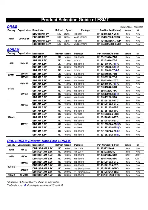
DRAMUpdated Date : 11/06/2006DensityOrganization DescriptionRefreshSpeedPackagePart Number(Pb-free)Sample MP EDO DRAM 5V 51225ns 40L-SOJ M11B416256A-25JP Now Now EDO DRAM 5V 51235ns 44-40L-TSOPII M11B416256A-35TG Now Now EDO DRAM 3.3V 51235ns 40L-SOJ M11L416256SA-35JP Now Now EDO DRAM 3.3V 51235ns 40/44L-TSOPIIM11L416256SA-35TGNowNowSDRAMDensityOrganization DescriptionRefresh SpeedPackagePart Number(Pb-free)Sample MP SDRAM 2.5V 2K 143MHz 50L-TSOPII M12S16161A-7TG Now Now SDRAM 2.5V 2K 143MHz VFBGA M12S16161A-7BG Now Now SDRAM 3.3V 2K 143MHz 50L-TSOPII M12L16161A-7T (I)G Now Now SDRAM 3.3V 2K 200MHz 50L-TSOPII M12L16161A-5T (I)G Now Now SDRAM 3.3V 2K 143MHz VFBGA M12L16161A-7B (I)G Now Now 2M*16SDRAM 3.3V 2K 143MHz 54L-TSOPII M12L32162A-7TG Now Now 1M*32SDRAM 3.3V 2K 143MHz 90-FBGA M12L32321A-7BG Now Now SDRAM 2.5V 4K 100MHz 54L-TSOPII M12S64164A-10TG Now Now SDRAM 3.3V 4K 143MHz 54L-TSOPII M12L64164A-7T (I)G Now Now SDRAM 3.3V 4K 200MHz 54L-TSOPII M12L64164A-5TG Now Now SDRAM 2.5V 4K 143MHz 86L-TSOPII M12S64322A-7TG Now Now SDRAM 3.3V 4K 166MHz 86L-TSOPII M12L64322A-6T (I)G Now Now SDRAM 3.3V 4K 200MHz 86L-TSOPII M12L64322A-5TG Now Now SDRAM 2.5V 4K 143MHz 54L-TSOPII M12S128168A-7TG Now Now SDRAM 2.5V 4K 166MHz 54L-TSOPII M12S128168A-6TG Now Now SDRAM 3.3V 4K 143MHz 54L-TSOPII M12L128168A-7TG Now Now SDRAM 3.3V 4K 166MHz 54L-TSOPII M12L128168A-6TG Now Now SDRAM 2.5V 4K 166MHz 90-FBGA M12S128324A-6BG Now Now SDRAM 2.5V 4K 143MHz 86L-TSOPII M12S128324A-7TG Now Now SDRAM 2.5V 4K 166MHz 86L-TSOPII M12S128324A-6TG Now Now SDRAM 3.3V 4K 143MHz 90-FBGA M12L128324A-7B (I)G Now Now SDRAM 3.3V 4K 166MHz 90-FBGA M12L128324A-6B (I)G Now Now SDRAM 3.3V 4K 143MHz 86L-TSOPII M12L128324A-7T (I)G Now Now SDRAM 3.3V4K166MHz86L-TSOPIIM12L128324A-6T (I)GNowNowDDR SDRAM (Dobule-Date-Rate SDRAM)Density Organization DescriptionRefresh SpeedPackagePart Number(Pb-free)Sample MP DDR-SDRAM 2.5V 4K 166MHz 100-LQFP M13S32321A-6L Now Now DDR-SDRAM 2.5V 4K 200MHz 100-LQFP M13S32321A-5L Now Now DDR-SDRAM 2.5V 4K 166MHz 66L-TSOPII M13S64164A-6TG Q2'07Q3'07DDR-SDRAM 2.5V 4K 200MHz 66L-TSOPII M13S64164A-5TG Q2'07Q3'07DDR-SDRAM 2.5V 4K 166MHz 66L-TSOPII M13S128168A-6TG Now Now DDR-SDRAM 2.5V 4K 200MHz 66L-TSOPII M13S128168A-5TG Now Now DDR-SDRAM 2.5V 4K 166MHz 144-FBGA (12x12mm)M13S128324A-6BG Now Now DDR-SDRAM 2.5V 4K 200MHz 144-FBGA (12x12mm)M13S128324A-5BG Now Now 256Mb16Mx16DDR-SDRAM 2.5V 4K200MHz66L-TSOPIIM13S2561616A-5TGNowNow*Identifier of Pb-free as G or P is shown on outer carton.**Industrial spec : (I) Operating temperature -40ºC ~+85 ºC.2M*3264Mb4Mb*1632Mb4Mb 256Kb*161Mb*1616Mb 128Mb8M*164Mx324M*32128Mb8M*1632Mb 64Mb1M*324M*16Mobile SDRAMDensityOrganizationDescriptionRefresh Speed Package & MCPPart Number(Pb-free)Sample MP Mobile SDRAM 2.5V4K 100MHz 50L-TSOPII M52S16161A-10T (I)G Now Now Mobile SDRAM 2.5V 4K 125MHz 50L-TSOPII M52S16161A-8T (I)G Now Now Mobile SDRAM 1.8V4K 100MHz50L-TSOPIIM52D16161A-10T (I)G Now Now Mobile SDRAM 2.5V 4K 100MHz 54L-TSOPII M52S32162A-10T (I)G Now Now Mobile SDRAM 2.5V 4K 100MHz 54-FBGA M52S32162A-10B (I)G Now Now Mobile SDRAM 2.5V 4K 133MHz 54L-TSOPII M52S32162A-7.5T (I)G Now Now Mobile SDRAM 2.5V 4K 133MHz 54-FBGA M52S32162A-7.5B (I)G Now Now Mobile SDRAM 1.8V 4K 100MHz 54L-TSOPII M52D32162A-10T (I)G Now Now Mobile SDRAM 1.8V 4K 100MHz 54-FBGA M52D32162A-10B (I)G Now Now Mobile SDRAM 1.8V 4K 100MHz 54L-TSOPII M52D32162A-7.5T (I)G Now Now Mobile SDRAM 1.8V 4K 133MHz 54-FBGA M52D32162A-7.5B (I)G Now Now Mobile SDRAM 2.5V 4K 100MHz 90-FBGA M52S32321A-10B (I)G Now Now Mobile SDRAM 2.5V 4K 133MHz 90-FBGA M52S32321A-7.5B (I)G Now Now Mobile SDRAM 1.8V 4K 100MHz 90-FBGA M52D32321A-10B (I)G Now Now Mobile SDRAM 1.8V 4K 133MHz 90-FBGA M52D32321A-7.5B (I)G Now Now Mobile SDRAM 2.5V 4K 100MHz 54L-TSOPII M52S64164A-10T (I)G Q2 '07Q3 '07Mobile SDRAM 2.5V 4K 100MHz 54-FBGA M52S64164A-10B (I)G Q2 '07Q3 '07Mobile SDRAM 2.5V 4K 133MHz 54L-TSOPII M52S64164A-7.5T (I)G Q2 '07Q3 '07Mobile SDRAM 2.5V 4K 133MHz 54-FBGA M52S64164A-7.5B (I)G Q2 '07Q3 '07Mobile SDRAM 1.8V 4K 100MHz 54L-TSOPII M52D64164A-10T (I)G Q2 '07Q3 '07Mobile SDRAM 1.8V 4K 100MHz 54-FBGA M52D64164A-10B (I)G Q2 '07Q3 '07Mobile SDRAM 1.8V 4K 100MHz 54L-TSOPII M52D64164A-7.5T (I)G Q2 '07Q3 '07Mobile SDRAM 1.8V 4K 133MHz 54-FBGA M52D64164A-7.5B (I)G Q2 '07Q3 '07Mobile SDRAM 2.5V 4K 100MHz 86L-TSOPII M52S64322A-10T (I)G Q2 '07Q3 '07Mobile SDRAM 2.5V 4K 100MHz 90-FBGA M52S64322A-10B (I)G Q2 '07Q3 '07Mobile SDRAM 2.5V 4K 133MHz 86L-TSOPII M52S64322A-7.5T (I)G Q2 '07Q3 '07Mobile SDRAM 2.5V 4K 133MHz 90-FBGA M52S64322A-7.5B (I)G Q2 '07Q3 '07Mobile SDRAM 1.8V 4K 100MHz 86L-TSOPII M52D64322A-10T (I)G Q2 '07Q3 '07Mobile SDRAM 1.8V 4K 100MHz 90-FBGA M52D64322A-10B (I)G Q2 '07Q3 '07Mobile SDRAM 1.8V 4K 100MHz 86L-TSOPII M52D64322A-7.5T (I)G Q2 '07Q3 '07Mobile SDRAM 1.8V4K133MHz 90-FBGAM52D64322A-7.5B (I)GQ2 '07Q3 '07*Identifier of Pb-free as G or P is shown on outer carton.**Industrial spec : (I) Operating temperature -40ºC ~+85 ºC.64Mb4Mx162Mx32(1)All Mobile functions are included : PASR,TCSR,DS,Deep power down mode.(2)Max. Icc6 : Self-refresh current with full bank in 70 ºC .1Mx16Max. Icc6= 75uA (1.8V)16Mb32Mb2Mx161Mx32。
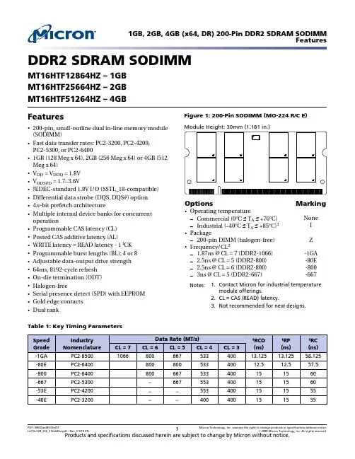
DDR2 SDRAM SODIMM MT16HTF12864HZ – 1GBMT16HTF25664HZ – 2GBMT16HTF51264HZ – 4GBFeatures•200-pin, small-outline dual in-line memory module (SODIMM)•Fast data transfer rates: PC2-3200, PC2-4200,PC2-5300, or PC2-6400•1GB (128 Meg x 64), 2GB (256 Meg x 64) or 4GB (512 Meg x 64)•V DD = V DDQ = 1.8V•V DDSPD = 1.7–3.6V•JEDEC-standard 1.8V I/O (SSTL_18-compatible)•Differential data strobe (DQS, DQS#) option•4n-bit prefetch architecture•Multiple internal device banks for concurrent operation•Programmable CAS latency (CL)•Posted CAS additive latency (AL)•WRITE latency = READ latency - 1 t CK •Programmable burst lengths (BL): 4 or 8•Adjustable data-output drive strength•64ms, 8192-cycle refresh•On-die termination (ODT)•Halogen-free•Serial presence detect (SPD) with EEPROM•Gold edge contacts•Dual rankFigure 1: 200-Pin SODIMM (MO-224 R/C E) Options Marking •Operating temperature–Commercial (0°C ≤ T A≤ +70°C)None–Industrial (–40°C ≤ T A≤ +85°C)1I •Package–200-pin DIMM (halogen-free)Z •Frequency/CL2– 1.87ns @ CL = 7 (DDR2-1066)-1GA– 2.5ns @ CL = 5 (DDR2-800)-80E– 2.5ns @ CL = 6 (DDR2-800)-800–3ns @ CL = 5 (DDR2-667)-667 Notes: 1.Contact Micron for industrial temperaturemodule offerings.2.CL = CAS (READ) latency.3.Not recommended for new designs.Table 1: Key Timing ParametersTable 2: AddressingTable 3: Part Numbers and Timing Parameters – 1GB Modules1Table 4: Part Numbers and Timing Parameters – 2GB Modules1Table 5: Part Numbers and Timing Parameters – 2GB Modules1Notes: 1.The data sheet for the base device can be found on Micron’s Web site.2.All part numbers end with a two-place code (not shown) that designates component and PCB revisions.Consult factory for current revision codes. Example: MT16HTF25664HZ-80EH1.Pin AssignmentsTable 6: Pin AssignmentsNotes: 1.Pin 85 is NC for 1GB and BA2 for 2GB, 4GB.2.Pin 86 is NC for 1GB, 2GB and A14 for 4GB.Pin DescriptionsThe pin description table below is a comprehensive list of all possible pins for all DDR2modules. All pins listed may not be supported on this module. See Pin Assignments forinformation specific to this module.Table 7: Pin DescriptionsTable 7: Pin Descriptions (Continued)Functional Block Diagram – 1GB, 2GB Figure 2: Functional Block Diagram – 1GB, 2GBCK0CK1VVVVBA[2/1:0]A[13:0]RAS#ODT1Rank 0 = U1, U2, U4–U9Rank 1 = U10, U11, U13–U18Functional Block Diagram – 4GB Figure 3: Functional Block Diagram – 4GBCK0CK1VVVVBA[2:0]A[14:0]RAS#ODT1Rank 0 = U1, U2, U5–U10Rank 1 = U11–U18General DescriptionDDR2 SDRAM modules are high-speed, CMOS dynamic random access memory mod-ules that use internally configured 4 or 8-bank DDR2 SDRAM devices. DDR2 SDRAMmodules use DDR architecture to achieve high-speed operation. DDR2 architecture isessentially a 4n-prefetch architecture with an interface designed to transfer two datawords per clock cycle at the I/O pins. A single read or write access for the DDR2 SDRAMmodule effectively consists of a single 4n-bit-wide, one-clock-cycle data transfer at theinternal DRAM core and eight corresponding n-bit-wide, one-half-clock-cycle data trans-fers at the I/O pins.DDR2 modules use two sets of differential signals: DQS, DQS# to capture data and CKand CK# to capture commands, addresses, and control signals. Differential clocks anddata strobes ensure exceptional noise immunity for these signals and provide precisecrossing points to capture input signals. A bidirectional data strobe (DQS, DQS#) is trans-mitted externally, along with data, for use in data capture at the receiver. DQS is astrobe transmitted by the DDR2 SDRAM device during READs and by the memory con-troller during WRITEs. DQS is edge-aligned with data for READs and center-alignedwith data for WRITEs.DDR2 SDRAM modules operate from a differential clock (CK and CK#); the crossing ofCK going HIGH and CK# going LOW will be referred to as the positive edge of CK. Com-mands (address and control signals) are registered at every positive edge of CK. Inputdata is registered on both edges of DQS, and output data is referenced to both edges ofDQS, as well as to both edges of CK.Serial Presence-Detect EEPROM OperationDDR2 SDRAM modules incorporate serial presence-detect. The SPD data is stored in a256-byte EEPROM. The first 128 bytes are programmed by Micron to identify the mod-ule type and various SDRAM organizations and timing parameters. The remaining 128bytes of storage are available for use by the customer. System READ/WRITE operationsbetween the master (system logic) and the slave EEPROM device occur via a standardI2C bus using the DIMM’s SCL (clock) SDA (data), and SA (address) pins. Write protect(WP) is connected to V SS, permanently disabling hardware write protection.Electrical SpecificationsStresses greater than those listed may cause permanent damage to the module. This is astress rating only, and functional operation of the module at these or any other condi-tions outside those indicated in the device data sheet are not implied. Exposure toabsolute maximum rating conditions for extended periods may adversely affect reliability. Table 8: Absolute Maximum RatingsNotes: 1.The refresh rate is required to double when T C exceeds 85°C.2.For further information, refer to technical note TN-00-08: "Thermal Applications," avail-able on Micron’s Web site.DRAM Operating ConditionsRecommended AC operating conditions are given in the DDR2 component data ponent specifications are available on Micron's Web site. Module speed grades cor-relate with component speed grades.Table 9: Module and Component Speed GradesDesign ConsiderationsSimulationsMicron memory modules are designed to optimize signal integrity through carefully de-signed terminations, controlled board impedances, routing topologies, trace lengthmatching, and decoupling. However, good signal integrity starts at the system level. Mi-cron encourages designers to simulate the signal characteristics of the system's memo-ry bus to ensure adequate signal integrity of the entire memory system.PowerOperating voltages are specified at the DRAM, not at the edge connector of the module.Designers must account for any system voltage drops at anticipated power levels to en-sure the required supply voltage is maintained.1GB, 2GB, 4GB (x64, DR) 200-Pin DDR2 SDRAM SODIMMDRAM Operating ConditionsIDD SpecificationsTable 10: DDR2 I DD Specifications and Conditions – 1GBValues shown for MT47H64M8 DDR2 SDRAM only and are computed from values specified in the 512Mb (64 Meg x 8)Table 10: DDR2 I DD Specifications and Conditions – 1GB (Continued)Values shown for MT47H64M8 DDR2 SDRAM only and are computed from values specified in the 512Mb (64 Meg x 8)Notes: 1.Value calculated as one module rank in this operating condition; all other module ranksin I DD2P (CKE LOW) mode.2.Value calculated reflects all module ranks in this operating condition.Table 11: DDR2 I DD Specifications and Conditions – 2GB (Die Revision E and G)Values shown for MT47H128M8 DDR2 SDRAM only and are computed from values specified in the 1Gb (128 Meg x 8) com-Table 11: DDR2 I DD Specifications and Conditions – 2GB (Die Revision E and G) (Continued)Values shown for MT47H128M8 DDR2 SDRAM only and are computed from values specified in the 1Gb (128 Meg x 8) com-Notes: 1.Value calculated as one module rank in this operating condition; all other module ranksin I DD2P (CKE LOW) mode.2.Value calculated reflects all module ranks in this operating condition.Table 12: DDR2 I DD Specifications and Conditions – 2GB (Die Revision H)Values shown for MT47H128M8 DDR2 SDRAM only and are computed from values specified in the 1Gb (128 Meg x 8) com-Table 12: DDR2 I DD Specifications and Conditions – 2GB (Die Revision H) (Continued)Values shown for MT47H128M8 DDR2 SDRAM only and are computed from values specified in the 1Gb (128 Meg x 8) com-Notes:1.Value calculated as one module rank in this operating condition; all other module ranksin I DD2P (CKE LOW) mode.2.Value calculated reflects all module ranks in this operating condition.Table 13: DDR2 I DD Specifications and Conditions – 4GB (Die Revision A)Values shown for MT47H256M8 DDR2 SDRAM only and are computed from values specified in the 2Gb (256 Meg x 8) com-Table 13: DDR2 I DD Specifications and Conditions – 4GB (Die Revision A) (Continued)Values shown for MT47H256M8 DDR2 SDRAM only and are computed from values specified in the 2Gb (256 Meg x 8) com-Notes: 1.Value calculated as one module rank in this operating condition; all other module ranksin I DD2P (CKE LOW) mode.2.Value calculated reflects all module ranks in this operating condition.Serial Presence-DetectFor the latest SPD data, refer to Micron's SPD page: /SPD .Table 14: SPD EEPROM Operating ConditionsTable 15: SPD EEPROM AC Operating ConditionsNotes:1.To avoid spurious start and stop conditions, a minimum delay is placed between SCL = 1and the falling or rising edge of SDA.2.This parameter is sampled.3.For a restart condition or following a WRITE cycle.4.The SPD EEPROM WRITE cycle time (t WRC) is the time from a valid stop condition of awrite sequence to the end of the EEPROM internal ERASE/PROGRAM cycle. During the WRITE cycle, the EEPROM bus interface circuit is disabled, SDA remains HIGH due to pull-up resistance, and the EEPROM does not respond to its slave address.1GB, 2GB, 4GB (x64, DR) 200-Pin DDR2 SDRAM SODIMMSerial Presence-DetectModule Dimensions – 1GB, 2GBFigure 4: 200-Pin DDR2 SODIMM – 1GB, 2GB3.8 (0.15) Front viewTYPNotes:1.All dimensions are in millimeters (inches); MAX/MIN or typical (TYP) where noted.2.The dimensional diagram is for reference only. Refer to the JEDEC MO document foradditional design dimensions.Module Dimensions – 4GBFigure 5: 200-Pin DDR2 SODIMM – 4GBTYPNotes: 1.All dimensions are in millimeters (inches); MAX/MIN or typical (TYP) where noted.2.The dimensional diagram is for reference only. Refer to the JEDEC MO document foradditional design dimensions.8000 S. Federal Way, P.O. Box 6, Boise, ID 83707-0006, Tel: 208-368-3900/productsupport Customer Comment Line: 800-932-4992Micron and the Micron logo are trademarks of Micron Technology, Inc.All other trademarks are the property of their respective owners.This data sheet contains minimum and maximum limits specified over the power supply and temperature range set forth herein. Although considered final, these specifications are subject to change, as further product development and data characterization some-times occur.。
Important Notes and WarningsMicron Technology, Inc. ("Micron") reserves the right to make changes to information published in this document, including without limitation specifications and product descriptions. This document supersedes and replaces all information supplied prior to the publication hereof. You may not rely on any information set forth in this docu-ment if you obtain the product described herein from any unauthorized distributor or other source not authorized by Micron.Automotive Applications. Products are not designed or intended for use in automotive applications unless specifi-cally designated by Micron as automotive-grade by their respective data sheets. Distributor and customer/distrib-utor shall assume the sole risk and liability for and shall indemnify and hold Micron harmless against all claims, costs, damages, and expenses and reasonable attorneys' fees arising out of, directly or indirectly, any claim of product liability, personal injury, death, or property damage resulting directly or indirectly from any use of non-automotive-grade products in automotive applications. Customer/distributor shall ensure that the terms and con-ditions of sale between customer/distributor and any customer of distributor/customer (1) state that Micron products are not designed or intended for use in automotive applications unless specifically designated by Micron as automotive-grade by their respective data sheets and (2) require such customer of distributor/customer to in-demnify and hold Micron harmless against all claims, costs, damages, and expenses and reasonable attorneys' fees arising out of, directly or indirectly, any claim of product liability, personal injury, death, or property damage resulting from any use of non-automotive-grade products in automotive applications.Critical Applications. Products are not authorized for use in applications in which failure of the Micron compo-nent could result, directly or indirectly in death, personal injury, or severe property or environmental damage ("Critical Applications"). Customer must protect against death, personal injury, and severe property and environ-mental damage by incorporating safety design measures into customer's applications to ensure that failure of the Micron component will not result in such harms. Should customer or distributor purchase, use, or sell any Micron component for any critical application, customer and distributor shall indemnify and hold harmless Micron and its subsidiaries, subcontractors, and affiliates and the directors, officers, and employees of each against all claims, costs, damages, and expenses and reasonable attorneys' fees arising out of, directly or indirectly, any claim of product liability, personal injury, or death arising in any way out of such critical application, whether or not Mi-cron or its subsidiaries, subcontractors, or affiliates were negligent in the design, manufacture, or warning of the Micron product.Customer Responsibility. Customers are responsible for the design, manufacture, and operation of their systems, applications, and products using Micron products. ALL SEMICONDUCTOR PRODUCTS HAVE INHERENT FAIL-URE RATES AND LIMITED USEFUL LIVES. IT IS THE CUSTOMER'S SOLE RESPONSIBILITY TO DETERMINE WHETHER THE MICRON PRODUCT IS SUITABLE AND FIT FOR THE CUSTOMER'S SYSTEM, APPLICATION, OR PRODUCT. Customers must ensure that adequate design, manufacturing, and operating safeguards are included in customer's applications and products to eliminate the risk that personal injury, death, or severe property or en-vironmental damages will result from failure of any semiconductor component.Limited Warranty. In no event shall Micron be liable for any indirect, incidental, punitive, special or consequential damages (including without limitation lost profits, lost savings, business interruption, costs related to the removal or replacement of any products or rework charges) whether or not such damages are based on tort, warranty, breach of contract or other legal theory, unless explicitly stated in a written agreement executed by Micron's duly authorized representative.质量等级领域:宇航级IC、特军级IC、超军级IC、普军级IC、禁运IC、工业级IC,军级二三极管,功率管等;应用领域:航空航天、船舶、汽车电子、军用计算机、铁路、医疗电子、通信网络、电力工业以及大型工业设备祝您:工作顺利,生活愉快!以深圳市美光存储技术有限公司提供的参数为例,以下为MTA18ASF2G72PZ-2G6D1的详细参数,仅供参考I DD SpecificationsTable 5: DDR4 I DD Specifications and Conditions (0° ≤ T C≤ 85°) – 16GB (Die Revision B)Values are for the MT40A2G4 DDR4 SDRAM only and are computed from values specified in the 8Gb (2 Gig x 4) compo-nent data sheetTable 6: DDR4 I DD Specifications and Conditions (0° ≤ T C≤ 85°) – 16GB (Die Revision D)Values are for the MT40A2G4 DDR4 SDRAM only and are computed from values specified in the 8Gb (2 Gig x 4) compo-nent data sheetTable 7: DDR4 I DD Specifications and Conditions (0° ≤ T C≤ 85°) – 16GB (Die Revision E)Values are for the MT40A2G4 DDR4 SDRAM only and are computed from values specified in the 8Gb (2 Gig x 4) compo-Note: 1.When T C > 85°C, the I DD and I PP values must be derated. Refer to the base device datasheet I DD and I PP specification tables for derating values for the applicable die-revision.Table 8: DDR4 I DD Specifications and Conditions (0° ≤ T C≤ 85°) – 16GB (Die Revision J)Values are for the MT40A2G4 DDR4 SDRAM only and are computed from values specified in the 8Gb (2 Gig x 4) compo-Note: 1.When T C > 85°C, the I DD and I PP values must be derated. Refer to the base device datasheet I DD and I PP specification tables for derating values for the applicable die-revision.。
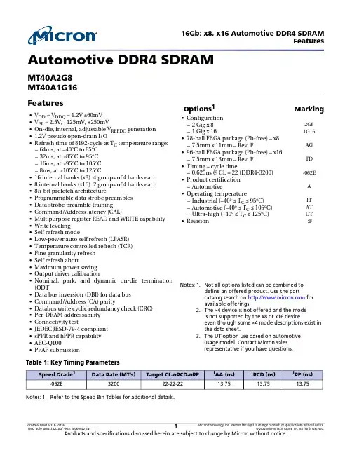
Automotive DDR4 SDRAM MT40A2G8MT40A1G16FeaturesNotes:1.Not all options listed can be combined to define an offered product. Use the part catalog search on for available offerings.2.The ×4 device is not offered and the mode is not supported by the x8 or x16 device even tho ugh some ×4 mode descriptions exist in the data sheet.3.The UT option use based on automotive usage model. Contact Micron sales representative if you have questions.Notes:1.Refer to the Speed Bin Tables for additional details.•V DD = V DDQ = 1.2V ±60mV •V PP = 2.5V, –125mV, +250mV •On-die, internal, adjustable V REFDQ generation •1.2V pseudo open-drain I/O •Refresh time of 8192-cycle at T C temperature range:–64ms, at –40°C to 85°C–32ms, at >85°C to 95°C–16ms, at >95°C to 105°C–8ms, at >105°C to 125°C•16 internal banks (x8): 4 groups of 4 banks each•8 internal banks (x16): 2 groups of 4 banks each•8n -bit prefetch architecture•Programmable data strobe preambles•Data strobe preamble training•Command/Address latency (CAL)•Multipurpose register READ and WRITE capability•Write leveling•Self refresh mode•Low-power auto self refresh (LPASR)•Temperature controlled refresh (TCR)•Fine granularity refresh•Self refresh abort•Maximum power saving•Output driver calibration•Nominal, park, and dynamic on-die termination(ODT)•Data bus inversion (DBI) for data bus•Command/Address (CA) parity•Databus write cyclic redundancy check (CRC)•Per-DRAM addressability•Connectivity test•JEDEC JESD-79-4 compliant•sPPR and hPPR capability•AEC-Q100•PPAP submission Options 1Marking •Configuration –2 Gig x 82G8–1 Gig x 161G16•78-ball FBGA package (Pb-free) – x8–7.5mm x 11mm – Rev. F AG •96-ball FBGA package (Pb-free) – x16–7.5mm x 13mm – Rev. F TD •Timing – cycle time –0.625ns @ CL = 22 (DDR4-3200)-062E •Product certification –Automotive A •Operating temperature –Industrial (–40° ≤ T C ≤ 95°C)IT –Automotive (–40° ≤ T C ≤ 105°C)AT –Ultra-high (–40° ≤ T C ≤ 125°C)UT •Revision :F Table 1: Key Timing Parameters Speed Grade 1Data Rate (MT/s)Target CL-n RCD-n RP t AA (ns)t RCD (ns)t RP (ns)-062E 320022-22-2213.7513.7513.75Table 2: AddressingParameter2048 Meg x 81024 Meg x 16 Number of bank groups42Bank group address BG[1:0]BG0Bank count per group44Bank address in bank group BA[1:0]BA[1:0]Row addressing 128K (A[16:0])128K (A[16:0])Column addressing 1K (A[9:0]) 1K (A[9:0])Page size11KB2KBNotes:1.Page size is per bank, calculated as follows:Page size = 2COLBITS× ORG/8, where COLBIT = the number of column address bits and ORG = the number of DQ bits. Figure 1: Order Part Number ExampleExample Part Number: MT40A1G16KH-062E AAT:EContentsImportant Notes and Warnings . . . . . . . . . . . . . . . . . . . . . . . . . . . . . . . . . . . . . . . . . . . . . . . . . . . . . . . . . . . . . . . . . . . . . . . . . 18 General Notes and Description . . . . . . . . . . . . . . . . . . . . . . . . . . . . . . . . . . . . . . . . . . . . . . . . . . . . . . . . . . . . . . . . . . . . . . . . . . 19 Description . . . . . . . . . . . . . . . . . . . . . . . . . . . . . . . . . . . . . . . . . . . . . . . . . . . . . . . . . . . . . . . . . . . . . . . . . . . . . . . . . . . . . . . . . 19 Industrial Temperature . . . . . . . . . . . . . . . . . . . . . . . . . . . . . . . . . . . . . . . . . . . . . . . . . . . . . . . . . . . . . . . . . . . . . . . . . . . . . . 19 Automotive Temperature . . . . . . . . . . . . . . . . . . . . . . . . . . . . . . . . . . . . . . . . . . . . . . . . . . . . . . . . . . . . . . . . . . . . . . . . . . . . 19 Ultra-high Temperature . . . . . . . . . . . . . . . . . . . . . . . . . . . . . . . . . . . . . . . . . . . . . . . . . . . . . . . . . . . . . . . . . . . . . . . . . . . . . . 19 General Notes . . . . . . . . . . . . . . . . . . . . . . . . . . . . . . . . . . . . . . . . . . . . . . . . . . . . . . . . . . . . . . . . . . . . . . . . . . . . . . . . . . . . . . . 19 Definitions of the Device-Pin Signal Level . . . . . . . . . . . . . . . . . . . . . . . . . . . . . . . . . . . . . . . . . . . . . . . . . . . . . . . . . . . . . . 20 Definitions of the Bus Signal Level . . . . . . . . . . . . . . . . . . . . . . . . . . . . . . . . . . . . . . . . . . . . . . . . . . . . . . . . . . . . . . . . . . . . 20 Functional Block Diagrams . . . . . . . . . . . . . . . . . . . . . . . . . . . . . . . . . . . . . . . . . . . . . . . . . . . . . . . . . . . . . . . . . . . . . . . . . . . . . 21 Ball Assignments . . . . . . . . . . . . . . . . . . . . . . . . . . . . . . . . . . . . . . . . . . . . . . . . . . . . . . . . . . . . . . . . . . . . . . . . . . . . . . . . . . . . . . 22 Ball Descriptions . . . . . . . . . . . . . . . . . . . . . . . . . . . . . . . . . . . . . . . . . . . . . . . . . . . . . . . . . . . . . . . . . . . . . . . . . . . . . . . . . . . . . . 24 Package Dimensions . . . . . . . . . . . . . . . . . . . . . . . . . . . . . . . . . . . . . . . . . . . . . . . . . . . . . . . . . . . . . . . . . . . . . . . . . . . . . . . . . . . 27 State Diagram . . . . . . . . . . . . . . . . . . . . . . . . . . . . . . . . . . . . . . . . . . . . . . . . . . . . . . . . . . . . . . . . . . . . . . . . . . . . . . . . . . . . . . . . . 29 Functional Description . . . . . . . . . . . . . . . . . . . . . . . . . . . . . . . . . . . . . . . . . . . . . . . . . . . . . . . . . . . . . . . . . . . . . . . . . . . . . . . . . 31 RESET and Initialization Procedure . . . . . . . . . . . . . . . . . . . . . . . . . . . . . . . . . . . . . . . . . . . . . . . . . . . . . . . . . . . . . . . . . . . . . . 32 Power-Up and Initialization Sequence . . . . . . . . . . . . . . . . . . . . . . . . . . . . . . . . . . . . . . . . . . . . . . . . . . . . . . . . . . . . . . . . . 32 RESET Initialization with Stable Power Sequence . . . . . . . . . . . . . . . . . . . . . . . . . . . . . . . . . . . . . . . . . . . . . . . . . . . . . . . 35 Uncontrolled Power-Down Sequence . . . . . . . . . . . . . . . . . . . . . . . . . . . . . . . . . . . . . . . . . . . . . . . . . . . . . . . . . . . . . . . . . 36 Programming Mode Registers . . . . . . . . . . . . . . . . . . . . . . . . . . . . . . . . . . . . . . . . . . . . . . . . . . . . . . . . . . . . . . . . . . . . . . . . . . . 36 Mode Register 0 . . . . . . . . . . . . . . . . . . . . . . . . . . . . . . . . . . . . . . . . . . . . . . . . . . . . . . . . . . . . . . . . . . . . . . . . . . . . . . . . . . . . . . . 39 Burst Length, Type, and Order . . . . . . . . . . . . . . . . . . . . . . . . . . . . . . . . . . . . . . . . . . . . . . . . . . . . . . . . . . . . . . . . . . . . . . . . 40 CAS Latency . . . . . . . . . . . . . . . . . . . . . . . . . . . . . . . . . . . . . . . . . . . . . . . . . . . . . . . . . . . . . . . . . . . . . . . . . . . . . . . . . . . . . . . . 41 Test Mode . . . . . . . . . . . . . . . . . . . . . . . . . . . . . . . . . . . . . . . . . . . . . . . . . . . . . . . . . . . . . . . . . . . . . . . . . . . . . . . . . . . . . . . . . . 42 Write Recovery (WR)/READ-to-PRECHARGE . . . . . . . . . . . . . . . . . . . . . . . . . . . . . . . . . . . . . . . . . . . . . . . . . . . . . . . . . . . 42 DLL RESET . . . . . . . . . . . . . . . . . . . . . . . . . . . . . . . . . . . . . . . . . . . . . . . . . . . . . . . . . . . . . . . . . . . . . . . . . . . . . . . . . . . . . . . . . 42 Mode Register 1 . . . . . . . . . . . . . . . . . . . . . . . . . . . . . . . . . . . . . . . . . . . . . . . . . . . . . . . . . . . . . . . . . . . . . . . . . . . . . . . . . . . . . . . 43 DLL Enable/DLL Disable . . . . . . . . . . . . . . . . . . . . . . . . . . . . . . . . . . . . . . . . . . . . . . . . . . . . . . . . . . . . . . . . . . . . . . . . . . . . . 44 Output Driver Impedance Control . . . . . . . . . . . . . . . . . . . . . . . . . . . . . . . . . . . . . . . . . . . . . . . . . . . . . . . . . . . . . . . . . . . . 45 ODT R TT(NOM) Values . . . . . . . . . . . . . . . . . . . . . . . . . . . . . . . . . . . . . . . . . . . . . . . . . . . . . . . . . . . . . . . . . . . . . . . . . . . . . . . . 45 Additive Latency . . . . . . . . . . . . . . . . . . . . . . . . . . . . . . . . . . . . . . . . . . . . . . . . . . . . . . . . . . . . . . . . . . . . . . . . . . . . . . . . . . . . 45 Rx CTLE Control . . . . . . . . . . . . . . . . . . . . . . . . . . . . . . . . . . . . . . . . . . . . . . . . . . . . . . . . . . . . . . . . . . . . . . . . . . . . . . . . . . . . . 45 Write Leveling . . . . . . . . . . . . . . . . . . . . . . . . . . . . . . . . . . . . . . . . . . . . . . . . . . . . . . . . . . . . . . . . . . . . . . . . . . . . . . . . . . . . . . . 45 Output Disable . . . . . . . . . . . . . . . . . . . . . . . . . . . . . . . . . . . . . . . . . . . . . . . . . . . . . . . . . . . . . . . . . . . . . . . . . . . . . . . . . . . . . . 45 Termination Data Strobe . . . . . . . . . . . . . . . . . . . . . . . . . . . . . . . . . . . . . . . . . . . . . . . . . . . . . . . . . . . . . . . . . . . . . . . . . . . . . 46 Mode Register 2 . . . . . . . . . . . . . . . . . . . . . . . . . . . . . . . . . . . . . . . . . . . . . . . . . . . . . . . . . . . . . . . . . . . . . . . . . . . . . . . . . . . . . . . 47 CAS WRITE Latency . . . . . . . . . . . . . . . . . . . . . . . . . . . . . . . . . . . . . . . . . . . . . . . . . . . . . . . . . . . . . . . . . . . . . . . . . . . . . . . . . 48 Low-Power Auto Self Refresh . . . . . . . . . . . . . . . . . . . . . . . . . . . . . . . . . . . . . . . . . . . . . . . . . . . . . . . . . . . . . . . . . . . . . . . . . 48 Dynamic ODT . . . . . . . . . . . . . . . . . . . . . . . . . . . . . . . . . . . . . . . . . . . . . . . . . . . . . . . . . . . . . . . . . . . . . . . . . . . . . . . . . . . . . . . 49 Write Cyclic Redundancy Check Data Bus . . . . . . . . . . . . . . . . . . . . . . . . . . . . . . . . . . . . . . . . . . . . . . . . . . . . . . . . . . . . . . 49 Mode Register 3 . . . . . . . . . . . . . . . . . . . . . . . . . . . . . . . . . . . . . . . . . . . . . . . . . . . . . . . . . . . . . . . . . . . . . . . . . . . . . . . . . . . . . . . 50 Multipurpose Register . . . . . . . . . . . . . . . . . . . . . . . . . . . . . . . . . . . . . . . . . . . . . . . . . . . . . . . . . . . . . . . . . . . . . . . . . . . . . . . 51 WRITE Command Latency When CRC/DM is Enabled . . . . . . . . . . . . . . . . . . . . . . . . . . . . . . . . . . . . . . . . . . . . . . . . . . 51 Fine Granularity Refresh Mode . . . . . . . . . . . . . . . . . . . . . . . . . . . . . . . . . . . . . . . . . . . . . . . . . . . . . . . . . . . . . . . . . . . . . . . 52 Temperature Sensor Status . . . . . . . . . . . . . . . . . . . . . . . . . . . . . . . . . . . . . . . . . . . . . . . . . . . . . . . . . . . . . . . . . . . . . . . . . . . 52 Per-DRAM Addressability . . . . . . . . . . . . . . . . . . . . . . . . . . . . . . . . . . . . . . . . . . . . . . . . . . . . . . . . . . . . . . . . . . . . . . . . . . . . 52 Gear-Down Mode . . . . . . . . . . . . . . . . . . . . . . . . . . . . . . . . . . . . . . . . . . . . . . . . . . . . . . . . . . . . . . . . . . . . . . . . . . . . . . . . . . . 52 Mode Register 4 . . . . . . . . . . . . . . . . . . . . . . . . . . . . . . . . . . . . . . . . . . . . . . . . . . . . . . . . . . . . . . . . . . . . . . . . . . . . . . . . . . . . . . . 53 Hard Post Package Repair Mode . . . . . . . . . . . . . . . . . . . . . . . . . . . . . . . . . . . . . . . . . . . . . . . . . . . . . . . . . . . . . . . . . . . . . . 54 Soft Post Package Repair Mode . . . . . . . . . . . . . . . . . . . . . . . . . . . . . . . . . . . . . . . . . . . . . . . . . . . . . . . . . . . . . . . . . . . . . . . 54 WRITE Preamble . . . . . . . . . . . . . . . . . . . . . . . . . . . . . . . . . . . . . . . . . . . . . . . . . . . . . . . . . . . . . . . . . . . . . . . . . . . . . . . . . . . . 55READ Preamble . . . . . . . . . . . . . . . . . . . . . . . . . . . . . . . . . . . . . . . . . . . . . . . . . . . . . . . . . . . . . . . . . . . . . . . . . . . . . . . . . . . . . 55 READ Preamble Training . . . . . . . . . . . . . . . . . . . . . . . . . . . . . . . . . . . . . . . . . . . . . . . . . . . . . . . . . . . . . . . . . . . . . . . . . . . . . 55 Temperature-Controlled Refresh . . . . . . . . . . . . . . . . . . . . . . . . . . . . . . . . . . . . . . . . . . . . . . . . . . . . . . . . . . . . . . . . . . . . . . 55 Command Address Latency . . . . . . . . . . . . . . . . . . . . . . . . . . . . . . . . . . . . . . . . . . . . . . . . . . . . . . . . . . . . . . . . . . . . . . . . . . 55 Internal V REF Monitor . . . . . . . . . . . . . . . . . . . . . . . . . . . . . . . . . . . . . . . . . . . . . . . . . . . . . . . . . . . . . . . . . . . . . . . . . . . . . . . . 55 Maximum Power Savings Mode . . . . . . . . . . . . . . . . . . . . . . . . . . . . . . . . . . . . . . . . . . . . . . . . . . . . . . . . . . . . . . . . . . . . . . . 55 Mode Register 5 . . . . . . . . . . . . . . . . . . . . . . . . . . . . . . . . . . . . . . . . . . . . . . . . . . . . . . . . . . . . . . . . . . . . . . . . . . . . . . . . . . . . . . . 56 Data Bus Inversion . . . . . . . . . . . . . . . . . . . . . . . . . . . . . . . . . . . . . . . . . . . . . . . . . . . . . . . . . . . . . . . . . . . . . . . . . . . . . . . . . . 57 Data Mask . . . . . . . . . . . . . . . . . . . . . . . . . . . . . . . . . . . . . . . . . . . . . . . . . . . . . . . . . . . . . . . . . . . . . . . . . . . . . . . . . . . . . . . . . . 57 CA Parity Persistent Error Mode . . . . . . . . . . . . . . . . . . . . . . . . . . . . . . . . . . . . . . . . . . . . . . . . . . . . . . . . . . . . . . . . . . . . . . . 58 ODT Input Buffer for Power-Down . . . . . . . . . . . . . . . . . . . . . . . . . . . . . . . . . . . . . . . . . . . . . . . . . . . . . . . . . . . . . . . . . . . . 58 CA Parity Error Status . . . . . . . . . . . . . . . . . . . . . . . . . . . . . . . . . . . . . . . . . . . . . . . . . . . . . . . . . . . . . . . . . . . . . . . . . . . . . . . . 58 CRC Error Status . . . . . . . . . . . . . . . . . . . . . . . . . . . . . . . . . . . . . . . . . . . . . . . . . . . . . . . . . . . . . . . . . . . . . . . . . . . . . . . . . . . . 58 CA Parity Latency Mode . . . . . . . . . . . . . . . . . . . . . . . . . . . . . . . . . . . . . . . . . . . . . . . . . . . . . . . . . . . . . . . . . . . . . . . . . . . . . . 58 Mode Register 6 . . . . . . . . . . . . . . . . . . . . . . . . . . . . . . . . . . . . . . . . . . . . . . . . . . . . . . . . . . . . . . . . . . . . . . . . . . . . . . . . . . . . . . . 59 Data Rate Programming . . . . . . . . . . . . . . . . . . . . . . . . . . . . . . . . . . . . . . . . . . . . . . . . . . . . . . . . . . . . . . . . . . . . . . . . . . . . . . 60 V REFDQ Calibration Enable . . . . . . . . . . . . . . . . . . . . . . . . . . . . . . . . . . . . . . . . . . . . . . . . . . . . . . . . . . . . . . . . . . . . . . . . . . . 60 V REFDQ Calibration Range . . . . . . . . . . . . . . . . . . . . . . . . . . . . . . . . . . . . . . . . . . . . . . . . . . . . . . . . . . . . . . . . . . . . . . . . . . . . 60 V REFDQ Calibration Value . . . . . . . . . . . . . . . . . . . . . . . . . . . . . . . . . . . . . . . . . . . . . . . . . . . . . . . . . . . . . . . . . . . . . . . . . . . . . 60 Truth Tables . . . . . . . . . . . . . . . . . . . . . . . . . . . . . . . . . . . . . . . . . . . . . . . . . . . . . . . . . . . . . . . . . . . . . . . . . . . . . . . . . . . . . . . . 61 NOP Command . . . . . . . . . . . . . . . . . . . . . . . . . . . . . . . . . . . . . . . . . . . . . . . . . . . . . . . . . . . . . . . . . . . . . . . . . . . . . . . . . . . . . . . 66 DESELECT Command . . . . . . . . . . . . . . . . . . . . . . . . . . . . . . . . . . . . . . . . . . . . . . . . . . . . . . . . . . . . . . . . . . . . . . . . . . . . . . . . . . 66 DLL-Off Mode . . . . . . . . . . . . . . . . . . . . . . . . . . . . . . . . . . . . . . . . . . . . . . . . . . . . . . . . . . . . . . . . . . . . . . . . . . . . . . . . . . . . . . . . . 66 DLL-On/Off Switching Procedures . . . . . . . . . . . . . . . . . . . . . . . . . . . . . . . . . . . . . . . . . . . . . . . . . . . . . . . . . . . . . . . . . . . . . . 68 DLL Switch Sequence from DLL-On to DLL-Off . . . . . . . . . . . . . . . . . . . . . . . . . . . . . . . . . . . . . . . . . . . . . . . . . . . . . . . . . 68 DLL-Off to DLL-On Procedure . . . . . . . . . . . . . . . . . . . . . . . . . . . . . . . . . . . . . . . . . . . . . . . . . . . . . . . . . . . . . . . . . . . . . . . . 70 Input Clock Frequency Change . . . . . . . . . . . . . . . . . . . . . . . . . . . . . . . . . . . . . . . . . . . . . . . . . . . . . . . . . . . . . . . . . . . . . . . . . . 71 Write Leveling . . . . . . . . . . . . . . . . . . . . . . . . . . . . . . . . . . . . . . . . . . . . . . . . . . . . . . . . . . . . . . . . . . . . . . . . . . . . . . . . . . . . . . . . . 71 DRAM Setting for Write Leveling and DRAM TERMINATION Function in that Mode . . . . . . . . . . . . . . . . . . . . . . . 73 Procedure Description . . . . . . . . . . . . . . . . . . . . . . . . . . . . . . . . . . . . . . . . . . . . . . . . . . . . . . . . . . . . . . . . . . . . . . . . . . . . . . . 73 Write Leveling Mode Exit . . . . . . . . . . . . . . . . . . . . . . . . . . . . . . . . . . . . . . . . . . . . . . . . . . . . . . . . . . . . . . . . . . . . . . . . . . . . . 75 Command Address Latency . . . . . . . . . . . . . . . . . . . . . . . . . . . . . . . . . . . . . . . . . . . . . . . . . . . . . . . . . . . . . . . . . . . . . . . . . . . . . 76 Low-Power Auto Self Refresh Mode . . . . . . . . . . . . . . . . . . . . . . . . . . . . . . . . . . . . . . . . . . . . . . . . . . . . . . . . . . . . . . . . . . . . . . 80 Manual Self Refresh Mode . . . . . . . . . . . . . . . . . . . . . . . . . . . . . . . . . . . . . . . . . . . . . . . . . . . . . . . . . . . . . . . . . . . . . . . . . . . . 80 Multipurpose Register . . . . . . . . . . . . . . . . . . . . . . . . . . . . . . . . . . . . . . . . . . . . . . . . . . . . . . . . . . . . . . . . . . . . . . . . . . . . . . . . . . 82 MPR Reads . . . . . . . . . . . . . . . . . . . . . . . . . . . . . . . . . . . . . . . . . . . . . . . . . . . . . . . . . . . . . . . . . . . . . . . . . . . . . . . . . . . . . . . . . 83 MPR Readout Format . . . . . . . . . . . . . . . . . . . . . . . . . . . . . . . . . . . . . . . . . . . . . . . . . . . . . . . . . . . . . . . . . . . . . . . . . . . . . . . . 85 MPR Readout Serial Format . . . . . . . . . . . . . . . . . . . . . . . . . . . . . . . . . . . . . . . . . . . . . . . . . . . . . . . . . . . . . . . . . . . . . . . . . . 85 MPR Readout Parallel Format . . . . . . . . . . . . . . . . . . . . . . . . . . . . . . . . . . . . . . . . . . . . . . . . . . . . . . . . . . . . . . . . . . . . . . . . . 86 MPR Readout Staggered Format . . . . . . . . . . . . . . . . . . . . . . . . . . . . . . . . . . . . . . . . . . . . . . . . . . . . . . . . . . . . . . . . . . . . . . 87 MPR READ Waveforms . . . . . . . . . . . . . . . . . . . . . . . . . . . . . . . . . . . . . . . . . . . . . . . . . . . . . . . . . . . . . . . . . . . . . . . . . . . . . . . 88 MPR Writes . . . . . . . . . . . . . . . . . . . . . . . . . . . . . . . . . . . . . . . . . . . . . . . . . . . . . . . . . . . . . . . . . . . . . . . . . . . . . . . . . . . . . . . . . 90 MPR WRITE Waveforms . . . . . . . . . . . . . . . . . . . . . . . . . . . . . . . . . . . . . . . . . . . . . . . . . . . . . . . . . . . . . . . . . . . . . . . . . . . . . . 90 MPR REFRESH Waveforms . . . . . . . . . . . . . . . . . . . . . . . . . . . . . . . . . . . . . . . . . . . . . . . . . . . . . . . . . . . . . . . . . . . . . . . . . . . 92 Gear-Down Mode . . . . . . . . . . . . . . . . . . . . . . . . . . . . . . . . . . . . . . . . . . . . . . . . . . . . . . . . . . . . . . . . . . . . . . . . . . . . . . . . . . . . . . 94 Maximum Power-Saving Mode . . . . . . . . . . . . . . . . . . . . . . . . . . . . . . . . . . . . . . . . . . . . . . . . . . . . . . . . . . . . . . . . . . . . . . . . . . 97 Maximum Power-Saving Mode Entry . . . . . . . . . . . . . . . . . . . . . . . . . . . . . . . . . . . . . . . . . . . . . . . . . . . . . . . . . . . . . . . . . . 97 Maximum Power-Saving Mode Entry in PDA . . . . . . . . . . . . . . . . . . . . . . . . . . . . . . . . . . . . . . . . . . . . . . . . . . . . . . . . . . . 98 CKE Transition During Maximum Power-Saving Mode . . . . . . . . . . . . . . . . . . . . . . . . . . . . . . . . . . . . . . . . . . . . . . . . . . 98 Maximum Power-Saving Mode Exit . . . . . . . . . . . . . . . . . . . . . . . . . . . . . . . . . . . . . . . . . . . . . . . . . . . . . . . . . . . . . . . . . . . 98 Command/Address Parity . . . . . . . . . . . . . . . . . . . . . . . . . . . . . . . . . . . . . . . . . . . . . . . . . . . . . . . . . . . . . . . . . . . . . . . . . . . . .100 Per-DRAM Addressability . . . . . . . . . . . . . . . . . . . . . . . . . . . . . . . . . . . . . . . . . . . . . . . . . . . . . . . . . . . . . . . . . . . . . . . . . . . . . .107V REFDQ Range and Levels . . . . . . . . . . . . . . . . . . . . . . . . . . . . . . . . . . . . . . . . . . . . . . . . . . . . . . . . . . . . . . . . . . . . . . . . . . . .111V REFDQ Step Size . . . . . . . . . . . . . . . . . . . . . . . . . . . . . . . . . . . . . . . . . . . . . . . . . . . . . . . . . . . . . . . . . . . . . . . . . . . . . . . . . . .111V REFDQ Increment and Decrement Timing . . . . . . . . . . . . . . . . . . . . . . . . . . . . . . . . . . . . . . . . . . . . . . . . . . . . . . . . . . . .112V REFDQ Target Settings . . . . . . . . . . . . . . . . . . . . . . . . . . . . . . . . . . . . . . . . . . . . . . . . . . . . . . . . . . . . . . . . . . . . . . . . . . . . . .116Connectivity Test Mode . . . . . . . . . . . . . . . . . . . . . . . . . . . . . . . . . . . . . . . . . . . . . . . . . . . . . . . . . . . . . . . . . . . . . . . . . . . . . . .118Pin Mapping . . . . . . . . . . . . . . . . . . . . . . . . . . . . . . . . . . . . . . . . . . . . . . . . . . . . . . . . . . . . . . . . . . . . . . . . . . . . . . . . . . . . . . .118Minimum Terms Definition for Logic Equations . . . . . . . . . . . . . . . . . . . . . . . . . . . . . . . . . . . . . . . . . . . . . . . . . . . . . . .119Logic Equations for a x4 Device . . . . . . . . . . . . . . . . . . . . . . . . . . . . . . . . . . . . . . . . . . . . . . . . . . . . . . . . . . . . . . . . . . . . . .119Logic Equations for a x8 Device . . . . . . . . . . . . . . . . . . . . . . . . . . . . . . . . . . . . . . . . . . . . . . . . . . . . . . . . . . . . . . . . . . . . . .120Logic Equations for a x16 Device . . . . . . . . . . . . . . . . . . . . . . . . . . . . . . . . . . . . . . . . . . . . . . . . . . . . . . . . . . . . . . . . . . . . .120CT Input Timing Requirements . . . . . . . . . . . . . . . . . . . . . . . . . . . . . . . . . . . . . . . . . . . . . . . . . . . . . . . . . . . . . . . . . . . . . .120Excessive Row Activation . . . . . . . . . . . . . . . . . . . . . . . . . . . . . . . . . . . . . . . . . . . . . . . . . . . . . . . . . . . . . . . . . . . . . . . . . . . . . .122Post Package Repair . . . . . . . . . . . . . . . . . . . . . . . . . . . . . . . . . . . . . . . . . . . . . . . . . . . . . . . . . . . . . . . . . . . . . . . . . . . . . . . . . . .123Post Package Repair . . . . . . . . . . . . . . . . . . . . . . . . . . . . . . . . . . . . . . . . . . . . . . . . . . . . . . . . . . . . . . . . . . . . . . . . . . . . . . . .123Hard Post Package Repair . . . . . . . . . . . . . . . . . . . . . . . . . . . . . . . . . . . . . . . . . . . . . . . . . . . . . . . . . . . . . . . . . . . . . . . . . . . . . .123hPPR Row Repair - Entry . . . . . . . . . . . . . . . . . . . . . . . . . . . . . . . . . . . . . . . . . . . . . . . . . . . . . . . . . . . . . . . . . . . . . . . . . . . .124hPPR Row Repair – WRA Initiated (REF Commands Allowed) . . . . . . . . . . . . . . . . . . . . . . . . . . . . . . . . . . . . . . . . . . .124hPPR Row Repair – WR Initiated (REF Commands NOT Allowed) . . . . . . . . . . . . . . . . . . . . . . . . . . . . . . . . . . . . . . . .126sPPR Row Repair . . . . . . . . . . . . . . . . . . . . . . . . . . . . . . . . . . . . . . . . . . . . . . . . . . . . . . . . . . . . . . . . . . . . . . . . . . . . . . . . . . . . . .127hPPR/sPPR/MBIST-PPR Support Identifier . . . . . . . . . . . . . . . . . . . . . . . . . . . . . . . . . . . . . . . . . . . . . . . . . . . . . . . . . . . . . .130ACTIVATE Command . . . . . . . . . . . . . . . . . . . . . . . . . . . . . . . . . . . . . . . . . . . . . . . . . . . . . . . . . . . . . . . . . . . . . . . . . . . . . . . . .130PRECHARGE Command . . . . . . . . . . . . . . . . . . . . . . . . . . . . . . . . . . . . . . . . . . . . . . . . . . . . . . . . . . . . . . . . . . . . . . . . . . . . . . .131REFRESH Command . . . . . . . . . . . . . . . . . . . . . . . . . . . . . . . . . . . . . . . . . . . . . . . . . . . . . . . . . . . . . . . . . . . . . . . . . . . . . . . . . .132Temperature-Controlled Refresh Mode . . . . . . . . . . . . . . . . . . . . . . . . . . . . . . . . . . . . . . . . . . . . . . . . . . . . . . . . . . . . . . . . .134Normal Temperature Mode . . . . . . . . . . . . . . . . . . . . . . . . . . . . . . . . . . . . . . . . . . . . . . . . . . . . . . . . . . . . . . . . . . . . . . . . .134Extended Temperature Mode . . . . . . . . . . . . . . . . . . . . . . . . . . . . . . . . . . . . . . . . . . . . . . . . . . . . . . . . . . . . . . . . . . . . . . . .134Fine Granularity Refresh Mode . . . . . . . . . . . . . . . . . . . . . . . . . . . . . . . . . . . . . . . . . . . . . . . . . . . . . . . . . . . . . . . . . . . . . . . . .136Mode Register and Command Truth Table . . . . . . . . . . . . . . . . . . . . . . . . . . . . . . . . . . . . . . . . . . . . . . . . . . . . . . . . . . . .136 t REFI and t RFC Parameters . . . . . . . . . . . . . . . . . . . . . . . . . . . . . . . . . . . . . . . . . . . . . . . . . . . . . . . . . . . . . . . . . . . . . . . . . .136 Changing Refresh Rate . . . . . . . . . . . . . . . . . . . . . . . . . . . . . . . . . . . . . . . . . . . . . . . . . . . . . . . . . . . . . . . . . . . . . . . . . . . . . .139Usage with TCR Mode . . . . . . . . . . . . . . . . . . . . . . . . . . . . . . . . . . . . . . . . . . . . . . . . . . . . . . . . . . . . . . . . . . . . . . . . . . . . . .139Self Refresh Entry and Exit . . . . . . . . . . . . . . . . . . . . . . . . . . . . . . . . . . . . . . . . . . . . . . . . . . . . . . . . . . . . . . . . . . . . . . . . . . .139SELF REFRESH Operation . . . . . . . . . . . . . . . . . . . . . . . . . . . . . . . . . . . . . . . . . . . . . . . . . . . . . . . . . . . . . . . . . . . . . . . . . . . . .141Self Refresh Abort . . . . . . . . . . . . . . . . . . . . . . . . . . . . . . . . . . . . . . . . . . . . . . . . . . . . . . . . . . . . . . . . . . . . . . . . . . . . . . . . . .143Self Refresh Exit with NOP Command . . . . . . . . . . . . . . . . . . . . . . . . . . . . . . . . . . . . . . . . . . . . . . . . . . . . . . . . . . . . . . . .144Power-Down Mode . . . . . . . . . . . . . . . . . . . . . . . . . . . . . . . . . . . . . . . . . . . . . . . . . . . . . . . . . . . . . . . . . . . . . . . . . . . . . . . . . . .146Power-Down Clarifications – Case 1 . . . . . . . . . . . . . . . . . . . . . . . . . . . . . . . . . . . . . . . . . . . . . . . . . . . . . . . . . . . . . . . . . .151Power-Down Entry, Exit Timing with CAL . . . . . . . . . . . . . . . . . . . . . . . . . . . . . . . . . . . . . . . . . . . . . . . . . . . . . . . . . . . . .152ODT Input Buffer Disable Mode for Power-Down . . . . . . . . . . . . . . . . . . . . . . . . . . . . . . . . . . . . . . . . . . . . . . . . . . . . . . . .154CRC Write Data Feature . . . . . . . . . . . . . . . . . . . . . . . . . . . . . . . . . . . . . . . . . . . . . . . . . . . . . . . . . . . . . . . . . . . . . . . . . . . . . . .156CRC Write Data . . . . . . . . . . . . . . . . . . . . . . . . . . . . . . . . . . . . . . . . . . . . . . . . . . . . . . . . . . . . . . . . . . . . . . . . . . . . . . . . . . . .156WRITE CRC DATA Operation . . . . . . . . . . . . . . . . . . . . . . . . . . . . . . . . . . . . . . . . . . . . . . . . . . . . . . . . . . . . . . . . . . . . . . . .156DBI_n and CRC Both Enabled . . . . . . . . . . . . . . . . . . . . . . . . . . . . . . . . . . . . . . . . . . . . . . . . . . . . . . . . . . . . . . . . . . . . . . .157DM_n and CRC Both Enabled . . . . . . . . . . . . . . . . . . . . . . . . . . . . . . . . . . . . . . . . . . . . . . . . . . . . . . . . . . . . . . . . . . . . . . . .157DM_n and DBI_n Conflict During Writes with CRC Enabled . . . . . . . . . . . . . . . . . . . . . . . . . . . . . . . . . . . . . . . . . . . .157CRC and Write Preamble Restrictions . . . . . . . . . . . . . . . . . . . . . . . . . . . . . . . . . . . . . . . . . . . . . . . . . . . . . . . . . . . . . . . .157CRC Simultaneous Operation Restrictions . . . . . . . . . . . . . . . . . . . . . . . . . . . . . . . . . . . . . . . . . . . . . . . . . . . . . . . . . . . .157CRC Polynomial . . . . . . . . . . . . . . . . . . . . . . . . . . . . . . . . . . . . . . . . . . . . . . . . . . . . . . . . . . . . . . . . . . . . . . . . . . . . . . . . . . . .157CRC Combinatorial Logic Equations . . . . . . . . . . . . . . . . . . . . . . . . . . . . . . . . . . . . . . . . . . . . . . . . . . . . . . . . . . . . . . . . . .158Burst Ordering for BL8 . . . . . . . . . . . . . . . . . . . . . . . . . . . . . . . . . . . . . . . . . . . . . . . . . . . . . . . . . . . . . . . . . . . . . . . . . . . . . .159CRC Data Bit Mapping . . . . . . . . . . . . . . . . . . . . . . . . . . . . . . . . . . . . . . . . . . . . . . . . . . . . . . . . . . . . . . . . . . . . . . . . . . . . . .159CRC Enabled With BC4 . . . . . . . . . . . . . . . . . . . . . . . . . . . . . . . . . . . . . . . . . . . . . . . . . . . . . . . . . . . . . . . . . . . . . . . . . . . . . .160。
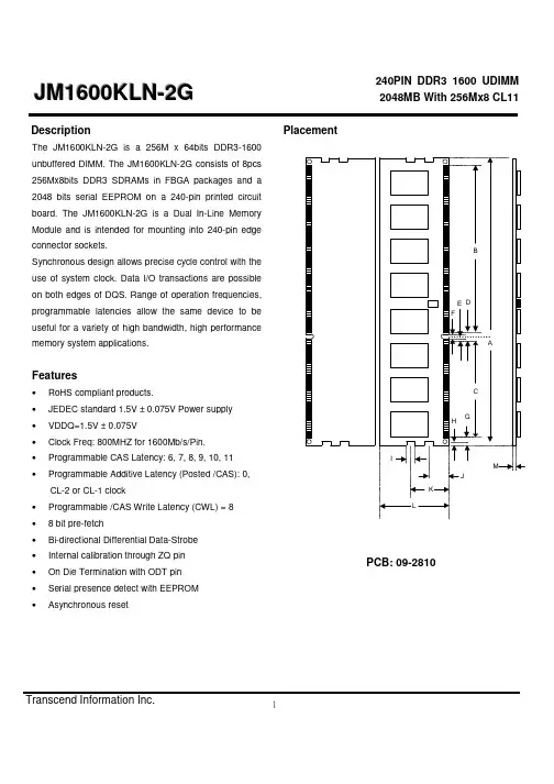
J M 1600K L N -2G2048MB With 256Mx8 CL11Transcend Information Inc.1DescriptionThe JM1600KLN-2G is a 256M x 64bits DDR3-1600 unbuffered DIMM. The JM1600KLN-2G consists of 8pcs 256Mx8bits DDR3 SDRAMs in FBGA packages and a 2048 bits serial EEPROM on a 240-pin printed circuit board. The JM1600KLN-2G is a Dual In-Line Memory Module and is intended for mounting into 240-pin edge connector sockets.Synchronous design allows precise cycle control with the use of system clock. Data I/O transactions are possible on both edges of DQS. Range of operation frequencies, programmable latencies allow the same device to be useful for a variety of high bandwidth, high performance memory system applications.Features• RoHS compliant products.• JEDEC standard 1.5V ± 0.075V Power supply • VDDQ=1.5V ± 0.075V• Clock Freq: 800MHZ for 1600Mb/s/Pin. • Programmable CAS Latency: 6, 7, 8, 9, 10, 11 • Programmable Additive Latency (Posted /CAS): 0, CL-2 or CL-1 clock• Programmable /CAS Write Latency (CWL) = 8 • 8 bit pre-fetch• Bi-directional Differential Data-Strobe • Internal calibration through ZQ pin • On Die Termination with ODT pin • Serial presence detect with EEPROM • Asynchronous resetPlacementPCB: 09-2810J M 1600K L N -2G2048MB With 256Mx8 CL11Transcend Information Inc.2DimensionsSide Millimeters Inches A 133.35±0.15 5.250±0.006 B 71 2.795 C 47 1.850 D 5 0.197 E 2.5 0.0980 F 1.5±0.10 0.059±0.039 G 5.175 0.204 H 2.311 0.091I 3±0.1 0.118±0.00394 J 9.5 0.374 K 17.3 0.681 L 30±0.15 1.181±0.006 M1.27±0.100.050±0.004(Refer Placement)Pin IdentificationSymbol FunctionA0~A15, BA0~BA2 Address Inputs/RAS Row Address Strobe /CAS Column Address Strobe /WE Write Enable /S0, /S1 Chip Selects CKE0, CKE1 Clock EnablesODT0, ODT1 On-die termination control DQ0~DQ63 Data Input/Output DQS0~DQS7 /DQS0~/DQS7 Data Strobe DM0~DM7 Data Masks CK0, /CK0 CK1, /CK1 Clocks Input /RESET Reset PinVDD Core and I/O Power VSS GroundVREFDQ VREFCA Input/Output Reference VTT Termination Voltage VDDSPD SPD Power SCL SPD Clock Input SDA SPD Data SA0~SA2 SPD Address NCNo ConnectionJ M 1600K L N -2G2048MB With 256Mx8 CL11Transcend Information Inc.3Pinouts:Pin No Pin Name Pin No Pin Name Pin No PinName Pin No Pin Name Pin No Pin Name Pin No Pin Name 01 VREFDQ 41 VSS 81 DQ32 121 VSS 161 NC 201 DQ37 02 VSS 42 NC 82 DQ33 122 DQ4 162 NC 202 VSS 03 DQ0 43 NC 83 VSS 123 DQ5 163 VSS 203 DM4 04 DQ1 44 VSS 84 /DQS4 124 VSS 164 NC 204 NC 05 VSS 45 NC 85 DQS4 125 DM0 165 NC 205 VSS 06 /DQS0 46 NC 86 VSS 126 NC 166 VSS 206 DQ38 07 DQS0 47 VSS 87 DQ34 127 VSS 167 NC 207 DQ39 08 VSS 48 NC 88 DQ35 128 DQ6 168 /RESET 208 VSS 09 DQ2 49 NC 89 VSS 129 DQ7 169 CKE1 209 DQ44 10 DQ3 50 CKE0 90 DQ40 130 VSS 170 VDD 210 DQ45 11 VSS 51 VDD 91 DQ41 131 DQ12 171 NC 211 VSS 12 DQ8 52 BA2 92 VSS 132 DQ13 172 NC 212 DM5 13 DQ9 53 NC 93 /DQS5 133 VSS 173 VDD 213 NC 14 VSS 54 VDD 94 DQS5 134 DM1 174 A12 214 VSS 15 /DQS1 55 A11 95 VSS 135 NC 175 A9 215 DQ46 16 DQS1 56 A7 96 DQ42 136 VSS 176 VDD 216 DQ47 17 VSS 57 VDD 97 DQ43 137 DQ14 177 A8 217 VSS 18 DQ10 58 A5 98 VSS 138 DQ15 178 A6 218 DQ52 19 DQ11 59 A4 99 DQ48 139 VSS 179 VDD 219 DQ53 20 VSS 60 VDD 100 DQ49 140 DQ20 180 A3 220 VSS 21 DQ16 61 A2 101 VSS 141 DQ21 181 A1 221 DM6 22 DQ17 62 VDD 102 /DQS6 142 VSS 182 VDD 222 NC 23 VSS 63 CK1 103 DQS6 143 DM2 183 VDD 223 VSS 24 /DQS2 64 /CK1 104 VSS 144 NC 184 CK0 224 DQ54 25 DQS2 65 VDD 105 DQ50 145 VSS 185 /CK0 225 DQ55 26 VSS 66 VDD 106 DQ51 146 DQ22 186 VDD 226 VSS 27 DQ18 67 VREFCA 107 VSS 147 DQ23 187 NC 227 DQ60 28 DQ19 68 NC 108 DQ56 148 VSS 188 A0 228 DQ61 29 VSS 69 VDD 109 DQ57 149 DQ28 189 VDD 229 VSS 30 DQ24 70 A10 110 VSS 150 DQ29 190 BA1 230 DM7 31 DQ25 71 BA0 111 /DQS7 151 VSS 191 VDD 231 NC 32 VSS 72 VDD 112 DQS7 152 DM3 192 /RAS 232 VSS 33 /DQS3 73 WE 113 VSS 153 NC 193 /S0 233 DQ62 34 DQS3 74 /CAS 114 DQ58 154 VSS 194 VDD 234 DQ63 35 VSS 75 VDD 115 DQ59 155 DQ30 195 ODT0 235 VSS 36 DQ26 76 /S1 116 VSS 156 DQ31 196 A13 236 VDDSPD 37 DQ27 77 ODT1 117 SA0 157 VSS 197 VDD 237 SA1 38 VSS 78 VDD 118 SCL 158 NC 198 NC 238 SDA 39 NC 79 NC 119 SA2 159 NC 199 VSS 239 VSS 40 NC 80 VSS 120 VTT160VSS200DQ36240 VTT。
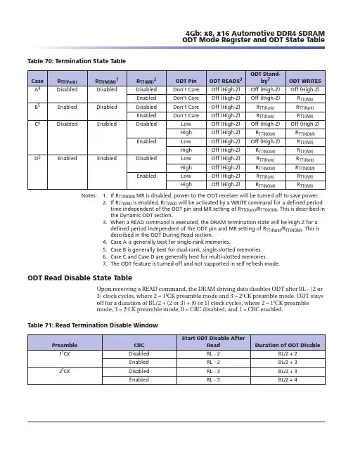
Table 70: Termination State TableNotes: 1.If R TT(NOM) MR is disabled, power to the ODT receiver will be turned off to save power.2.If R TT(WR) is enabled, R TT(WR) will be activated by a WRITE command for a defined period time independent of the ODT pin and MR setting of R TT(Park)/R TT(NOM). This is described in the Dynamic ODT section.3.When a READ command is executed, the DRAM termination state will be High-Z for a defined period independent of the ODT pin and MR setting of R TT(Park)/R TT(NOM). This isdescribed in the ODT During Read section.4.Case A is generally best for single-rank memories.5.Case B is generally best for dual-rank, single-slotted memories.6.Case C and Case D are generally best for multi-slotted memories.7.The ODT feature is turned off and not supported in self refresh mode.ODT Read Disable State TableUpon receiving a READ command, the DRAM driving data disables ODT after RL - (2 or3)clock cycles, where 2 = 1t CK preamble mode and 3 = 2t CK preamble mode. ODT stays off for a duration of BL/2 + (2 or 3) + (0 or 1) clock cycles, where 2 = 1t CK preamble mode, 3 = 2t CK preamble mode, 0 = CRC disabled, and 1 = CRC enabled.Table 71: Read Termination Disable Window4Gb: x8, x16 Automotive DDR4 SDRAM ODT Mode Register and ODT State TableElectrical SpecificationsAbsolute RatingsStresses greater than those listed may cause permanent damage to the device. This is a stress rating only, and functional operation of the device at these or any other condi-tions outside those indicated in the operational sections of this specification is not im-plied. Exposure to absolute maximum rating conditions for extended periods may ad-versely affect reliability. Although "unlimited" row accesses to the same row is allowed within the refresh period; excessive row accesses to the same row over a long term can result in degraded operation.Table 75: Absolute Maximum RatingsNotes: 1.V DD and V DDQ must be within 300mV of each other at all times, and V REF must not begreater than 0.6 × V DDQ . When V DD and V DDQ are <500mV, V REF can be ≤300mV.2.Storage temperature is the case surface temperature on the center/top side of theDRAM. For the measurement conditions, please refer to the JESD51-2 standard.3.V PP must be equal to or greater than V DD /V DDQ at all times when powered.DRAM Component Operating Temperature RangeOperating temperature, T OPER , is the case surface temperature on the center/top side of the DRAM. For measurement conditions, refer to the JEDEC document JESD51-2.Table 76: Temperature RangeNotes: 1.The normal temperature range specifies the temperatures at which all DRAM specifica-tions will be supported. During operation, the DRAM case temperature must be main-tained between –40°C to 85°C under all operating conditions for the commercial offer-ing.2.Some applications require operation of the commercial and industrial temperatureDRAMs in the extended temperature range (between 85°C and 125°C case tempera-ture). Full specifications are supported in this range, but the following additional condi-tions apply:•REFRESH commands must be doubled in frequency, reducing the refresh interval t REFI to 3.9μs. It is also possible to specify a component with 1X refresh (t REFI to 7.8μs) inthe extended temperature range.4Gb: x8, x16 Automotive DDR4 SDRAM Electrical Specificationsrate between the last crossing of V IH(DC)min and the first crossing of V IL(AC)max that does not ring back above V IL(DC)max .Hold (t IH) nominal slew rate for a rising signal is defined as the slew rate between the last crossing of V IL(DC)max and the first crossing of V IH(AC)min that does not ring back be-low V IH(DC)min . Hold (t IH) nominal slew rate for a falling signal is defined as the slew rate between the last crossing of V IH(DC)min and the first crossing of V IL(AC)min that does not ring back above V IL(DC)max .Table 87: Command and Address Setup and Hold Values Referenced – AC/DC-BasedTable 88: Derating Values for t IS/t IH – AC100DC75-Based4Gb: x8, x16 Automotive DDR4 SDRAM Electrical Characteristics – AC and DC Single-Ended Input Measurement Levels。
Micron M25P16 Serial Flash Embedded Memory16Mb, 3V Features•SPI bus compatible serial interface •16Mb Flash memory•75 MHz clock frequency (maximum)•2.7V to 3.6V single supply voltage•Page program (up to 256 bytes) in 0.64ms (TYP)•Erase capability–Sector erase: 512Kb in 0.6 s (TYP)–Bulk erase: 16Mb in 13 s (TYP)•Write protection–Hardware write protection: protected area size defined by non-volatile bits BP0, BP1, BP2•Deep power down: 1µA (TYP)•Electronic signature–JEDEC standard 2-byte signature (2015h)–Unique ID code (UID) and 16 bytes of read-only data, available upon customer request–RES command, one-byte signature (14h) for backward compatibility•More than 100,000 write cycles per sector •More than 20 years data retention •Automotive grade parts available •Packages (RoHS compliant)–SO8N (MN) 150 mils –SO8W (MW) 208 mils –SO16 (MF) 300 mils–VFDFPN8 (MP) MLP8 6mm x 5mm –VFDFPN8 (ME) MLP8 8mm x 6mm –UFDFPN8 (MC) MLP8 4mm x 3mmMicron M25P16 Serial Flash Embedded MemoryImportant Notes and WarningsFunctional DescriptionThe M25P16 is an 16Mb (2Mb x 8) serial Flash memory device with advanced write pro-tection mechanisms accessed by a high speed SPI-compatible bus. The device supports high-performance commands for clock frequency up to 75MHz.The memory can be programmed 1 to 256 bytes at a time using the PAGE PROGRAM command. It is organized as 32 sectors, each containing 256 pages. Each page is 256bytes wide. Memory can be viewed either as 8,192 pages or as 2,097,152 bytes. The en-tire memory can be erased using the BULK ERASE command, or it can be erased one sector at a time using the SECTOR ERASE command.This datasheet details the functionality of the M25P16 device based on 110nm process.Figure 1: Logic DiagramS#V CCHOLD#V SSDQ1C DQ0W#Table 1: Signal NamesMicron M25P16 Serial Flash Embedded MemoryFunctional DescriptionFigure 5: Bus Master and Memory Devices on the SPI BusSS2.Resistors (R) ensure that the memory device is not selected if the bus master leaves theS# line High-Z.3.The bus master may enter a state where all I/O are High-Z at the same time; for exam-ple, when the bus master is reset. Therefore, C must be connected to an external pull-down resistor so that when all I/O are High-Z, S# is pulled HIGH while C is pulled LOW.This ensures that S# and C do not go HIGH at the same time and that the t SHCH require-ment is met.4.The typical value of R is 100kΩ, assuming that the time constant R × C p (C p = parasiticcapacitance of the bus line) is shorter than the time during which the bus master leavesthe SPI bus High-Z.5.Example: Given that C p = 50pF (R × C p= 5μs), the application must ensure that the busmaster never leaves the SPI bus High-Z for a time period shorter than 5μs.质量等级领域:宇航级IC、特军级IC、超军级IC、普军级IC、禁运IC、工业级IC,军级二三极管,功率管等;应用领域:航空航天、船舶、汽车电子、军用计算机、铁路、医疗电子、通信网络、电力工业以及大型工业设备祝您:工作顺利,生活愉快!以深圳市美光存储技术有限公司提供的参数为例,以下为M25P16-VMC6TG的详细参数,仅供参考。
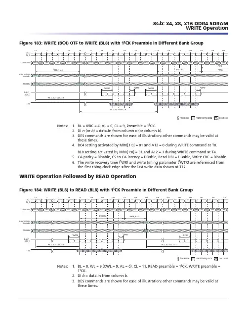
Figure 183: WRITE (BC4) OTF to WRITE (BL8) with 1t CK Preamble in Different Bank GroupCommand DQ CK_t CK_cDQS_t,DQS_cBank GroupAddress Address Notes: 1.BL = 8/BC = 4, AL = 0, CL = 9, Preamble = 1t CK.2.DI n (or b ) = data-in from column n (or column b ).3.DES commands are shown for ease of illustration; other commands may be valid atthese times.4.BC4 setting activated by MR0[1:0] = 01 and A12 = 0 during WRITE command at T0.BL8 setting activated by MR0[1:0] = 01 and A12 = 1 during WRITE command at T4.5.CA parity = Disable, CS to CA latency = Disable, Read DBI = Disable, Write CRC = Disable.6.The write recovery time (t WR) and write timing parameter (t WTR) are referenced fromthe first rising clock edge after the last write data shown at T17.WRITE Operation Followed by READ OperationFigure 184: WRITE (BL8) to READ (BL8) with 1t CK Preamble in Different Bank GroupCommand DQ CK_t CK_cDQS_t,DQS_cBank GroupAddress Address Notes: 1.BL = 8, WL = 9 (CWL = 9, AL = 0), CL = 11, READ preamble = 1t CK, WRITE preamble =1t CK.2.DI b = data-in from column b .3.DES commands are shown for ease of illustration; other commands may be valid atthese times.4.BL8 setting activated by either MR0[1:0] = 00 or MR0[1:0] = 01 and A12 = 1 duringWRITE command at T0 and READ command at T15.5.CA parity = Disable, CS to CA latency = Disable, Read DBI = Disable, Write DBI = Disable,Write CRC = Disable.6.The write timing parameter (t WTR_S) is referenced from the first rising clock edge afterthe last write data shown at T13.Figure 185: WRITE (BL8) to READ (BL8) with 1t CK Preamble in Same Bank GroupCommand DQ CK_t CK_c DQS_t,DQS_cBank GroupAddress Address Notes: 1.BL = 8, WL = 9 (CWL = 9, AL = 0), CL = 11, READ preamble = 1t CK, WRITE preamble =1t CK.2.DI b = data-in from column b .3.DES commands are shown for ease of illustration; other commands may be valid atthese times.4.BL8 setting activated by either MR0[1:0] = 00 or MR0[1:0] = 01 and A12 = 1 duringWRITE command at T0 and READ command at T17.5.CA parity = Disable, CS to CA latency = Disable, Read DBI = Disable, Write DBI = Disable,Write CRC = Disable.6.The write timing parameter (t WTR_L) is referenced from the first rising clock edge afterthe last write data shown at T13.Figure 186: WRITE (BC4) OTF to READ (BC4) OTF with 1t CK Preamble in Different Bank GroupCommand DQ CK_t CK_cDQS_t,DQS_cBank GroupAddress Address Notes: 1.BC = 4, WL = 9 (CWL = 9, AL = 0), CL = 11, READ preamble = 1t CK, WRITE preamble =1t CK.2.DI b = data-in from column b .3.DES commands are shown for ease of illustration; other commands may be valid atthese times.4.BC4 setting activated by MR0[1:0] = 01 and A12 = 0 during WRITE command at T0 andREAD command at T15.5.CA parity = Disable, CS to CA latency = Disable, Read DBI = Disable, Write DBI = Disable,Write CRC = Disable.6.The write timing parameter (t WTR_S) is referenced from the first rising clock edge afterthe last write data shown at T13.Figure 187: WRITE (BC4) OTF to READ (BC4) OTF with 1tCK Preamble in Same Bank GroupCommand DQ CK_t CK_cDQS_t,DQS_cBank GroupAddress Address Notes: 1.BC = 4, WL = 9 (CWL = 9, AL = 0), CL = 11, READ preamble = 1t CK, WRITE preamble =1t CK.2.DI b = data-in from column b .3.DES commands are shown for ease of illustration; other commands may be valid atthese times.4.BC4 setting activated by MR0[1:0] = 01 and A12 = 0 during WRITE command at T0 andREAD command at T17.8Gb: x4, x8, x16 DDR4 SDRAM WRITE Operation。
镁光ddr3内存颗粒编码规则全文共四篇示例,供读者参考第一篇示例:镁光DDR3内存颗粒编码规则是指在内存颗粒生产过程中所遵循的一系列规则和标准,以确保各个内存颗粒的质量与稳定性。
这些规则包括了内存颗粒的物理特性、电气性能、编码规范等方面,对于保证内存颗粒的正常运行和提高内存产品的稳定性具有重要意义。
镁光DDR3内存颗粒编码规则对内存颗粒的物理特性有着详细要求。
这包括内存颗粒的尺寸、结构、材料等方面。
内存颗粒的尺寸应该符合标准规定,确保能够与主板插槽匹配,并保证内存稳定性。
内存颗粒的结构应该牢固,避免碎裂或损坏。
内存颗粒的材料也应符合相关标准,确保内存颗粒的性能和稳定性。
镁光DDR3内存颗粒编码规则对内存颗粒的电气性能有着严格要求。
内存颗粒在工作中需要具有良好的电气性能,包括稳定的电压供应、低功耗、高频率等方面。
内存颗粒编码规则规定了内存颗粒的电气参数范围,确保内存颗粒在各种工作环境下都能够正常工作,不会因为电气问题导致数据丢失或系统崩溃。
镁光DDR3内存颗粒编码规则还对内存颗粒的编码规范有着详细的规定。
内存编码规范是指镁光DDR3内存颗粒的序列号、生产日期、批次信息等内容的编码规则。
通过严格遵守编码规范,可以方便内存产品的生产管理、质量控制和售后服务。
内存编码规范也能够帮助用户了解和识别内存产品的信息,确保产品的正常使用。
第二篇示例:镁光DDR3内存颗粒编码规则是指在制造镁光DDR3内存颗粒时所需遵循的一系列规定和标准。
内存颗粒是计算机存储器的关键组成部分,其性能和稳定性直接影响计算机系统的运行效果。
为了确保内存颗粒的质量和稳定性,制造商在生产过程中会严格遵循编码规则。
镁光DDR3内存颗粒编码规则规定了内存颗粒的各项参数和性能指标。
这些指标包括颗粒的规格、容量、速度等。
通过对这些参数的规定,可以确保生产出的内存颗粒符合标准,能够满足用户需求。
编码规则还规定了内存颗粒的生产工艺和质量控制要求。
在生产过程中,制造商需要严格按照规定的工艺流程进行操作,确保内存颗粒的制作过程受到控制,避免出现质量问题。
镁光和三星内存哪个好镁光和三星内存哪个好呢?小编来像你介绍!下面由小编给你做出详细的镁光和三星内存介绍!希望对你有帮助!镁光和三星内存介绍三三星(samsung)内存工艺整体上要领先其他内存颗粒制造厂。
三星的半导体晶片在存储行业内名声显赫,他们不仅有最先进的半导体技术,在存储晶片方面也走在世界的前端。
从全球的市场份额来看,三星也绝对称的上是大哥级别的!金士顿、威刚、海盗船等一线内存品牌都普遍使用三星的原厂颗粒以保证产品的性能。
三星金条依靠自家生产的内存颗粒一直保持着高品质内存的形象,价格比同规格其他品牌的产品也要略高。
镁光(micron)曾经被叫做美凯龙,是世界第二大内存颗粒制造商,但其产品在国内却不多见镁光和三星内存介绍三这两个品牌的内存条,一样好,随便选哪个都可以。
如有特殊需求,可考虑如下特点:1、三星和金士顿,都以稳定性好和兼容性好而著称。
都是好内存。
2、金士顿更偏重于兼容性。
所以,不惜损失性能去最大程度的提高兼容性。
因此,速度稍慢,但兼容性最好。
3、三星的内存,属于兼顾。
在保持比较好的兼容性的同时,稍微兼顾一下性能。
超频性能多数情况下要比金士顿好。
镁光和三星内存介绍三:2个厂商看谁的产品好,不光是从质量上来说的。
还看谁的售后好。
当然内存都是3年之内不会坏的,但是你们知道吗3年后这东西很容易报销。
5年以上的很少。
所以,我认为还是金士顿的好,虽然金士顿使用的是三星的颗粒,但是在高端市场上金士顿的研发组还是最强的。
最早看见金士顿的生产了16GB单条的内存条。
售价2000美元。
三星就不行。
但是,说实话,买内存,金士顿的假的比真的还多,也不能说是假的,只能说水货多。
很多。
所以这个问题,楼主问的让大家都不知所云。
看了“镁光和三星内存哪个好”文章的还看了:1.5000元台式电脑配置华硕主板cpuintel四核2.家用电脑配置大全推荐家用电脑DIY清单。
fresh mode, the DLL remains disabled even upon exit of SELF REFRESH operation untilit is re-enabled and reset.The DRAM is not tested to check—nor does Micron warrant compliance with—normalmode timings or functionality when the DLL is disabled. An attempt has been made tohave the DRAM operate in the normal mode where reasonably possible when the DLLhas been disabled; however, by industry standard, a few known exceptions are defined:•ODT is not allowed to be used•The output data is no longer edge-aligned to the clock•CL and CWL can only be six clocksWhen the DLL is disabled, timing and functionality can vary from the normal operationspecifications when the DLL is enabled (see DLL Disable Mode (page 125)). Disablingthe DLL also implies the need to change the clock frequency (see Input Clock Frequen-cy Change (page 129)).Output Drive StrengthThe DDR3 SDRAM uses a programmable impedance output buffer. The drive strengthmode register setting is defined by MR1[5, 1]. RZQ/7 (34ȍ [NOM]) is the primary outputdriver impedance setting for DDR3 SDRAM devices. To calibrate the output driver im-pedance, an external precision resistor (RZQ) is connected between the ZQ ball andV SSQ. The value of the resistor must be 240ȍ ±1%.The output impedance is set during initialization. Additional impedance calibration up-dates do not affect device operation, and all data sheet timings and current specifica-tions are met during an update.To meet the 34ȍ specification, the output drive strength must be set to 34ȍ during initi-alization. To obtain a calibrated output driver impedance after power-up, the DDR3SDRAM needs a calibration command that is part of the initialization and reset proce-dure.OUTPUT ENABLE/DISABLEThe OUTPUT ENABLE function is defined by MR1[12], as shown in Figure 56 (page146). When enabled (MR1[12] = 0), all outputs (DQ, DQS, DQS#) function when in thenormal mode of operation. When disabled (MR1[12] = 1), all DDR3 SDRAM outputs(DQ and DQS, DQS#) are tri-stated. The output disable feature is intended to be usedduring I DD characterization of the READ current and during t DQSS margining (writeleveling) only.TDQS EnableTermination data strobe (TDQS) is a feature of the x8 DDR3 SDRAM configuration thatprovides termination resistance (R TT) and may be useful in some system configurations.TDQS is not supported in x4 or x16 configurations. When enabled via the mode register(MR1[11]), the R TT that is applied to DQS and DQS# is also applied to TDQS and TDQS#.In contrast to the RDQS function of DDR2 SDRAM, DDR3’s TDQS provides the termina-tion resistance R TT only. The OUTPUT DATA STROBE function of RDQS is not providedby TDQS; thus, R ON does not apply to TDQS and TDQS#. The TDQS and DM functionsshare the same ball. When the TDQS function is enabled via the mode register, the DMfunction is not supported. When the TDQS function is disabled, the DM function is pro-vided, and the TDQS# ball is not used. The TDQS function is available in the x8 DDR32.RESET# is enabled LOW and used only for asynchronous reset. Thus, RESET# must beheld HIGH during any normal operation.3.The state of ODT does not affect the states described in this table.4.Operations apply to the bank defined by the bank address. For MRS, BA selects one offour mode registers.5.“V” means “H” or “L” (a defined logic level), and “X” means “Don’t Care.”6.See Table 71 (page 120) for additional information on CKE transition.7.Self refresh exit is asynchronous.8.Burst READs or WRITEs cannot be terminated or interrupted. MRS (fixed) and OTF BL/BCare defined in MR0.9.The purpose of the NOP command is to prevent the DRAM from registering any unwan-ted commands. A NOP will not terminate an operation that is executing.10.The DES and NOP commands perform similarly.11.The power-down mode does not perform any REFRESH operations.12.ZQ CALIBRATION LONG is used for either ZQinit (first ZQCL command during initializa-tion) or ZQoper (ZQCL command after initialization).。
Pin DescriptionsThe pin description table below is a comprehensive list of all possible pins for all DDR3modules. All pins listed may not be supported on this module. See Pin Assignments forinformation specific to this module.Table 6: Pin Descriptions质量等级领域:宇航级IC、特军级IC、超军级IC、普军级IC、禁运IC、工业级IC,军级二三极管,功率管等;应用领域:航空航天、船舶、汽车电子、军用计算机、铁路、医疗电子、通信网络、电力工业以及大型工业设备祝您:工作顺利,生活愉快!以深圳市美光存储技术有限公司提供的参数为例,以下为MT16KTF1G64HZ-1G6E1的详细参数,仅供参考Functional Block DiagramFigure 2: Functional Block Diagram (PCB 0900, R/C-F)S1#BA[2:0]A[15/14:0]RAS#CAS#WE#CKE0CKE1ODT0ODT1RESET#BA[2:0]: DDR3 SDRAMA[15/14:0]: DDR3 SDRAMRAS#: DDR3 SDRAMCAS#: DDR3 SDRAMCKE0: Rank 0CKE1: Rank 1ODT0: Rank 0VVVVVVCommand, address and clock line terminationsCK[1:0]CK#[1:0]Rank 0 = U1, U2, U7, U9, U11, U12, U17, U19Rank 1 = U5, U6, U8, U10, U15, U16, U18, U20DDNote: 1.The ZQ ball on each DDR3 component is connected to an external 240Ω ±1% resistor that is tied to ground. It is used for the calibration of the component’s ODT and outputdriver.Figure 3: Functional Block Diagram (PCB 1569, R/C-F3)S1#BA[2:0]A[14:0]RAS#CAS#WE#CKE0CKE1ODT0ODT1RESET#BA[2:0]: DDR3 SDRAMA[14:0]: DDR3 SDRAMRAS#: DDR3 SDRAMCAS#: DDR3 SDRAMWE#: DDR3 SDRAMCKE0: Rank 0CKE1: Rank 1ODT0: Rank 0ODT1: Rank 1RESET#: DDR3 SDRAMVVVV DDSPDVVCommand, address and clock line terminationsCK[1:0]CK#[1:0]Rank 0 = U2, U3, U6, U7, U8, U11, U12, U15Rank 1 = U4, U5, U7, U19, U13, U14, U16, U18DDNote: 1.The ZQ ball on each DDR3 component is connected to an external 240Ω ±1% resistor that is tied to ground. It is used for the calibration of the component’s ODT and outputdriver.。
Table 91: Derating Values for t IS/t IH – AC90/DC65-BasedData Receiver Input RequirementsThe following parameters apply to the data receiver Rx MASK operation detailed in theWrite Timing section, Data Strobe-to-Data Relationship.The rising edge slew rates are defined by srr1 and srr2. The slew rate measurementpoints for a rising edge are shown in the figure below. A LOW-to-HIGH transition time,tr1, is measured from 0.5 × V diVW,max below V CENTDQ,midpoint to the last transitionthrough 0.5 × V diVW,max above V CENTDQ,midpoint ; tr2 is measured from the last transitionthrough 0.5 × V diVW,max above V CENTDQ,midpoint to the first transition through the 0.5 ×V IHL(AC)min above V CENTDQ,midpoint .The falling edge slew rates are defined by srf1 and srf2. The slew rate measurementpoints for a falling edge are shown in the figure below. A HIGH-to-LOW transition time,tf1, is measured from 0.5 × V diVW,max above V CENTDQ,midpoint to the last transitionthrough 0.5 × V diVW,max below V CENTDQ,midpoint ; tf2 is measured from the last transitionthrough 0.5 × V diVW,max below V CENTDQ,midpoint to the first transition through the 0.5 ×V IHL(AC)min below V CENTDQ,midpoint .8Gb: x4, x8, x16 DDR4 SDRAM Electrical Characteristics – AC and DC Single-Ended Input Measurement Levels2.Micron recommends calibrating pull-up ODT resistors at 0.8 × V DDQ . Other calibrationschemes may be used to achieve the linearity specification shown here.3.The tolerance limits are specified under the condition that V DDQ = V DD and V SSQ = V SS .4.The DQ-to-DQ mismatch within byte variation for a given component including DQS_tand DQS_c.5.R TT variance range ratio to R TT nominal value in a given component, including DQS_tand DQS_c.DQ-to-DQ mismatch =R TT(MAX) - R TT(MIN)R TT(NOM)× 1006.DQ-to-DQ mismatch for a x16 device is treated as two separate bytes.7.For IT, AT, and UT devices, the minimum values are derated by 9% when the device op-erates between –40°C and 0°C (TC).ODT Temperature and Voltage SensitivityIf temperature and/or voltage change after calibration, the tolerance limits widen ac-cording to the following equations and tables.˂T = T - T(@ calibration); ˂V = V DDQ - V DDQ (@ calibration); V DD = V DDQTable 129: ODT Sensitivity DefinitionsTable 130: ODT Voltage and Temperature SensitivityODT Timing DefinitionsThe reference load for ODT timings is different than the reference load used for timingmeasurements.Figure 241: ODT Timing Reference Load8Gb: x4, x8, x16 DDR4 SDRAM Electrical Characteristics – On-Die Termination Characteristics。
DDR3 SDRAM RDIMMMT36JSF2G72PZ – 16GB Features•DDR3 functionality and operations supported as defined in the component data sheet•240-pin, registered dual in-line memory module (RDIMM)•Fast data transfer rates: PC3-14900, PC3-12800,PC3-10600, PC3-8500, or PC3-6400•16GB (2 Gig x 72)•V DD = 1.5V ±0.075V •V DDSPD = 3.0–3.6V•Supports ECC error detection and correction•Nominal and dynamic on-die termination (ODT) for data and strobe signals •Dual-rank•8 internal device banks•Fixed burst chop (BC) of 4 and burst length (BL) of 8via the mode register set (MRS)•On-board I 2C temperature sensor with integrated serial presence-detect (SPD) EEPROM •Gold edge contacts •Halogen-free •Fly-by topology•Terminated control, command, and address bus Figure 1: 240-Pin RDIMM (R/C J1)Figure 2: 240-Pin RDIMM (R/C E2)OptionsMarking•Operating temperature–Commercial (0°C ≤ T A ≤ 70°C)None •Package–240-pin DIMM (halogen-free)Z •Frequency/CAS latency– 1.07ns @ CL = 13 (DDR3-1866)-1G9– 1.25ns @ CL = 11 (DDR3-1600)-1G6– 1.5ns @ CL = 9 (DDR3-1333)-1G4– 1.87ns @ CL = 7 (DDR3-1066)-1G1Table 1: Key Timing ParametersTable 2: AddressingTable 3: Part Numbers and Timing Parameters – 16GB Modules1Notes: 1.The data sheet for the base device can be found on Micron’s web site.2.All part numbers end with a two-place code (not shown) that designates component and PCB revisions.Consult factory for current revision codes. Example: MT36JSF2G72PZ-1G4N1.Pin Assignments Table 4: Pin AssignmentsPin DescriptionsThe pin description table below is a comprehensive list of all possible pins for all DDR3modules. All pins listed may not be supported on this module. See Pin Assignments forinformation specific to this module.Table 5: Pin DescriptionsTable 5: Pin Descriptions (Continued)DQ MapsTable 6: Component-to-Module DQ Map (R/C J1), FrontTable 6: Component-to-Module DQ Map (R/C J1), Front (Continued)Table 7: Component-to-Module DQ Map (R/C J1), BackTable 7: Component-to-Module DQ Map (R/C J1), Back (Continued)Table 8: Component-to-Module DQ Map (R/C E2), FrontTable 9: Component-to-Module DQ Map (R/C E2), BackFunctional Block DiagramsFigure 3: Functional Block Diagram (R/C J1)V REFCAV SSV DD V DDSPDV TT V REFDQClock, control, command, and address line terminations:Rank 0: U1–U5, U8–U20 Rank 1: U21–U38RODT[1:0], TTDDNote:1.The ZQ ball on each DDR3 component is connected to an external 240Ω ±1% resistorthat is tied to ground. It is used for the calibration of the component’s ODT and output driver.Figure 4: Functional Block Diagram (R/C E2)V V V V V TT V Clock, control, command, and address line terminations:Rank 0: U1–U5, U12–U16, U21–U24, U31–U34 Rank 1: U8–U11, U17–U20, U26–U30, U35–U39RODT[1:0], R DDNote:1.The ZQ ball on each DDR3 component is connected to an external 240Ω ±1% resistorthat is tied to ground. It is used for the calibration of the component’s ODT and output driver.General DescriptionDDR3 SDRAM modules are high-speed, CMOS dynamic random access memory mod-ules that use internally configured 8-bank DDR3 SDRAM devices. DDR3 SDRAM mod-ules use DDR architecture to achieve high-speed operation. DDR3 architecture is essen-tially an 8n -prefetch architecture with an interface designed to transfer two data words per clock cycle at the I/O pins. A single read or write access for the DDR3 SDRAM mod-ule effectively consists of a single 8n -bit-wide, one-clock-cycle data transfer at the inter-nal DRAM core and eight corresponding n -bit-wide, one-half-clock-cycle data transfers at the I/O pins.DDR3 modules use two sets of differential signals: DQS, DQS# to capture data and CK and CK# to capture commands, addresses, and control signals. Differential clocks and data strobes ensure exceptional noise immunity for these signals and provide precise crossing points to capture input signals.Fly-By TopologyDDR3 modules use faster clock speeds than earlier DDR technologies, making signal quality more important than ever. For improved signal quality, the clock, control, com-mand, and address buses have been routed in a fly-by topology, where each clock, con-trol, command, and address pin on each DRAM is connected to a single trace and ter-minated (rather than a tree structure, where the termination is off the module near the connector). Inherent to fly-by topology, the timing skew between the clock and DQS sig-nals can be easily accounted for by using the write-leveling feature of DDR3.Registering Clock Driver OperationRegistered DDR3 SDRAM modules use a registering clock driver device consisting of a register and a phase-lock loop (PLL). The device complies with the JEDEC standard "Definition of the SSTE32882 Registering Clock Driver with Parity and Quad Chip Se-lects for DDR3 RDIMM Applications."The register section of the registering clock driver latches command and address input signals on the rising clock edge. The PLL section of the registering clock driver receives and redrives the differential clock signals (CK, CK#) to the DDR3 SDRAM devices. The register(s) and PLL reduce clock, control, command, and address signals loading by iso-lating DRAM from the system controller.Parity OperationsThe registering clock driver includes an even parity function for checking parity. The memory controller accepts a parity bit at the Par_In input and compares it with the data received on A[15:0], BA[2:0], RAS#, CAS#, and WE#. Valid parity is defined as an even number of ones (1s) across the address and command inputs (A[15:0], BA[2:0], RAS#,CAS#, and WE#) combined with Par_In. Parity errors are flagged on Err_Out#.Address and command parity is checked during all DRAM operations and during con-trol word WRITE operations to the registering clock driver. For SDRAM operations, the address is still propagated to the SDRAM even when there is a parity error. When writ-ing to the internal control words of the registering clock driver, the write will be ignored if parity is not valid. For this reason, systems must connect the Par_In pins on the DIMM and provide correct parity when writing to the registering clock driver control word configuration registers.16GB (x72, ECC, DR) 240-Pin DDR3 RDIMMGeneral DescriptionTemperature Sensor with Serial Presence-Detect EEPROMThermal Sensor OperationsThe temperature from the integrated thermal sensor is monitored and converts into a digital word via the I 2C bus. System designers can use the user-programmable registers to create a custom temperature-sensing solution based on system requirements. Pro-gramming and configuration details comply with JEDEC standard No. 21-C page 4.7-1,"Definition of the TSE2002av, Serial Presence Detect with Temperature Sensor."Serial Presence-Detect EEPROM OperationDDR3 SDRAM modules incorporate serial presence-detect. The SPD data is stored in a 256-byte EEPROM. The first 128 bytes are programmed by Micron to comply with JE-DEC standard JC-45, "Appendix X: Serial Presence Detect (SPD) for DDR3 SDRAM Mod-ules." These bytes identify module-specific timing parameters, configuration informa-tion, and physical attributes. The remaining 128 bytes of storage are available for use by the customer. System READ/WRITE operations between the master (system logic) and the slave EEPROM device occur via a standard I 2C bus using the DIMM’s SCL (clock)SDA (data), and SA (address) pins. Write protect (WP) is connected to V SS , permanently disabling hardware write protection. For further information refer to Micron technical note TN-04-42, "Memory Module Serial Presence-Detect."16GB (x72, ECC, DR) 240-Pin DDR3 RDIMMTemperature Sensor with Serial Presence-Detect EEPROMElectrical SpecificationsStresses greater than those listed may cause permanent damage to the module. This is a stress rating only, and functional operation of the module at these or any other condi-tions outside those indicated in each device's data sheet is not implied. Exposure to ab-solute maximum rating conditions for extended periods may adversely affect reliability.Table 10: Absolute Maximum RatingsTable 11: Operating ConditionsNotes:1.V TT termination voltage in excess of the stated limit will adversely affect the commandand address signals’ voltage margin and will reduce timing margins.2.T A and T C are simultaneous requirements.3.For further information, refer to technical note TN-00-08: “Thermal Applications,”available on Micron’s web site.4.The refresh rate is required to double when 85°C < T C ≤ 95°C.5.Inputs are terminated to V DD /2. Input current is dependent on terminating resistance se-lected in register.16GB (x72, ECC, DR) 240-Pin DDR3 RDIMMElectrical SpecificationsDRAM Operating ConditionsRecommended AC operating conditions are given in the DDR3 component data sheets.Component specifications are available on Micron’s web site. Module speed grades cor-relate with component speed grades, as shown below.Table 12: Module and Component Speed GradesDesign ConsiderationsSimulationsMicron memory modules are designed to optimize signal integrity through carefully de-signed terminations, controlled board impedances, routing topologies, trace lengthmatching, and decoupling. However, good signal integrity starts at the system level.Micron encourages designers to simulate the signal characteristics of the system'smemory bus to ensure adequate signal integrity of the entire memory system.PowerOperating voltages are specified at the DRAM, not at the edge connector of the module.Designers must account for any system voltage drops at anticipated power levels to en-sure the required supply voltage is maintained.I DD SpecificationsTable 13: DDR3 I DD Specifications and Conditions – 16GB (Die Revision D)Values are for the MT41J1G4 DDR3 SDRAM only and are computed from values specified in the 4GbNotes: 1.One module rank in the active I DD, the other rank in I DD2P0 (slow exit).2.All ranks in this I DD condition.Table 14: DDR3 I DD Specifications and Conditions – 16GB (Die Revisions E and J) Values are for the MT41J1G4 DDR3 SDRAM only and are computed from values specified in the 4GbNotes: 1.One module rank in the active I DD, the other rank in I DD2P0 (slow exit).2.All ranks in this I DD condition.Table 15: DDR3 I DD Specifications and Conditions – 16GB (Die Revision N)Values are for the MT41K1G4 DDR3 SDRAM only and are computed from values specified in the 4GbNotes: 1.One module rank in the active I DD, the other rank in I DD2P0 (slow exit).2.All ranks in this I DD condition.Registering Clock Driver SpecificationsTable 16: Registering Clock Driver Electrical CharacteristicsNote: 1.Timing and switching specifications for the register listed are critical for proper opera-tion of the DDR3 SDRAM RDIMMs. These are meant to be a subset of the parameters forthe specific device used on the module.Temperature Sensor with Serial Presence-Detect EEPROMThe temperature sensor continuously monitors the module's temperature and can beread back at any time over the I2C bus shared with the SPD EEPROM. Refer to JEDECstandard No. 21-C page 4.7-1, "Definition of the TSE2002av, Serial Presence Detect withTemperature Sensor."Serial Presence-DetectFor the latest SPD data, refer to Micron's SPD page: /SPD.Table 17: Temperature Sensor with SPD EEPROM Operating ConditionsTable 18: Temperature Sensor and SPD EEPROM Serial Interface TimingEVENT# PinThe temperature sensor also adds the EVENT# pin (open-drain). Not used by the SPDEEPROM, EVENT# is a temperature sensor output used to flag critical events that can beset up in the sensor’s configuration register.EVENT# has three defined modes of operation: interrupt mode, compare mode, andcritical temperature mode. Event thresholds are programmed in the 0x01 register usinga hysteresis. The alarm window provides a comparison window, with upper and lowerlimits set in the alarm upper boundary register and the alarm lower boundary register,respectively. When the alarm window is enabled, EVENT# will trigger whenever thetemperature is outside the MIN or MAX values set by the user.The interrupt mode enables software to reset EVENT# after a critical temperaturethreshold has been detected. Threshold points are set in the configuration register bythe user. This mode triggers the critical temperature limit and both the MIN and MAX ofthe temperature window.The compare mode is similar to the interrupt mode, except EVENT# cannot be reset bythe user and returns to the logic HIGH state only when the temperature falls below theprogrammed thresholds.Critical temperature mode triggers EVENT# only when the temperature has exceededthe programmed critical trip point. When the critical trip point has been reached, thetemperature sensor goes into comparator mode, and the critical EVENT# cannot becleared through software.Module DimensionsFigure 5: 240-Pin DDR3 RDIMM (R/C J1)Front view1.37 (0.054)1.17 (0.046)4.0 (0.157)0.50 (0.02) R(4X)15.0 (0.59)Notes:1.All dimensions are in millimeters (inches); MAX/MIN or typical (TYP) where noted.2.The dimensional diagram is for reference only.Figure 6: 240-Pin DDR3 RDIMM (R/C E2)Front view1.37 (0.054)1.17 (0.046)4.0 (0.157)15.0 (0.59)Notes: 1.All dimensions are in millimeters (inches); MAX/MIN or typical (TYP) where noted.2.The dimensional diagram is for reference only.8000 S. Federal Way, P.O. Box 6, Boise, ID 83707-0006, Tel: 208-368-3900/productsupport Customer Comment Line: 800-932-4992Micron and the Micron logo are trademarks of Micron Technology, Inc.All other trademarks are the property of their respective owners.This data sheet contains minimum and maximum limits specified over the power supply and temperature range set forth herein. Although considered final, these specifications are subject to change, as further product development and data characterization some-times occur.。