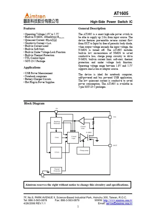
MAX16054AZTT中文资料
- 格式:pdf
- 大小:118.76 KB
- 文档页数:9
General DescriptionThe MAX16054 is a pushbutton on/off controller with a single switch debouncer and built-in latch. It accepts a noisy input from a mechanical switch and produces a clean latched digital output after a factory-fixed qualifi-cation delay.The MAX16054 eliminates contact bounce during switch opening and closing. The state of the output changes only when triggered by the falling edge of the debounced switch input; the output remains unchanged on the rising edge of the input. Robust switch inputs handle ±25V levels and are ±15kV ESD protected for use in harsh industrial environments. The MAX16054features a complementary output, OUT , which is the inverted state of OUT. An asynchronous CLEAR input allows an external signal to force the output flip-flop low.Undervoltage-lockout circuitry ensures that OUT is in the off state upon power-up. The MAX16054 requires no external components, and its low supply current makes it ideal for use in portable equipment.The MAX16054 operates from a +2.7V to +5.5V single supply. The MAX16054 is offered in a 6-pin thin SOT23package and operates over the -40°C to +125°C auto-motive temperature range.ApplicationsPDAsMP3/Video Players Portable Electronics Set-Top BoxesPortable Instrumentation White GoodsFeatureso Robust Inputs Can Handle Power Supplies Up to ±25V o ±15kV ESD Protection o Latched Outputo Low 7µA Supply Current o Operates from 2.7V to 5.5Vo -40°C to +125°C Temperature Range o Thin SOT23 PackageMAX16054On/Off Controller with Debounce and±15kV ESD Protection________________________________________________________________Maxim Integrated Products 1Pin ConfigurationOrdering InformationTypical Operating Circuits19-4128; Rev 0; 5/08For pricing, delivery, and ordering information,please contact Maxim Direct at 1-888-629-4642,or visit Maxim’s website at .+Denotes a lead-free package.T = Tape and reel package. Devices are offered in 2.5k unit increments.M A X 16054On/Off Controller with Debounce and ±15kV ESD Protection 2_______________________________________________________________________________________ABSOLUTE MAXIMUM RATINGSELECTRICAL CHARACTERISTICSStresses beyond those listed under “Absolute Maximum Ratings” may cause permanent damage to the device. These are stress ratings only, and functional operation of the device at these or any other conditions beyond those indicated in the operational sections of the specifications is not implied. Exposure to absolute maximum rating conditions for extended periods may affect device reliability.Note 1:As per JEDEC 51 standard, multilayer board (PCB).CC UVLO V CC to GND..............................................................-0.3V to +6V IN to GND................................................................-30V to +30V CLEAR to GND.........................................................-0.3V to +6V OUT, OUT to GND......................................-0.3V to (V CC + 0.3V)Short-Circuit DurationOUT, OUT to GND ...................................................Continuous Continuous Power Dissipation (T A = +70°C)6-Pin Thin SOT23(derate 9.1mW/°C at +70°C) (Note 1)............................727mW Operating Temperature Range .........................-40°C to +125°C Maximum Junction Temperature.....................................+150°C Storage Temperature Range.............................-60°C to +150°C Lead Temperature (soldering, 10s).................................+300°CMAX16054On/Off Controller with Debounce and±15kV ESD Protection_______________________________________________________________________________________3SUPPLY CURRENT vs. TEMPERATURETEMPERATURE (°C)S U P P L Y C U R R E N T (μA )110956580-105203550-25123456789100-40125DEBOUNCE OF CLOSING SWITCH10ms/div10VIN 10V/div -10V OUT 5V/div 0V OUT 5V/div 0VOUTPUT LOGIC LEVEL vs. SUPPLY VOLTAGESUPPLY VOLTAGE (V)O U T P U T L O G I C L E V E L (V )5.04.54.03.53.02.512345602.05.5Typical Operating Characteristics(T A = +25°C, unless otherwise noted.)DEBOUNCE DELAY PERIOD vs. TEMPERATURETEMPERATURE (°C)D E B O U N C E D E L A Y P E R I O D (m s )110956580-105203550-254244464850525456586040-40125V CC UNDERVOLTAGE LOCKOUTvs. TEMPERATURETEMPERATURE (°C)V C C U N D E R V O L T A G E L O C K O U T (V )1109580655035205-10-250.51.01.52.02.53.03.50-40125Detailed DescriptionTheory of OperationThe MAX16054 creates a push-on, push-off function using a momentary-contact normally open SPST switch. The high-to-low transition that occurs when closing the switch causes OUT to go high and OUT to go low. The output state remains latched after the switch is released/opened. Closing the switch again causes OUT to go low and OUT to go high.Debounce circuitry eliminates the extraneous level changes that result from interfacing with mechanical switches (switch bounce). Virtually all mechanical switches bounce upon opening and closing. The bounce when a switch opens or closes is eliminated by requiring that the sequentially clocked input remains in the same state for a number of sampling periods. Theoutput does not change state from high-to-low or low-to-high until the input is stable for at least 50ms (typ).The Functional Diagram shows the functional blocks consisting of an on-chip oscillator, counter, exclusive-NOR gate, a D flip-flop, and a T (toggle) flip-flop. When the pushbutton input does not equal the internal debounced button state (the Q output of the D flip-flop), the XNOR gate issues a counter reset. When the switch input state is stable for the full qualification peri-od, the counter clocks the D flip-flop, changing the internal pushbutton state. The Q output of the D flip-flop is connected to a toggle flip-flop that toggles when the internal pushbutton state goes through a high-to-low transition. Figure 1 shows the typical opening and clos-ing switch debounce operation.A rising pulse at CLEAR resets the T flip-flop and pulls OUT low and OUT high.M A X 16054On/Off Controller with Debounce and ±15kV ESD Protection 4_______________________________________________________________________________________Functional DiagramUndervoltage LockoutThe undervoltage-lockout circuitry ensures that the out-puts are at the correct state on power-up. While V CC is less than the 2.1V (typ) undervoltage threshold and greater than 1.0V, OUT remains low and transitions at IN are ignored.Robust Switch InputThe switch input (IN) has overvoltage clamping diodes to protect against damaging fault conditions. Switch input voltages can safely swing ±25V to ground. Proprietary ESD-protection structures protect against high ESD encountered in harsh industrial environments, membrane keypads, and portable applications. They are designed to withstand ±15kV per the IEC 61000-4-2 Air-Gap Discharge test and ±8kV per the IEC 61000-4-2 Contact-Discharge test.Since there is a 63k Ω(typ) pullup resistor connected to IN, driving the input to -25V draws approximately 0.5mA from the V CC supply. Driving the input to +25V causes approximately 0.32mA of current to flow back into the V CC supply. If the total system V CC supply current is less than the current flowing back into the V CC supply,V CC rises above normal levels. In some low-current sys-tems, a zener diode on V CC may be required.±15kV ESD ProtectionESD-protection structures are incorporated on all pins to protect against electrostatic discharges encountered during handling and assembly. The MAX16054 has extra protection against static electricity to protect against ESD of ±15kV at the switch input without dam-age. The ESD structures withstand high ESD in all states: normal operation, shutdown, and powered down. A design advantage of the MAX16054 is that it continues working without latchup after an ESD event,which eliminates the need to power-cycle the device.ESD protection can be tested in various ways; this product is characterized for protection to the following limits:1)±15kV using the Human Body Model.2)±8kV using the Contact-Discharge method specified in IEC 61000-4-2.3)±15kV using the IEC 61000-4-2 Air-Gap method.MAX16054On/Off Controller with Debounce and±15kV ESD Protection_______________________________________________________________________________________5Figure 1. MAX16054 Timing DiagramM A X 16054Human Body ModelFigure 2a shows the Human Body Model, and Figure 2b shows the current waveform it generates when dis-charged into a low impedance. This model consists of a 100pF capacitor charged to the ESD voltage of interest,which is then discharged into the test device through a 1.5k Ωresistor.IEC 61000-4-2The IEC 61000-4-2 standard covers ESD testing and performance of finished equipment; it does not specifi-cally refer to integrated circuits. The MAX16054 helps in the design of equipment that meets IEC 61000-4-2, with-out the need for additional ESD-protection components.The major difference between tests done using the Human Body Model and IEC 61000-4-2 is higher peak current in IEC 61000-4-2, because series resistance islower in the IEC 61000-4-2 model. Hence, the ESD with-stand voltage measured to IEC 61000-4-2 is generally lower than that measured using the Human Body Model.Figure 3a shows the IEC 61000-4-2 model, and Figure 3b shows the current waveform for the IEC 61000-4-2ESD Contact-Discharge test.The Air-Gap test involves approaching the device with a charged probe. The Contact-Discharge method connects the probe to the device before the probe is energized.Machine ModelThe Machine Model for ESD tests all pins using a 200pF storage capacitor and zero discharge resis-tance. Its objective is to emulate the stress caused by contact that occurs with handling and assembly during manufacturing.On/Off Controller with Debounce and ±15kV ESD Protection 6_______________________________________________________________________________________Figure 2a. Human Body ESD Test ModelFigure 2b. Human Body Current WaveformFigure 3a. IEC 61000-4-2 ESD Test ModelFigure 3b. IEC 61000-4-2 ESD Generator Current WaveformMAX16054On/Off Controller with Debounce and±15kV ESD Protection_______________________________________________________________________________________7Typical Operating Circuits (continued)M A X 16054On/Off Controller with Debounce and ±15kV ESD Protection 8_______________________________________________________________________________________Typical Operating Circuits (continued)MAX16054On/Off Controller with Debounce and±15kV ESD ProtectionMaxim cannot assume responsibility for use of any circuitry other than circuitry entirely embodied in a Maxim product. No circuit patent licenses are implied. Maxim reserves the right to change the circuitry and specifications without notice at any time.Maxim Integrated Products, 120 San Gabriel Drive, Sunnyvale, CA 94086 408-737-7600 _____________________9©2008 Maxim Integrated Productsis a registered trademark of Maxim Integrated Products, Inc.Package InformationFor the latest package outline information, go to /packages .Chip InformationPROCESS: BiCMOS。