半导体物理习题课-第八章
- 格式:ppt
- 大小:279.50 KB
- 文档页数:13
半导体物理习题 -CAL-FENGHAI-(2020YEAR-YICAI)_JINGBIAN附: 半导体物理习题第一章 晶体结构1. 指出下述各种结构是不是布拉伐格子。
如果是,请给出三个原基矢量;如果不是,请找出相应的布拉伐格子和尽可能小的基元。
(1) 底心立方(在立方单胞水平表面的中心有附加点的简立方); (2) 侧面心立方(在立方单胞垂直表面的中心有附加点的简立方); (3) 边心立方(在最近邻连线的中点有附加点的简立方)。
2. 证明体心立方格子和面心立方格子互为正、倒格子。
3. 在如图1所示的二维布拉伐格子中,以格点O 为原点,任意选取两组原基矢量,写出格点A 和B 的晶格矢量A R 和B R 。
4. 以基矢量为坐标轴(以晶格常数a 为度量单位,如图2),在闪锌矿结构的一个立方单胞中,写出各原子的坐标。
5.石墨有许多原子层,每层是由类似于蜂巢的六角形原子环组成,使每个原子有距离为a的三个近邻原子。
试证明在最小的晶胞中有两个原子,并画出正格子和倒格子。
第二章晶格振动和晶格缺陷1.质量为m和M的两种原子组成如图3所示的一维复式格子。
假设相邻原子间的弹性力常数都是β,试求出振动频谱。
2.设有一个一维原子链,原子质量均为m,其平衡位置如图4所示。
如果只考虑相邻原子间的相互作用,试在简谐近似下,求出振动频率ω与波矢q之间的函数关系。
3.若把聚乙烯链—CH=CH—CH=CH—看作是具有全同质量m、但力常数是以1β,2β交替变换的一维链,链的重复距离为a,试证明该一维链振动的特征频率为}])(2sin41[1{2/1221221212ββββββω+-±+=qam并画出色散曲线。
第三章 半导体中的电子状态1. 设晶格常数为a 的一维晶格,导带极小值附近的能量)(k E c 为mk k m k k E c 21222)(3)(-+=(3.1)价带极大值附近的能量)(k E v 为mk m k k E v 2221236)( -=(3.2)式中m 为电子质量,14.3,/1==a a k πÅ。

半导体物理习题第八章答案半导体物理习题第八章答案第一题:根据题目要求,我们需要计算一个p型半导体的载流子浓度。
根据半导体物理的知识,p型半导体中主要存在的是空穴载流子,因此我们需要计算空穴浓度。
在p型半导体中,空穴浓度可以通过以下公式计算:p = ni^2 / n其中,p表示空穴浓度,ni表示本征载流子浓度,n表示杂质浓度。
根据题目给出的数据,本征载流子浓度ni为2.5 x 10^16 cm^-3,杂质浓度n为1 x10^16 cm^-3。
将这些数据代入公式中,我们可以得到:p = (2.5 x 10^16 cm^-3)^2 / (1 x 10^16 cm^-3) = 6.25 x 10^16 cm^-3因此,该p型半导体的空穴浓度为6.25 x 10^16 cm^-3。
第二题:第二题要求我们计算一个n型半导体的载流子浓度。
根据半导体物理的知识,n 型半导体中主要存在的是电子载流子,因此我们需要计算电子浓度。
在n型半导体中,电子浓度可以通过以下公式计算:n = ni^2 / p其中,n表示电子浓度,ni表示本征载流子浓度,p表示空穴浓度。
根据题目给出的数据,本征载流子浓度ni为2.5 x 10^16 cm^-3,空穴浓度p为5 x10^15 cm^-3。
将这些数据代入公式中,我们可以得到:n = (2.5 x 10^16 cm^-3)^2 / (5 x 10^15 cm^-3) = 12.5 x 10^16 cm^-3因此,该n型半导体的电子浓度为12.5 x 10^16 cm^-3。
第三题:第三题要求我们计算一个p-n结的内建电势。
根据半导体物理的知识,p-n结的内建电势可以通过以下公式计算:Vbi = (kT / q) * ln(Na * Nd / ni^2)其中,Vbi表示内建电势,k表示玻尔兹曼常数,T表示温度,q表示电子电荷量,Na和Nd分别表示p型和n型半导体中杂质浓度,ni表示本征载流子浓度。

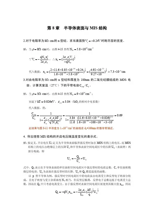
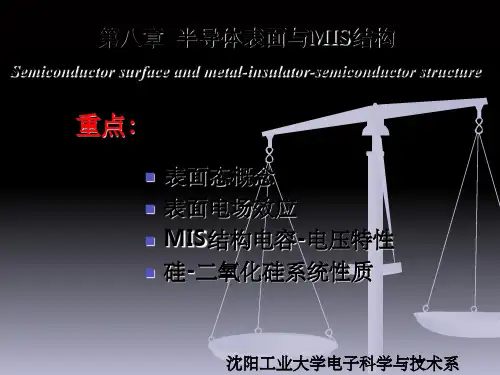
第8章 半导体表面与MIS 结构2.对于电阻率为8cm Ω⋅的n 型硅,求当表面势0.24s V V =-时耗尽层的宽度。
解:当8cm ρ=Ω⋅时:由图4-15查得1435.810D N cm -=⨯∵22D d s rs qN x V εε=-,∴1022()rs s d D V x qN εε=-代入数据:11141352219145211.68.85100.24 4.9210()()7.3101.610 5.8109.2710d x cm -----⨯⨯⨯⨯⨯==⨯⨯⨯⨯⨯3.对由电阻率为5cm Ω⋅的n 型硅和厚度为100nm 的二氧化硅膜组成的MOS 电容,计算其室温(27℃)下的平带电容0/FB C C 。
解:当5cm ρ=Ω⋅时,由图4-15查得143910D N cm -=⨯;室温下0.026eV kT =,0 3.84r ε=(SiO 2的相对介电系数) 代入数据,得:1141/20002197722110.693.84(11.68.85100.026)11()11.6 1.61010010310FBr rs rs A C C kT q N d εεεε---===⨯⨯⨯+⋅+⨯⨯⨯⨯⨯此结果与图8-11中浓度为1⨯1015/cm 3的曲线在d 0=100nm 的值非常接近。
4. 导出理想MIS 结构的开启电压随温度变化的表示式。
解:按定义,开启电压U T 定义为半导体表面临界强反型时加在MOS 结构上的电压,而MOS结构上的电压由绝缘层上的压降U o 和半导体表面空间电荷区中的压降U S (表面势)两部分构成,即oST S Q U U C =-+ 式中,Q S 表示在半导体表面的单位面积空间电荷区中强反型时的电荷总数,C o 单位面积绝缘层的电容,U S 为表面在强反型时的压降。
U S 和Q S 都是温度的函数。
以p 型半导体为例,强反型时空间电荷区中的电荷虽由电离受主和反型电子两部分组成,且电子密度与受主杂质浓度N A 相当,但反型层极薄,反型电子总数远低于电离受主总数,因而在Q S 中只考虑电离受主。
半导体物理与器件习题目录半导体物理与器件习题 (1)一、第一章固体晶格结构 (2)二、第二章量子力学初步 (2)三、第三章固体量子理论初步 (2)四、第四章平衡半导体 (3)五、第五章载流子输运现象 (5)六、第六章半导体中的非平衡过剩载流子 (5)七、第七章pn结 (6)八、第八章pn结二极管 (6)九、第九章金属半导体和半导体异质结 (7)十、第十章双极晶体管 (7)十一、第十一章金属-氧化物-半导体场效应晶体管基础 (8)十二、第十二章MOSFET概念的深入 (9)十三、第十三章结型场效应晶体管 (9)一、第一章固体晶格结构1.如图是金刚石结构晶胞,若a 是其晶格常数,则其原子密度是。
2.所有晶体都有的一类缺陷是:原子的热振动,另外晶体中常的缺陷有点缺陷、线缺陷。
3.半导体的电阻率为10-3~109Ωcm。
4.什么是晶体?晶体主要分几类?5.什么是掺杂?常用的掺杂方法有哪些?答:为了改变导电性而向半导体材料中加入杂质的技术称为掺杂。
常用的掺杂方法有扩散和离子注入。
6.什么是替位杂质?什么是填隙杂质?7.什么是晶格?什么是原胞、晶胞?二、第二章量子力学初步1.量子力学的三个基本原理是三个基本原理能量量子化原理、波粒二相性原理、不确定原理。
2.什么是概率密度函数?3.描述原子中的电子的四个量子数是:、、、。
三、第三章固体量子理论初步1.能带的基本概念◼能带(energy band)包括允带和禁带。
◼允带(allowed band):允许电子能量存在的能量范围。
◼禁带(forbidden band):不允许电子存在的能量范围。
◼允带又分为空带、满带、导带、价带。
◼空带(empty band):不被电子占据的允带。
◼满带(filled band):允带中的能量状态(能级)均被电子占据。
导带:有电子能够参与导电的能带,但半导体材料价电子形成的高能级能带通常称为导带。
价带:由价电子形成的能带,但半导体材料价电子形成的低能级能带通常称为价带。


Chapter 88.1In forward bias Then or (a)For 1021=f f I I , thenor6.5921=-V V mV 60≅mV (b)For 10021=f f I I , thenor3.11921=-V V mV 120≅mV_______________________________________ 8.2()4152102108125.2108105.1⨯=⨯⨯==a i po N n n cm 3-()515210210125.1102105.1⨯=⨯⨯==d i no N n p cm 3-(a) 45.0=a V V,121095.3⨯=cm 3- or()111088.9⨯=-p p x n cm 3- (b) 55.0=a V V,141088.1⨯=cm 3- 131069.4⨯=cm 3- (c) 55.0-=a V V_______________________________________ 8.3()516262101.8104108.1-⨯=⨯⨯==a i po N n n cm 3-()4162621024.310108.1-⨯=⨯==d i noN n p cm 3-(a) 90.0=a V V,11100.4⨯=cm 3- 10100.10⨯=cm 3- (b) 10.1=a V V141003.9⨯=cm 3-141026.2⨯=cm 3-_______________________________________ 8.43105.4⨯=cm 3-4105.4⨯=cm 3-(i)()⎪⎪⎭⎫⎝⎛=t a no n n V V p x p exp or ()⎥⎦⎤⎢⎣⎡=no n n t a p x p V V ln599.0=V (ii) n-region - lower doped side 410214.3⨯=cm 3-3105.7⨯=cm 3-(i) ()⎥⎥⎦⎤⎢⎢⎣⎡=po a t a n N V V 1.0ln6165.0=V(ii) p-region - lower doped side_______________________________________ 8.5849.1=A/cm 2()()()849.1103-=-=p n n x AJ I Aor 85.1=n I mA521.4=A/cm 2()()()521.4103-==n p p x AJ I Aor 52.4=p I mA(a) 37.652.485.1=+=+=p n I I I mA _______________________________________ 8.6For an p n + silicon diode or15108.1-⨯=S I A (a) For 5.0=a V V, or71036.4-⨯=D I A(b) For 5.0-=a V V, or15108.1-⨯-=-≅S D I I A_______________________________________ 8.7410568.1-⨯=s J A/cm 2 41044.2-⨯= A or 244.0=I mA810568.1-⨯-= A_______________________________________ 8.81110145.5-⨯=s J A/cm 2 1410029.1-⨯= A (i)()⎪⎭⎫ ⎝⎛⨯=-0259.045.0exp 10029.114I71061.3-⨯= A(ii)()⎪⎭⎫⎝⎛⨯=-0259.055.0exp 10029.114I51072.1-⨯= A (iii)()⎪⎭⎫ ⎝⎛⨯=-0259.065.0exp 10029.114I 41016.8-⨯= A_______________________________________ 8.9We haveor we can write this as so thatIn reverse bias, I is negative, so at90.0-=SI I, we haveor6.59-=V mV_______________________________________ 8.10Case 1: ⎪⎪⎭⎫⎝⎛=t a s V V I I exp1510305.6-⨯=⇒s I A 1210305.6-⨯=mA 810153.3-⨯=mA/cm 2Case 2: ⎪⎪⎭⎫⎝⎛=t a s V V I I exp or 093.1=I mA9102-⨯=mA/cm 2Case 3: ⎪⎪⎭⎫⎝⎛=t a s V V AJ I exp So ⎥⎦⎤⎢⎣⎡=s t a AJ I V V ln6502.0=a V V Then()()1174101010---===s s AJ I mACase 4: ⎪⎭⎫ ⎝⎛=⎪⎪⎭⎫ ⎝⎛=0259.072.0exp 20.1exp ta s V V I I1210014.1-⨯=s I mA 51007.5-⨯=cm 2 _______________________________________ 8.1107857.0=da N Nor73.12=adN N (a) From part (a),828.2=daN N or 354.0=adN N _______________________________________ 8.12The cross-sectional area is43105201010--⨯=⨯==J I A cm 2We have which yields1010522.2-⨯=S J A/cm 2 We can write We want or=()10.010472.410071.710071.7333=⨯+⨯⨯da N Nwhich yields Now We find141009.7⨯=d N cm 3- and161001.1⨯=a N cm 3-_______________________________________ 8.13Plot_______________________________________ 8.14 (a)We have4.21==np np D D μμ and 1.01=po no ττ soor(b) Using Einstein's relation, we can write We haved n n Ne μσ= and a p p N e μσ= Also Then_______________________________________ 8.15(a) p-side; or329.0=-F Fi E E eV Also on the n-side; or407.0=-Fi F E E eV (b) We can find()()4.320259.01250==n D cm 2/s ()()29.80259.0320==p D cm 2/sNow or1110426.4-⨯=S J A/cm 2 Then or1510426.4-⨯=S I A We find or61007.1-⨯=I A μ07.1= A (c) The hole current is or⎪⎪⎭⎫⎝⎛⨯=-t D p V V I exp 10278.316 (A) Then_______________________________________ 8.161410342.1-⨯=sp I A ()()()162107419105105.110225105106.1⨯⨯⋅⨯⨯⨯=--- 1510025.4-⨯=sn I A746826.0=V()()()59746.0746826.08.08.0===bi a V V V 141056.1⨯=cm 3- 5101981.4-⨯= A 4103997.1-⨯= A 410820.1-⨯= ANow5104896.8-⨯= A Then510710.9-⨯= A_______________________________________ 8.17(a) The excess hole concentration is given byWe find()41621021025.210105.1⨯=⨯==d i no N n p cm 3- and410828.2-⨯=cm μ828.2=m Then or()⎪⎭⎫⎝⎛⨯-⨯=-41410828.2exp 1081.3x p n δ cm 3-(b) We haveAt 4103-⨯=x cm, or()5966.03=p J A/cm 2 (c) We haveWe can determine that3105.4⨯=po n cm 3- andμ72.10=n L m Then or2615.0=no J A/cm 2 We can also find724.1=po J A/cm 2Then at μ3=x m, or()39.13=n J A/cm 2_______________________________________ 8.18 (a) Problem 8.7 or()⎥⎥⎦⎤⎢⎢⎣⎡=⎪⎪⎭⎫ ⎝⎛=a i a t po p t a N n N V n n V V 21.0ln ln 205.0=V (b) Problem 8.8or ⎥⎦⎤⎢⎣⎡=no n t a p p V V ln ()⎥⎥⎦⎤⎢⎢⎣⎡=d i d t N n N V 21.0ln623.0=V_______________________________________8.19The excess electron concentration is given byThe total number of excess electrons is We may note that ThenWe find that25=n D cm 2/s and μ0.50=n L m Also()41521021081.2108105.1⨯=⨯⨯==a i po N n n cm 3- Then orThen, we find the total number of excess electrons in the p-region to be: (a)3.0=a V V, 41051.1⨯=p N(b)4.0=a V V, 51017.7⨯=p N (c)5.0=a V V, 71040.3⨯=p N Similarly, the total number of excess holes inthe n-region is found to be We find that0.10=p D cm 2/s and μ0.10=p L mAlso()41621021025.210105.1⨯=⨯==d i no N n p cm 3- Then So(a)3.0=a V V, 31041.2⨯=n P(b)4.0=a V V, 51015.1⨯=n P (c)5.0=a V V, 61045.5⨯=n P_______________________________________ 8.20Then so orWe then have or Then or769.02=g E eV_______________________________________ 8.21(a) We havewhich can be written in the form or(b) Taking the ratioFor 3001=T K, 0259.01=kT ,61.3811=kT For 4002=T K, 03453.02=kT , 96.2812=kT (i) Germanium: 66.0=g E eV or138312=S S I I (ii) Silicon: 12.1=g E eVor5121017.1⨯=S S I I _______________________________________ 8.22Plot_______________________________________ 8.23First case: or()05049.0102ln 50.0ln 4=⨯==sf a t I I V V VNow ()⎪⎭⎫⎝⎛=3000259.005049.0T8.584=⇒T K Second case:or 272102519.8⨯=i n NowBy trial and error, 502≅T KThe reverse-bias current is limiting factor. _______________________________________ 8.24()()37101010--===po p p D L τcmor μ10=p L m; p n L W <<⇒(i)()()⎪⎪⎭⎫ ⎝⎛==tano d n n VV p N x p exp 1.0 or ()⎥⎥⎦⎤⎢⎢⎣⎡=221.0ln i d t a n N V V 5516.0=a V V(ii)⎪⎪⎭⎫⎝⎛⎪⎪⎭⎫ ⎝⎛=t ad i n p p V VN n W AeD I exp 2310565.4-⨯=p I A 61026.2-⨯=n I A 310567.4-⨯= A or 567.4=I mA (b)(i)()()⎪⎪⎭⎫⎝⎛==-t a po a p p V V n N x n exp 1.0 or ()⎥⎥⎦⎤⎢⎢⎣⎡=221.0ln i a t a n N V V 5516.0=a V V (ii)⎪⎪⎭⎫⎝⎛⎪⎪⎭⎫ ⎝⎛=t adi n p p V VN n W AeD I exp 2 510565.4-⨯=p I A 4102597.2-⨯=n I A 410716.2-⨯= A or 2716.0=I mA_______________________________________ 8.25(a) We can write for the n-region The general solution is of the formThe boundary condition at n x x =gives and the boundary condition at n n W x x += givesFrom this equation, we haveThen, from the first boundary condition, weobtainWe then obtainwhich can be written as We can also findThe solution can now be written as or finally (b)=⎪⎪⎭⎫⎝⎛⎥⎥⎦⎤⎢⎢⎣⎡-⎪⎪⎭⎫ ⎝⎛-p n t a no p L W V V p eD sinh 1expThen_______________________________________ 8.26For the temperature range 320300≤≤T K,neglect the change in c N and υN . ThenTaking the ratio of currents, but maintainingD I a constant, we have We then have We have300=T K , 60.01=D V V and 0259.01=kT eV,0259.01=ekT V 310=T K ,02676.02=kT eV,02676.02=ekT V 320=T K ,02763.03=kT eV,02763.03=ekT V For 310=T K , which yields5827.02=D V V For 320=T K , which yields5653.03=D V V_______________________________________ 8.27(a) We can writewhere C is a constant, independent of temperature.As a first approximation, neglect the variation of c N and υN with temperatureover the range of interest. We can then writewhere 1C is another constant, independent oftemperature. We find or_______________________________________ 8.281510323.2-⨯=s I A We find7665.0=V and510109.6-⨯=W cm Then()()()()()751019410210109.6105.1106.110----⨯⨯⨯=gen I 1110331.7-⨯= A_______________________________________ 8.29(a) Set gen S I I =,so 131321050.2109528.3100545.3--⨯+⨯⨯=i n 1410734.4⨯=cm 3- ThenBy trial and error,567≅T K We have()()()()()751419410210109.610734.4106.110----⨯⨯⨯=Thengen s I I +610314.2-⨯= Aor μ314.2==gen s I I A (b) From Problem 8.281510323.2-⨯=s I A 1110331.7-⨯=gen I ASo ⎪⎪⎭⎫⎝⎛=⎪⎪⎭⎫ ⎝⎛=t a gen t a s V V I V V I I 2exp exp 5366.0=V_______________________________________ 8.305.142=cm 2/s()()70.52200259.0==p D cm 2/s(a)(i)⎥⎥⎦⎤⎢⎢⎣⎡+=00211p p dn nais D N D N Aen I ττ 221050.1-⨯=s I A (ii)⎪⎪⎭⎫⎝⎛=tas D VV I I exp 1210726.1-⨯= A(iii)()⎪⎭⎫⎝⎛⨯=-0259.08.0exp 1050.122D I910896.3-⨯= A(iv)()⎪⎭⎫⎝⎛⨯=-0259.00.1exp 1050.122D I610795.8-⨯= A(b)02τWAen I i gen =263.1=V 510201.4-⨯=cm (i)Then()()()()()856194102210201.4108.1106.1102----⨯⨯⨯⨯⨯=genI 1410049.6-⨯= A(ii)⎪⎪⎭⎫⎝⎛=t a ro rec V V I I 2exp 910436.6-⨯= A(iii)()()⎪⎪⎭⎫⎝⎛⨯=-0259.028.0exp 10614rec I710058.3-⨯= A(iv)()()⎪⎪⎭⎫⎝⎛⨯=-0259.020.1exp 10614rec I510453.1-⨯= A_______________________________________ 8.31Using results from Problem 8.30, we find 4.0=a V V, 161064.7-⨯=d I A, 101035.1-⨯=rec I A, 101035.1-⨯≅T I A6.0=a V V, 121073.1-⨯=d I A 91044.6-⨯=rec I A, 91044.6-⨯≅T I A8.0=a V V, 91090.3-⨯=d I A71006.3-⨯=rec I A, 71010.3-⨯=T I A0.1=a V V, 61080.8-⨯=d I A 51045.1-⨯=rec I A, 51033.2-⨯=T I A2.1=a V V. 21099.1-⨯=d I A 41090.6-⨯=rec I A,21006.2-⨯=T I A_______________________________________ 8.32Plot_______________________________________ 8.33Plot_______________________________________ 8.34We have thatLet O nO pO τττ≡= and i n p n ='='We can write andWe also have so thatThen DefinekT eV a a =η and ⎪⎪⎭⎫⎝⎛-=kT E E Fi Fn η Then the recombination rate can be written asorTo find the maximum recombination rate, setorwhich simplifies toThe denominator is not zero, so we have orThen the maximum recombination rate becomes orwhich can be written asIf ()e kT V a >>, then we can neglect the (-1)term in the numerator and the (+1) term in thedenominator, so we finally have_______________________________________ 8.35We haveIn this case, 19104⨯='=g G cm 3-s 1- and isa constant through the space charge region. Then We find or659.0=bi V V Also or41035.2-⨯=W cm Then or3105.1-⨯=gen J A/cm 2_______________________________________ 8.36 or1110638.1-⨯=S J A/cm 2 Now We want orwhich can be written as We find or548.0=D V V_______________________________________ 8.3781016.1-⨯= For 6.11=d C nF91016.1-⨯= F or 16.1=d C nF_______________________________________ 8.38(a) VQC d ∆∆=, For 2.1=D I mA101079.5-⨯= C (b) For 12.0=D I mA 111079.5-⨯= C_______________________________________ 8.39For a n p + diodet DQ d V I g =, tpODQ d V I C 2τ=Now231086.30259.010--⨯==d g Sand()()()9731093.10259.021010---⨯==d C FWe havewhere f πω2= We obtain10=f kHz , 0814.09.25j Z -=100=f kHz , 814.09.25j Z -= 1=f MHz , 41.76.23j Z -= 10=f MHz , 49.738.2j Z -= _______________________________________ 8.40Reverse bias790.0=Vr bi j V V C +⨯=-12101078.5 FR V (V) j C (pF) 10 1.555 5 2.123 3 2.624 1 3.818 0 5.74720.0- 6.650 40.0- 8.179 Forward biasFor no po d a I I N N >>⇒>> Then()⎪⎪⎭⎫⎝⎛⨯=-t a po V V I exp 10006.114A a V (V) d C (F) + j C (F)= Total C (F)_______________________________________ 8.41For a n p + diode, nO pO I I >>, then Now6105.22-⨯=tpOV τF/AThen or7103.1-⨯=pO τsAt 1 mA, or9105.2-⨯=d C F_______________________________________ 8.42(i) tp po d V I C 20τ=or ()()()7910100259.022--==p d t po C V I τ 41018.5-⨯= A or 518.0=po I mA(ii) ⎪⎪⎭⎫ ⎝⎛⋅=t a d i p ppo V V N n D Ae I exp 20τ 618.0=V(iii) Ω=⨯==-5010518.00259.03D t d I V r(b)(i)()()()790101025.00259.022--⨯==p d t po C V I τ 410295.1-⨯= Aor 1295.0=po I mA(ii) ()⎪⎪⎭⎫⎝⎛⨯⨯=--1431025.2101295.0ln 0259.0a V5821.0=V(iii) Ω=⨯=-200101295.00259.03d r_______________________________________ 8.43(a) p-region: so orn-region: so orThe total resistance is or (b)which yields 38.1=I mA_______________________________________ 8.44 orWe can write(a) (i) For 1=D I mA, or 567.0=V V (ii) For 10=D I mA, or 98.1=V V (b) Set 0=R (i) For 1=D I mA, or 417.0=V V (ii) For 10=D I mA, or 477.0=V V_______________________________________ 8.45or 41009375.8-⨯=D I A 4896.0=a V V(a) 4103167.4600259.0-⨯===d t D r V I A 4733.0=V_______________________________________ 8.46(a) ⎪⎪⎭⎫ ⎝⎛⎪⎪⎭⎫ ⎝⎛==t a t S a Dd V V V I dV dI r exp 11 orwhich yields (b)which yields_______________________________________ 8.47(a) If 2.0=FR I IThen we have orWe find(b) If 0.1=FR I I, thenwhich yields_______________________________________ 8.48(a) erf RF Fp s I I I t +=τerf 3.0= erf ()5477.0≅erf ()56332.055.0= Then FR I I +=1156332.0 (b) erf()⎪⎪⎭⎫ ⎝⎛+=⎪⎪⎭⎫⎝⎛⎪⎪⎭⎫ ⎝⎛-+F Rp p p II t tt 1.01exp 02022τπττ By trial and error,80.002≅p t τ_______________________________________ 8.4918=j C pF at 0=R V 2.4=j C pF at 10=R V V We have710-==pO nO ττs , 2=F I mA and 11010==≅R V I R R mA So or7101.1-⨯=s t s Also1.1122.418=+=avg C pF The time constant is71011.1-⨯=s Now, the turn-off time is or71021.2-⨯=off t s_______________________________________ 8.50()()()136.1105.1105ln 0259.0210219=⎥⎥⎦⎤⎢⎢⎣⎡⨯⨯=bi V VWe find which yields71017.6-⨯=W cm oA 7.61=_______________________________________ 8.51Sketch_______________________________________ 8.53From Figure 7.15, 15109⨯≅d N cm 3- Let 17105⨯=a N cm 3-()4152102105.2109105.1⨯=⨯⨯==d i no N n p cm 3- Then()6295.0105.2109ln 0259.0414=⎪⎪⎭⎫⎝⎛⨯⨯=a V V1210389.1-⨯= A or 21091.4-⨯=A cm 2_______________________________________。