TFT触摸屏使用说明
- 格式:pdf
- 大小:459.74 KB
- 文档页数:7
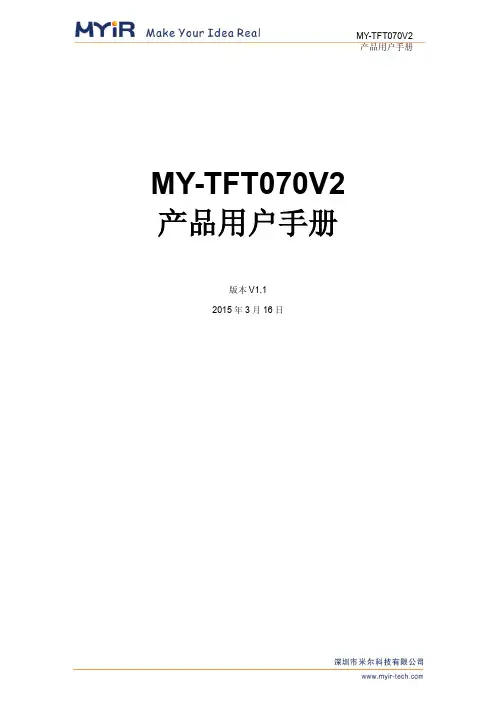
MY-TFT070V2 产品用户手册版本V1.12015年3月16日版本记录目录目录 (1)第1章产品概述 (2)1.1 产品简介 (2)1.2 规格参数 (2)1.3 产品预览 (3)第2章硬件指南 (5)2.1 引脚分布 (5)2.2 信号定义 (5)2.3 电气特性 (6)2.4 时序参数 (7)第3章机械参数 (10)附录 (12)附录一联系方式 (13)附录二售后服务与技术支持 (14)第1章产品概述1.1 产品简介MY-TFT070V2是深圳米尔科技有限公司推出的7寸液晶模块,是彩色有源矩阵薄膜晶体管(TFT)液晶显示器(LCD),由TFT LCD显示器件,连接件,控制与驱动外围电路,PCB驱动底板等组成,驱动底板预留1.27mm间距的IDC排线插针(25pinX2)和0.5mm 间距的FPC连接器两种连接方式,是专为米尔科技ARM主板设计的配套LCD液晶显示模块。
1.2 产品特性MY-TFT070V2兼容三种触摸输入方式,分别为电阻式触摸输入、电容式触摸输入和外置式输入,可以根据需要任意选用需要的方式,同时只能有一种触摸方式被连接。
图1-1MY-TFT070V2带有一颗存储芯片,用来保存LCD的一些常规信息,MYiR的开发板系统能够版识别MY-TFT070V2,并根据这些信息来加载相应的驱动。
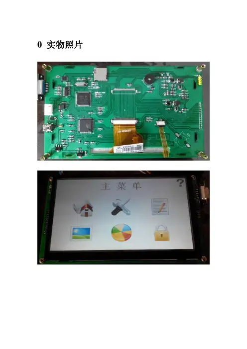
1.3 规格参数1.4 产品预览MY-TFT070V2 产品平面图如图1-2、图1-3所示:图1-2 MY-TFT070V2产品正面图图1-3 MY-TFT070V2 产品背面图第2章硬件指南2.1 接口分布底板接口分布如下图2-1所示:图2-1 底板接口分布图如上图所示,驱动底板预留1.27mm间距的50pin IDC排线插针(J1)和0.5mm间距的50pin FPC连接器(J2)两种连接方式,默认连接50pin IDC排线。
J4为电阻触摸信号连接,J5,J7分别为电容触摸控制信号连接,默认选择J5电容触摸模式。
1.77寸TFT使用说明外观美观大方,质量可靠,采用品牌厂商生产的TFT,提供多个例程,程序精炼、准确、实用。
您的满意就是我们的成功!TFT尺寸:1.7”;分辨率:128xBGRx160,可达262K色;电压类型:支持5V或3.3V电压输入,5v电压接入时,“VCC_SEL”(即16、17pin)断开;3.3v电压接入时,“VCC_SEL”短接;接口类型:支持8位数据接口或16位数据接口,8位数据接口可与12864液晶接口兼容(修改一下程序中的接口定义即可)。
使用16位数据接口时,“MOD”(即18pin)连接到GND。
兼容12864接口,TFT第一脚与12864接口第一脚对齐,注意12864接口的背光控制脚(第三脚)用跳帽连接到地(使TFT的CS控制信号为低电平)如果TFT仍显示不了则需将12864接口电位器旋转至GND。
TFT液晶各引脚功能说明如下:GND:接地;VCC:5V/3V电压输入,注意VCC_SEL的连接;CS:片选信号;RS:命令/数据选择;RS=0写数据,RS=1写命令;WR:写控制信号;RD:读控制信号;D8~D15: 使用8位数据口时为8位数据/命令并行口;使用16位数据/命令并行口时为其高8位;RST:液晶复位信号;VCC_SEL: 5v VCC接入时“VCC_SEL”断开;3.3v VCC接入时“VCC_SEL”短接;MOD: 数据/命令并行口的模式选择,MOD=GND时TFT为16位工作模式,MOD 不连接时TFT为8位工作模式;D0~D7:仅在使用16位数据/命令并行口时使用,为16位数据/命令并行口的低8位;液晶控制IC说明请参考“S6D0144.pdf”,液晶FPC接口定义请参考“GG1P0360管脚定义.pdf”。
8位接口模式,程序中的接口定义:D8~D15 = P0;CS = P2^1;RST = P2^2;RS = P2^5;WR_ = P2^4;RD_ = P2^3;16位接口模式,程序中的接口定义:D0~D7 = P0;D8~D15 = P1;CS = P2^1;RST = P2^2;RS = P2^5;WR_ = P2^4;RD_ = P2^3;SD卡使用方法程序4的功能是将SD卡中存储的图片显示到TFT,故此处SD卡主要用来存储图片。
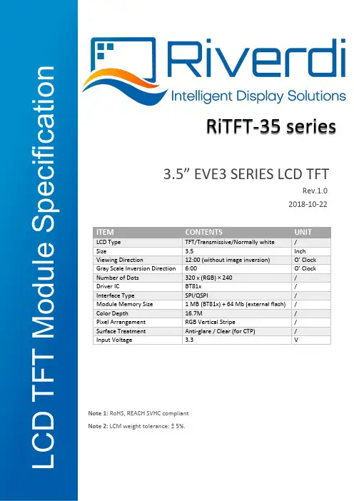
ITEMCONTENTSUNITLCD Type TFT/Transmissive/Normally white / Size3.5Inch Viewing Direction12:00 (without image inversion) O’ Clock Gray Scale Inversion Direction 6:00O’ Clock Number of Dots 320 x (RGB) × 240 / Driver ICBT81x / Interface TypeSPI/QSPI/ Module Memory Size 1 MB (BT81x) + 64 Mb (external flash) / Color Depth16.7M/ Pixel Arrangement RGB Vertical Stripe/ Surface Treatment Anti-glare / Clear (for CTP) / Input Voltage3.3V3.5” EVE3 SERIES LCD TFTRiTFT-35 seriesRev.1.0 2018-10-22L C D T F T M o d u l e S p e c i f i c a t i o nNote 1: RoHS, REACH SVHC compliant Note 2: LCM weight tolerance: ± 5%.CONTENTS (2)1 MODULE CLASSIFICATION INFORMATION (3)2 ASSEMBLY GUIDE - INTEGRATION (3)2.1 Mounting frame (4)3 MODULE DRAWING (4)4 ABSOLUTE MAXIMUM RATINGS (5)5 ELECTRICAL CHARACTERISTICS (5)6 BACKLIGHT CHARACTERISTICS (5)7 ELECTRO-OPTICAL CHARACTERISTICS (5)8 INTERFACE DESCRIPTION (7)9 BT8x CONTROLLER SPECIFICATIONS (8)9.1 Serial host interface (8)9.2 Block Diagram (8)9.3 Host interface SPI mode 0 (9)9.4 Backlight driver block diagram (9)10 LCD TIMING CHARACTERISTICS (9)10.1 Clock and data input time diagram (9)10.2 Parallel RGB timing table (11)11 TOUCH SCREEN PANEL SPECIFICATIONS (11)11.1 Electrical characteristics (11)11.1.1 For capacitive touch panel (11)11.1.2 For resistive touch panel (12)11.2 Mechanical characteristics (12)11.2.1 For capacitive touch panel (12)11.2.2 For resistive touch panel (13)12 INSPECTION (13)12.1 Inspection condition (13)12.2 Inspection standard (14)13 RELIABILITY TEST (17)14 LEGAL INFORMATION (18)1. BRAND RV – Riverdi2. PRODUCT TYPE T – TFT StandardF – TFT Custom3. DISPLAY SIZE 35– 3.5”4. MODEL SERIAL NO. A (A-Z)5. RESOLUTION H– 320x240 px6. INTERFACE B – TFT + Controller BT81x7. FRAME N – No FrameF – Mounting Frame8. BACKLIGHT TYPE W – LED White9. TOUCH PANEL N – No Touch PanelR – Resistive Touch Panel C – Capacitive Touch Panel10. VERSION 00(00-99)RiTFT-35-RES RVT35AHBNWR00 BT816, resistive touch panelRiTFT-35-CAP RVT35AHBNWC00 BT815, capacitive touch panelRiTFT-35-FR RVT35AHBFWN00 BT816, no touch panel, mounting frame RiTFT-35-RES-FR RVT35AHBFWR00 BT816, resistive touch panel, mounting frame RiTFT-35-CAP-FR RVT35AHBFWC00 BT815, capacitive touch panel, mounting frame2.1Mounting frameFor dimension s 3.5”, 4.3”, 5.0” and 7.0” the product with mounting frame version is available. Thanks to the four catches attached to the side, frame provides strong assembly to the surface by mounting element (like the screw, see Figure 3). The frames are specially designed to fit Riverdi products perfectly. The diameter of the mounting hole is 3.5mm.Figure 1. Mounting frameRiTFT-35 series3MODULE DRAWING `` RiTFT-35© 2018 Riverdi Page 4 of 24 RiTFT-35 seriesRiTFT-35-FR© 2018 Riverdi Page 5 of 24 RiTFT-35 seriesRiTFT-35-CAP© 2018 Riverdi Page 6 of 24 RiTFT-35-CAP-FR© 2018 Riverdi Page 7 of 24 RiTFT-35-RES© 2018 Riverdi Page 8 of 24 RiTFT-35-RES-FR© 2018 Riverdi Page 9 of 24 4ABSOLUTE MAXIMUM RATINGSPARAMETER SYMBOL MIN MAX UNITSupply Voltage for Logic VDD 0 4.0 V Supply Voltage for LED Inverter BLVDD 0 7.0 VInput Voltage for Logic VIN 0 4.0 VLED forward current (each LED) IF - 25 mA Operating Temperature T OP-20 70 °C PARAMETER SYMBOL MIN TYP MAX UNIT NOTES Supply Voltage For Module VDD 3.0 3.3 3.6 VInput Voltage for LED Inverter BLVDD 2.8 5.0 5.5 VLED Backlight Current IDD backlight- 150 187 mA BLVDD=3.3V LED Backlight Current IDD backlight- 93 117 mA BLVDD=5V Input Voltage ' H ' level V IH0.7VDD - VDD VInput Voltage ' L ' level V IL0 - 0.2VDD VInput Current I In TBD mAInput Current for module with CTP I InC TBD mAITEM SYMBOL MIN TYP MAX UNIT Voltage for LED backlight V l- 19.2 20.4 V Current for LED backlight I l- 20 25 mA LED Life Time - 30000 50000 - HrsLNote 1. Contrast Ratio(CR) is defined mathematically as below, for more information see Figure .Contrast Ratio =Average Surface Luminance with all white pixels (P1,P2,P3,P4,P5) Average Surface Luminance with all black pixels (P1,P2,P3,P4,P5)Note 2. Surface luminance is the LCD surface from the surface with all pixels displaying white. For more information, see Figure .Lv = Average Surface Luminance with all white pixels (P1, P2, P3, P4, P5)Note 3.The uniformity in surface luminance δ WHITE is determined by measuring luminance at each test position 1 through 5, and then dividing the maximum luminance of 5 points luminance by minimum luminance of 5 points luminance. For more information, see Figure .δ WHITE =Minimum Surface Luminance with all white pixels (P1,P2,P3,P4,P5) Maximum Surface Luminance with all white pixels (P1,P2,P3,P4,P5)Note 4. Response time is the time required for the display to transition from white to black (Rise Time, Tr) and from black to white (Decay Time, Tf). For additional information see FIG 1. The test equipment is Autronic-Melchers’s ConoScope series.Note 5.CIE (x, y) chromaticity, the x, y value is determined by measuring luminance at each test position 1 through 5, and then make average value.Note 6. Viewing angle is the angle at which the contrast ratio is greater than 2. For TFT module the contrast ratio is greater than 10. The angles are determined for the horizontal or x axis and the vertical or y axis with respect to the z axis which is normal to the LCD surface. For more information see Figure .Note 7. For viewing angle and response time testing, the testing data is based on Autronic-Melchers’s ConoScope series. Instruments for Contrast Ratio, Surface Luminance, Luminance Uniformity, CIE the test data is based on TOPCON’s BM-5 photo detector.Note 8. For TFT module, Gray scale reverse occurs in the direction of panel viewing angle.Figure 2. The definition of response timeFigure 3. Measuring method for Contrast ratio, surface luminance, Luminance uniformity, CIE (x, y) chromaticityFigure 4.The definition of viewing angle8INTERFACE DESCRIPTION9BT8x CONTROLLER SPECIFICATIONSBT8x or EVE3 (Embedded Video Engine 3) simplifies the system architecture for advanced human machine interfaces (HMIs) by providing functionality for display, audio, and touch as well as an object oriented architecture approach that extends from display creation to the rendering of the graphics.9.1Serial host interfaceFigure 5.SPI interface connection Figure 6. QSPI interface connectionSPI Interface– the SPI slave interface operates up to 30MHz.Only SPI mode 0 is supported. The SPI interface is selected by default (MODE pin is internally pulled low by 47k resistor).9.2Block DiagramFigure 7.. BT8x Block diagram9.3Host interface SPI mode 0Figure 8. SPI timing diagramFor more information about BT8x controller please go to official BT8x website.https:///Products/ICs/BT81X.html9.4Backlight driver block diagramBacklight enable signal is internally connected to BT8x Backlight control pin. This pin is controlled by two BT8x’s registers. One of them specifies the PWM output frequency, second one specifies the duty cycle. Refer to BT8x datasheet for more information.Figure 9. Backlight driver block diagram10LCD TIMING CHARACTERISTICS10.1Clock and data input time diagramFigure 10. DE mode timing diagramBT8xFigure 11. SYNC mode timing diagramFigure 12. Timing diagram10.2Parallel RGB timing tableTiming parameter (VDD=3.3V, GND=0V, Ta=25˚C)PARAMETER SYMBOL MIN TYP MAX UNIT CONDITION CLK Clock Time T clk 1/Max(F CLK) - 1/Min(F CLK) ns -11TOUCH SCREEN PANEL SPECIFICATIONS11.1Electrical characteristicsNote: Avoid operating with hard or sharp material such as a ball point pen or a mechanical pencil except a polyacetal pen (tip R0.8mm or less) or a fingerITEM VALUE UNIT REMARKMin. Typ. Max.Linearity - - 1.5 % Analog X and Y directions Terminal Resistance 200 - 900 ΩX100 - 600 ΩY11.2Mechanical characteristicsNote 1: Force test condition, Input DC 5V on X direction, Drop off Polyacetal Stylus (R0.8), until output voltage stabilize, then get the R8.0mm Silicon rubber and do finger Activation force test. Next step, 9 points.Note 2: Measurement surface area conditions, Scratch 100,000 times straight line on the film with a stylus change every 20,000 times with Force: 250gf, Speed: 60mm/sec by R0.8 polaceteal stylus.Note 3: Pitting test, Pit 1, 000, 000 times on the film with R0.8 silicon rubber with Force: 250gf and Speed: 2 times/sec.Note 1: Force test condition, Input DC 5V on X direction, drop off Polyacetal Stylus (R0.8), until output voltage stabilize, then get the R8.0mm Silicon rubber and do finger Activation force test. Next step, 9 points.ITEM VALUE UNIT REMARKMin. Typ. Max.12INSPECTIONStandard acceptance/rejection criteria for TFT module.12.1Inspection conditionAmbient conditions:•Temperature: 25±°C•Humidity: (60±10) %RH•Illumination: Single fluorescent lamp non-directive (300 to 700 lux)Viewing distance:35±5cm between inspector bare eye and LCD.Viewing Angle:U/D: 45°/45°, L/R 45°/45°12.2Inspection standard Item Criterion Black spots, whitespots, light leakage,Foreign Particle(round Type)D=(x+y)2*Spots density: 10 mmSize < 5”Average Diameter Qualified QtyD < 0.2 mm Ignored0.2 mm < D < 0.3 mm 30.3 mm < D < 0.5 mm 20.5 mm < D 0Size >= 5”Average Diameter Qualified Qty D<0.2 mm Ignored0.2 mm < D < 0.3 mm 40.3 mm < D < 0.5 mm 20.5 mm < D 0Clear spotsSize >= 5”Average Diameter Qualified Qty D<0.2 mmIgnored 0.2 mm < D < 0.3 mm 4 0.3 mm < D < 0.5 mm 2 0.5 mm < D*Spots density: 10 mm Size < 5”Average Diameter Qualified Qty D < 0.2 mmIgnored 0.2 mm < D < 0.3 mm 3 0.3 mm < D < 0.5 mm 2 0.5 mm < D 0Polarizer bubblesSize < 5”Average Diameter Qualified Qty D < 0.2 mmIgnored 0.2 mm < D < 0.5 mm 3 0.5 mm < D < 1 mm 2 1 mm < D 0 Total Q’ty 3Size >= 5”Average Diameter Qualified Qty D<0.25 mmIgnored 0.25 mm < D < 0.5 mm 3 0.5 mm < D 0Electrical Dot DefectSize < 5”itemQualified Qty Black do defect 4 Bright dot defect 2 Total Dot 5Size >= 5”itemQualified Qty Black do defect 5 Bright dot defect 2 Total Dot 5Touch panel spotSize < 5”Average Diameter Qualified QtyD < 0.2 mm Ignored0.2 mm < D < 0.4 mm 50.4 mm < D < 0.5 mm 213RELIABILITY TESTNO. TEST ITEM TEST CONDITION REMARKS1 High Temperature Storage 80±2°C/240hours Note 22 Low Temperature Storage -30±2°C/240hours Note 1,2Note 1: Without water condensation.Note 2:The function test shall be conducted after 2 hours storage at the room temperature and humidity after removed from the test chamber.14LEGAL INFORMATIONRiverdi makes no warranty, either expressed or implied with respect to any product, and specifically disclaims all other warranties, including, without limitation, warranties for merchantability, non-infringement and fitness for any particular purpose. Information about device are the property of Riverdi and may be the subject of patents pending or granted. It is not allowed to copy or disclosed this document without prior written permission.Riverdi endeavors to ensure that the all contained information in this document are correct but does not accept liability for any error or omission. Riverdi products are in developing process and published information may be not up to date. Riverdi reserves the right to update and makes changes to Specifications or written material without prior notice at any time. It is important to check the current position with Riverdi.Images and graphics used in this document are only for illustrative the purpose. All images and graphics are possible to be displayed on the range products of Riverdi, however the quality may vary. Riverdi is no liable to the buyer or to any third part for any indirect, incidental, special, consequential, punitive or exemplary damages (including without limitation lost profits, lost savings, or loss of business opportunity) relating to any product, service provided or to be provided by Riverdi, or the use or inability to use the same, even if Riverdi has been advised of the possibility of such damages.Riverdi products are not fault tolerant nor designed, manufactured or intended for use or resale as on line control equipment in hazardous environments requiring fail – safe performance, such as in the operation of nuclear facilities, aircraft navigation or communication systems, air traffic control, direct life support machines or weapons systems in which the failure of the product could lead directly to death, personal injury or severe physical or environmental damage (‘High Risk Activities’). Riverdi and its suppliers specifically disclaim any expressed or implied warranty of fitness for High Risk Activities. Using Riverdi products and devices in 'High Risk Activities' and in any other application is entirely at the buyer’s risk, and the buyer agrees to defend, indemnify and hold harmless Riverdi from any and all damages, claims or expenses resulting from such use. No licenses are conveyed, implicitly or otherwise, under any Riverdi intellectual property rights.。
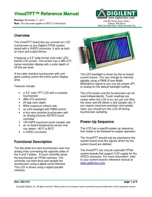
TFT触摸屏使用说明2一、.4寸TFT 触摸屏使用说明要正确使用TFT 触摸屏,需要借助相应的单片机实验板,这里,以顶顶电子开发板DD-900实验开发板为例进行介绍,值得庆幸的是,DD-900上设有3V 电压输出端,因此,可以方便地为TFT 触摸屏供电。
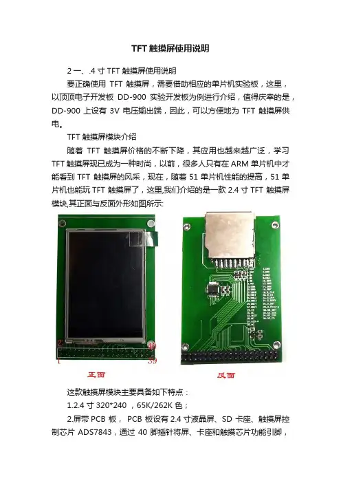
TFT 触摸屏模块介绍随着TFT 触摸屏价格的不断下降,其应用也越来越广泛,学习TFT 触摸屏现已成为一种时尚,以前,很多人只有在ARM 单片机中才能看到TFT 触摸屏的风采,现在,随着51单片机性能的提高,51单片机也能玩TFT 触摸屏了,这里,我们介绍的是一款2.4寸TFT 触摸屏模块,其正面与反面外形如图所示:这款触摸屏模块主要具备如下特点:1.2.4寸320*240 ,65K/262K 色;2.屏带PCB 板, PCB 板设有2.4寸液晶屏、SD 卡座、触摸屏控制芯片ADS7843,通过40脚插针将屏、卡座和触摸芯片功能引脚,引脚间距为2.54mm ,采用杜邦线可十分方便地与单片机进行连接。
PCB 引出脚排列及功能如图所示:3.屏设置为8位,用户也可根据实际情况设置为16位。
4.控制IC 为ILI9325。
二、供电及连接说明DD-900实验开发板采用的是5V 供电,因此,单片机应采用5V 单片机,如STC89C516RD+、STC12C5A60S2等,晶振采用30M ,注意TFT 要采用3V 供电,否则有可能烧屏,TFT 与单片机连接时可加限流电阻,电阻大小为470欧左右,也可以不加,但单片机不可设置为推挽模式,各引脚连接如下: TFT 触摸屏 DD-900实验开发板说明GND GND 屏与背光供电VCC 3V LED+ 3V DB8~DB15 P00~P07 液晶屏部分DB0~DB7不连接(这里采用是8位方式,不用连接)RS P26 WR P25 RD P24 CS P27 RES P23 D_CLK P21 触摸控制部分D_CS P20 D_DIN P22 D_BUSY P34 D_DOUT P33 D_Penirq (中断) P35 SD_OUT 根据程序进行定义 SD 卡座部分(前两个实验,此部分未采用) SD_SCK 根据程序进行定义SD_DIN根据程序进行定义SD_CS 根据程序进行定义注意:在TFT 的PCB 板上标有TFT 的引脚功能,一定要认清管脚与标注的对应关系。
![7[1].0寸TFT模块详细说明书](https://uimg.taocdn.com/03b98002bed5b9f3f90f1ca0.webp)
NHC_36彩色液晶显示控制模块使用说明一、N HC_36型显示控制模块的特点。
A:安装方便,板尺寸为168mm╳116mm,安装孔Ф3mm,四个安装孔位置为162mm╳110mm,高度为14mm。
B:微处理器可以随时读写显示存储器,而不影响显示效果,即显示不会出现“雪花”。
C:与微处理器接口连接简单,接口的读、写操作兼容8031总线时序。
D:有两页显示缓存,可以任意设定显示页和操作页。
二、物理特性:三、电器参数:NOTE1:最小电流的条件是电源4.8V,不对模块操作,液晶屏幕显示全黑。
最大电流的条件是电源5.2V,对控制卡进行高速逻辑写操作,屏幕显示全白。
四、MCU接口定义用户板和NHC_36控制模块的连接(J1)采用21线2.54mm间距单排插针。
对液晶的操作采用标准intel总线时序(8031总线时序)。
管脚图如下:(顶视图)如果第18管脚“RD\”不用时,接上拉电阻五、NHC_36液晶控制板与微处理器的接口时序接口时序与8031的总线时序相同时序:A0、A1/WR、D7—D0(D7—D0(READ时序特性参数六、指令介绍及编程方法:CS WR RD A1 A0 D0-D7H 任意任意任意任意操作无效L L H 0 0 写显示数据到LCDL H L 0 0 从LCD读数据L L H 0 1 写显示数据前用:设定行地址,地址0-233对应液晶屏从上到下1到234行L L H 1 0 设定列地址(0-479)L L H 1 1 设定显示页和操作页1.写指令和数据a)设定显示页和操作页地址。
(A1=A0=1,CS=0,WR=0)开机时先执行此操作再执行其他操作,工作中不需要换页时D4位设定操作页。
D0位设定显示页。
b)写行地址。
(A1=0,A0=1)c)写列地址高字节。
(A1=1,A0=0)d)写列地址低字节。
(A1=1,A0=0)e)写1个字节数据。
对应一个象素点。
(A1=0,A0=0)R2、R1、R0表示红色灰度,从000到111,灰度有8级R2为高灰度位,R0为低灰度位。
4inch TFT Touch ShieldUser ManualOVERVIEWThis is a 4inch resistive screen TFT LCD, 320x480 resolution, integrate controller on board. It uses SPI interface, can be used to display image, text or draw geometric figure with functions.STM32 and Arduino examples are provided for easy porting.PARAMETERSLCD Type: TFTLCD Interface: SPILCD Controller: ILI9486Touch Screen Controller: XPT2046Touch Screen Type: ResistiveResolution: 320x480 (Pixel)Color Gradation Exponent: 65536INTERFACESymbol Arduino PIN STM32 PIN Description 5V 5V 5V 5V power inputGND GND GND GroundSCLK D13 PA5 SPI clockMISO D12 PA6 SPI data inputMOSI D11 PA7 SPI data outputLCD_CS D10 PB6 LCD chip selectLCD_BL D9 PC7 LCD back lightLCD_RST D8 PA9 LCD resetLCD_DC D7 PA8 LCD data/commandselectionHOW TO USEHARDWARE CONFIGURATION•If there is ICSP interface on Arduino board, set the SPI Config switch onto ICSP position.(default)•If Arduino board has no ICSP interface, set the SPI Config switch onto the position that SCLK\D13, MISO\D12, MOSI\D11EXAMPLESWe provide Arduino UNO examples and XNUCLEO-F103RB examples for this screen.ARDUINO EXAMPLES1.Download the examples: 4inch TFT Touch Shield code.7z, and copy the libraries which are inArduino\lib folder of examples to the libraries folder which is under the installation directory of Arduino IDE.2.Before running the LCD_ShowBMP code, copy the pictures which is in the PIC folder to SDcard.3.Open the LCD_ShowBMP project with Arduino IDE, download to Arduino board.4.The Touch code use four sets of calibration values, could support painting operation in fourdirections. There are five colors which could be selected on the right. The size of paintbrush is 9 pixels by default. Users can also click the AD on screen to calibrate:Please use the stylus click the cross on the screen. The cross will always move until thescreen adjustment is completed.5.Following the prompt, click the red sign “+” one by one to finish the calibration.STM32 EXAMPLES1.Before running the code that display image. copy the pictures which is in the PIC folder toSD card. Then insert the LCD to NUCLEO or XNUCLEO board.2.Open the project with MDK, download to the NUCLEO or XNUCLEO development board.3.The LCD will first show some common functions: Draw dots, draw dotted line and solid line,rectangle, filled rectangle, circle and solid circle. Every figure keeps for 3s. You can change the size of dot, the width of lines and the size of the circles.4.The Touch code use four sets of calibration values, could support painting operation in fourdirections. There are five colors which could be selected on the right. The size of paintbrush is 9 pixels by default. Users can also click the AD on screen to calibrate:Please use the stylus click the cross on the screen. The cross will always move until thescreen adjustment is completed.5.Following the prompt, click the red “+” one by one to finish the calibration.Note:Image: 320x480, 24bit, bmp.SD card: FAT。
墙式3.2寸液晶触摸屏使用说明书一.技术参数:✧屏幕显示: 3.2寸TFT真彩矩阵。
✧触摸屏面板四线电阻式。
✧颜色深度:65M - 16bits。
✧分辨率:320 x 240 Pixel。
✧可视角度:100° 垂直100° 水平倾斜角度:30°。
✧通讯方式:RS-485标准串行总线,通讯速率:1200~256000 bps可设,长度:8 bits,奇偶校验:无,停止位 1✧内存:1M bytes (系统资源760K,用户240K)。
✧接口:1个5Pin接线座✧工作电源:DC12V--DC24V。
✧功耗:工作状态从100 mA –睡眠状态为40 mA 。
✧外壳:面板:锌合金底盒:阻燃ABS。
✧工作温度:0℃至50℃ 。
✧储存温度:-10℃~60℃。
✧周围湿度:20~90% RH (无结露)。
✧安装底盒:标准86底盒✧尺寸(mm) 117(L) x 100(W) x 32(D)。
颜色:多色可换面板。
二.墙式3.2寸触摸屏功能:1. 3.2寸触摸彩屏显示。
2.可设置1到10个按键3.每个按键可以自定义发送代码4.可自己设计界面样式5.通讯方式:标准的485通讯方式,波特率可变。
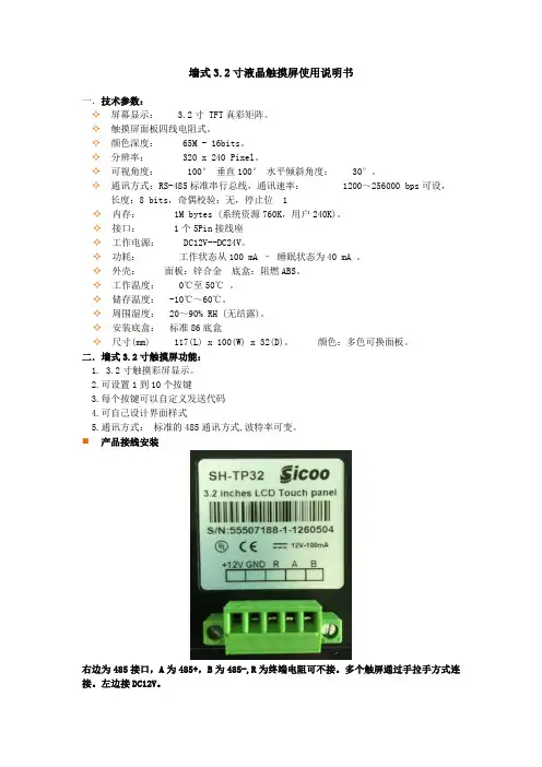
⏹产品接线安装右边为485接口,A为485+,B为485-,R为终端电阻可不接。
多个触屏通过手拉手方式连接。
左边接DC12V。
三.软件设置●配置软件是为配合3.2触屏进行系统配置而开发的一个应用工具,仅适用于(SH-TP32系列产品)。
●到下载SH-TP32配置软件,软件为纯绿色软件,无需安装。
直接复制到硬盘中双击即可运行。
●参照本说明书“产品接线”,通过USB转485配置线与触屏接通,同时将触屏上电。
运行软件,导入背景和按键后即可进入上传。
3.1 软件使用注意:在写入程序时ID要与写入的触屏一致。
长按触屏8秒,触屏会进入工程模式,此时就可修改触屏ID、屏幕保护、代码发送间隔时间。
● 3.1.2 “文件”菜单打开配置:打开前期保存在电脑的工程文件保存配置:把编辑好的按键界面保存在电脑里写入配置:把当前界面写入SH-TP32(写入后,触屏会自动重启)。

2.4寸TFT使用说明一、编译程序说明打开TFT屏的测试程序中的main.c文件,看程序中上部分的宏定义:这里是选择执行哪种测试程序,分别为:1. 普通测试(文字和字符)2. 显示图片(全屏的组合图片)3. 触摸屏手写测试4. 从SD卡中读取图片将Test_Mode 定义成上面4种不同的值,再编译,就会编译出相应的测试程序比如要执行SD卡测试,第36行就写为:#define Test_Mode SD_SHOWPIC二、接口连接说明SD卡接口连接顺序:CS Æ P1.4MOSI Æ P1.5MISO Æ P1.6CLK Æ P1.7也可以使用开发板上TF卡接口,接口顺序不变,无需连线触摸屏接口连接顺序:DCLK Æ P1.5CS Æ P1.4DIN Æ P1.3BUSY Æ P1.2DOUT Æ P1.1IRQ Æ P1.0如果需要修改管脚定义,打开头文件“STC_NEW_8051.h”,修改相应的管脚,如下图:三、 SD卡读取图片显示说明1. 首先要格式化你的SD卡,文件系统选择FAT格式2. 使用Image2LCD软件将图片转换成BIN类型,按照如下配置将生成的.bin文件存放到SD卡中3.打开WINHEX软件,按如下步骤打开SD卡:4. 选中刚刚放入的.bin文件,查看“Offset”下方的第一个地址即为该图片文件的起始地址:5. 修改程序中的图片起始地址变量:6. 编译程序,下载到开发板中运行程序先初始化SD卡,显示“SD Card Init, Please wait...”如果初始化失败,显示“SD Reset error”和“SD Reset error”,程序中止。
需要检查SD卡是否插入插槽中,接线是否连接正确如果初始化成功,显示“SD Reset success!”和“SD Init success!”随后便会开始刷屏。
2.4寸TFT彩屏使用说明书彩屏驱动IC:ILI9325实验板:LY-51S实验板编写:侯瑞阳2013年01月一、彩屏模块简介屏幕尺寸:2.4寸TFT彩屏分辨率:320x240 262K色接口类型:8位数据接口,接口兼容12864液晶接口,①脚对齐电源类型:5V电源接口,板上有3.3V稳压芯片,不需要电平转换SD卡模式:SPI模式触摸IC:XPT2046图1-1 2.4寸TFT彩屏模块二、彩屏结构组成及原理TFT屏(Thin Film Transistor)是薄膜晶体管型液晶显示屏,它的每一个象素点都是由集成在其后的薄膜晶体管来驱动的,这样不仅提高了显示屏的响应速度,同时可以精确控制显示色阶,所以TFT液晶的色彩更逼真。
TFT屏主要的构成包括:背光源、导光板、偏光板、滤光板、玻璃基板、配向膜、液晶材料、薄膜晶体管等。
图2-1 彩屏的基本结构图2-2 TFT彩屏内部结构TFT液晶模块可以显示数字、中英文字符和图案。
彩色,图案分辨率较高。
由于TFT显示器成本日渐降低,并且人们越来越渴望拥有用户友好程度更高的图形界面,因此有越来越多的工程师把TFT显示器设计到他们的产品中去。
TFT模块尺寸指屏幕的对角线长度。
常用有:1.6、1.8、2.0、2.2、2.4 、2.6、2.8、3.0、3.2、3.4、3.6、4、4.3、5.7 、8.4 、10.4 、15 、17 、19 、21 英寸等。
屏幕高宽比小尺寸TFT模块一般是3:4,大尺寸的也有16:9的。
分辨率指水平像素和垂直像素的数量。
三、学习彩屏的准备知识1、什么是图形和图像图形:如一段直线,在单片机内存储时只需要存储起点X、Y坐标和终点X、Y 坐标,存储量极小,但在显示器上显示时,和图像的显示是一致的,也是通过像素点的组合来显示的。
图3-1 像素点组成图形图像:如一张人物照片,在单片机内存储时需要存储所有像素点的信息,存储量极大,在显示器上显示时,通过像素点的点阵组合来完成显示的图3-2 像素点组成图像2、什么是像素像素:图像的最小组成单位。
4.3寸TFT显示器 SM.04TL/C使用手册出版状态:标准产品版本: V1.0上海新时达电气股份有限公司版权所有,保留一切权利在没有得到本公司许可时,任何单位和个人不得擅自摘抄、复制本书(软件等)的一部分或全部,不得以任何形式(包括资料和出版物)进行传播。
版权所有,侵权必究。
内容如有改动,恕不另行通知。
Copyright© by Shanghai STEP Electric Co., Ltd.All rights reservedThe information in this document is subject to change without notice . No partof this document may in any form or by any means(electronic,mechanical,micro-coping,photocopying,recording or otherwise)be reproduced,stored in a retrival system or transmitted without prior writtenpermission from Shanghai STEP Electric Corporation一、外形图片及尺寸图1 4.3寸TFT显示器外形图(竖显和横显)图2 4.3寸TFT显示器尺寸(mm)二、功能特点1、适用于新时达串行通讯系统;2、采用4.3寸TFT作为显示界面,真彩色显示(16位色),分辨率为480×272;3、能够显示电梯楼层、运行方向和背景图片;4、显示内容均存储在显示器内,可通过USB端口对其进行更新;5、即可做横显,也可以做竖显,通过拨码开关设置;6、显示界面尺寸:97mm×55mm。
三、端口定义图3 SM.04TL/C端子端子定义如下表所示:端子号端子定义插座型号插头型号JP1 电源与通讯 S4B-XH-A XHP-4JP2 上召按钮接口CH2510-4AW CH2510-4YJP3 下召按钮接口JP4 锁梯JP1为电源和通讯线接口,其接线示意图如图4所示:图4 电源和通讯接线示意图JP2、JP3和JP4的1脚和2脚接按钮灯,3脚和4脚接按钮的输入,如图5所示:图5 按钮接线示意图拨码开关说明如下:序号位号功能SW1.1 拨到“ON”,进入楼层设置状态,用于设置当前楼层,按上召按钮楼层值增加,按下召按钮楼层值减少,设置完毕后将其拨到“OFF”状态。
使用说明书TFT仪表操作说明目录1. 目录 (1)2. TFT仪表操作说明 (2)按键功能 (2)3. 互联页面 (4)4. MOTOFUN下载方式 (5)应用市场下载 (5)扫描屏幕二维码下载 (5)APP使用权限 (5)5. APP防止误杀和被杀方法(安卓) (7)6. MOTOFUN 手机投屏 (8)手机互联操作步骤(安卓) (8)手机互联操作步骤(iphone) (10)7. MOTOFUN 来电显示 (11)MOTOFUN 数据,消息显示 (12)蓝牙数据链接注意事项 (13)8. MOTOFUN 操作说明 (14)1.开机:2.开机动画:开机过程:仪表开机,显示开机Logo 开机动画,刻度及LED 全显示点亮3.开机静止画面:4. 开机静止画面白天模式画面:白底黑字(控制光敏传感器) 黑夜模式画面:黑底白字(控制光敏传感器)5.按键功能描述:界面切换:操作逻辑:1. 在TOTAL 模式下,长按S 键2秒进入设置页面2. 单击M 键循环选择3. 单击S 键确认进入设置选项,选中即可生效4. 长按M键返回上一级 1. 单击M 键循环选择 2. 单击S 键确认进入设置选项, 选中即可生效3. 如果有3个界面,缩略图片 变成3个时钟设置操作逻辑:1. 单击M 键循环选择AM 或PM, 选中即生效2. 单击S 键切换到小时位置,时钟 进入可以调节状态,再单击M 键累加3.再次单击S 键移位到分钟位置,分钟进入可以调节状态,单击M 键累加4.长按M 键返回上一级单位设置操作逻辑: 1. 单击S 键循环选择公制或英制, 选中即生效2. 长按M键返回上一级语言设置操作逻辑: 1. 单击S 键循环选择中文或英文, 选中即生效2. 长按M 键返回上一级车辆信息操作逻辑:1. 进入车辆信息,显示车辆软件 版本及设备标识2. 长按M 键返回上一级3.互联页面1.APP中使用扫码连接,对此二维码进行互联2.经典蓝牙:连接手机系统内部的蓝牙,进行电话通信, 在手机系统的设置中进行连接3.BLE蓝牙:通过MOTOFUN APP中蓝牙连接,进行蓝牙通信包括:微信电话或者是车身数据上传 (可以通过微信扫码二维码在浏览器中打开下载相应的APP)1.应用市场下载:在国内的安卓应用市场搜索:“MOTOFUN”,下载安装即可2.扫描屏幕二维码下载:通过浏览器或者微信,扫描屏幕二维码,在浏览器中打开下载APPAPP 使用权限1(安卓)安卓手机:首次安装MOTOFUN 会提示较多的权限需求,请均选择同意。
TFT LCD COLORMONITOR OPERATION MANUALMode 1Mode 2Mode 3DEAR CUSTOMERSThanks you for purchasing 8”TFT COLOR MONITOR,We hope that you will have the enjoyment of your new mini color TFT LCD.SAFEGUARDS AND PRECAUTIONS1、Please adopt the matched home AC power adapter.2、Do not remove the rear panel of this product. If in need of service, please call aqualified technician.3、Keep away form strong light while using this product so as to obtain theclearest and the most colorful picture.4、Do not seriously impact or drop the product onto the ground.5、Don’t use chemical solutions to clean this TFT LCD set.Please simply wipe witha clean soft cloth to keep the brightness of the surface.CONTENTS1 FEATURE-----------------------------------------------2 CONNECTION-----------------------------------------3 REMOTE CONTROLLER----------------------------4 MENU OPERATION-----------------------------------5 PARAMETER-------------------------------------------6 ACCESSORIES-----------------------------------------7 TROUBLE SHOOTING-------------------------------1、 FEATURE1、Mode 1131. POWER.:ON/OFF2. Indication Light for power supply: Red light means stand by ,Green lightmeans to work.3. PC/A V:VGA , A V switch.4. :Program selection key or using to select function in OSD.5. :Program selection key or using to select function in OSD.6. IR Sensor7. MENU:Display MENU key;8. VOL+: V olume up or using to adjust the number of selected function in OSD.9. VOL-: V olume down or using to adjust the number of selected function inOSD.10. 14P SKS cable input jack11. 12V power input jack12. Folding Bracket13. Touch penMode 2101.-:V olume down key or used to move cursor down in OSD mode2.+:V olume up key or used to move the cursor up in OSD mode3.<:Program selection key or used to select function in OSD mode4.M/E:Display MENU key5.>:Program selection key or used to select function in OSD mode6.A/V:VGA, A V switch7.POWER:ON/OFF8.14P SKS input jack9. DC 12V input jack10. Touch penMode 31011129 8 7 6 5 4 3 2 11. Indication Light for power supply: Red light means stand by ,Green light meansto work.2. VOL+: V olume up key or used to move cursor down in OSD mode3.VOL-: V olume down key or used to move the cursor up in OSD mode4.>: Program selection key or used to select function in OSD mode5.MENU:Display MENU key6.< : Program selection key or used to select function in OSD mode7.A/V: VGA, A V switch8.POWER:ON/OFF9.IR Sensor10.DC 12V input jack11.14P SKS input jack12. Touch pen2. CONNECTIONMode 1Mode 2& Mode 33、REMOTE CONTROLLER: MUTE: To activate OSD menu: V olume up or to adjust the value of setting function: To select function on OSD~: Unit, double-digit, three-Picture, no use.: NO USE4、MENU OPERATIONAfter connected correctly and then Power on, Press “MENU” on the unit or by remote control to show MENUIN A V MODEPress “</>”on the unit or “” on the remote control to select item, eg. ,and it will be highlighted; and then press +/ - of the unit or to adjust the favorite values. It shows current picture format (NTSC&PAL) below the dialog box.BRIGHTNESS: to adjust the luminance of brightnessSATURATION: to adjust the level of saturationTINT: to adjust the hue of imageLANGUAGE:There are 2 languages provided for choice, English and ChineseRESET: you can reset adjustment of the unit when click “YES”OSD H-POSITION ADJUSTMENT: to adjust the OSD move in horizontal directionOSD V-POSITION ADJUSTMENT: to adjust the OSD move in vertical directionOSD DURATION: to adjust the duration of OSD from5-100seconds.picture over-turn to left or rightpicture over-turn to up or downEXIT OSD: select “YES” to exitIN PC MODE:Press “</>”on the unit or “” on the remote control to select item, eg. ,and it will be highlighted with yellow; and then press +/ - of the unit or to adjust the favorite values. It shows picture mode specifications below the dialog box.BRIGHTNESS: to adjust the luminance of brightnessPHASE:to adjust the beginning point and terminal point of imageFREQUENCY: to adjust the frequency range of imageOSD H-POSITION:to adjust the picture position in horizontal directionOSD H-POSITION:to adjust the picture position in vertical directionRESET: you can reset adjustment of the unit when click “YES”COLOR TEMPERATURE:choose color and temperature at first, such as: 65000 K, 75000 K or 93000 K.Only if under “USER” mode, can adjust RED, GREEN and BLUE to meet the color value you need.LANGUAGE:There are 2 languages provided for choice, English and ChineseMISCELLANEOUS:to select to enter next pageAs follows:EXIT OSD: select “YES” to exitOSD H-POSITION ADJUSTMENT: to adjust the OSD move in horizontal directionOSD V-POSITION ADJUSTMENT: to adjust the OSD move in vertical directionOSD DURATION: to adjust the duration of OSD from5-100seconds.OSD AUTO COLOR:If select “YES” it will adjust automatic color system to the bestpicture over-turn to left or rightpicture over-turn to up or down5、PARAMETERTFT LCD SCREENTFT LCD (8 inch)High Resolutions 800*600Average Brightness250 cd/㎡Contrast Ratio 500: 1Mode 1 & Mode 2 4:3Aspect RatioMode 3 16:9Mode 1& Mode 2 140°/120° (H/V)Viewing AngleMode 3 130°/110° (H/V)Color System PAL-4.43 NTSC-3.58Power consumption ≤8.5WAudio Output ≤1.2WInput V oltage DC11-13VMode1 205L×178W×67H mm(Folding)205 L×150 W×210 H mm(Unfolding)Mode 2 220 x166 x37.5 mmDimensionMode 3 196×116×32.5(mm)Mode 1 WITH TOUCH 1024gWITHOUT TOUCH 945gMode2 WITH TOUCH 526gWITHOUT TOUCH 588gWeightMode 3 WITH TOUCH 610gWITHOUT TOUCH 518g6、ACCESSORIES1 2 3 4 5 61 VGA signal cable with 9 holes 1piece2 14P SKS patch cord of A/V cable 1piece3 DC adapter 1piece4 Remote controller 1piece5 Driver disk(Matched with touch function)1piece6 Operation manual 1copy7、TROUBLE SHOOTING7.1、A V MODE7.2、PC MODE① Image excursionAccording to the operation of image station adjustments to adjust: A. Press“<”key, select automatic functionB. Manual adjust as per the operation manual in the menu.C. Select correct refurbish and resolution rate Lose colorPlease check the VGA cable if connect correctly, or what is matter with the VGA cable, if any bend or break in cable, please adopt new VGA cable. No pictureA 、After connecting the power, the indicator light will turn red, thenpress“POWER” button, the unit will work, if the screen display “NO SIGNAL”, that is to say no signal input, at this time, you should open your computer; if the screen display “OVERRANGE”, that is to say signal mode input exceed the range of display, please adjust the refurbish rate of unit.B 、If the green light on the monitor is turned on, the management mode of the power is activated. You may press any key on the computer to activate it. The power of the monitor also has the management mode. If no effect after pressing the keyboard of the PC ,please press “POWER” key on the monitor.C 、If the indicator light is turned off, please check the power connection.Case(condition)Possible causesOnly black and white picture1. The number of “color” function on Video menu is zero.2. The present program have only black and white image. No picture 1. Check power connectin(check the working indicatorlight).2. Check if the A V cable is connected well.The remote controller can not work or insensitive 1. Check battery install method. 2. The battery is used out.3.The signal are influencedNo clear or really image, shaky picturePlease select correct resolution rate, renew the refurbish rate.If any questions, you may be contact with the related dealers.If the whole screen turn light, please check computer refurbish rate is less than 72Hz.Remark:* If happen image interruptive, it is possible that the VGA signal frequency is not matched with normal standard.* It is a normal condition that some bright lines appear on the screen when you are closed the unit.*To ensure a longer use, please make power management function of PC active.。
2一、.4寸TFT 触摸屏使用说明
要正确使用TFT 触摸屏,需要借助相应的单片机实验板,这里,以顶顶电子开发板DD-900实验开发板为例进行介绍,值得庆幸的是,DD-900上设有3V 电压输出端,因此,可以方便地为TFT 触摸屏供电。
TFT 触摸屏模块介绍
随着TFT 触摸屏价格的不断下降,其应用也越来越广泛,学习TFT 触摸屏现已成为一种时尚,以前,很多人只有在ARM 单片机中才能看到TFT 触摸屏的风采,现在,随着51单片机性能的提高,51单片机也能玩TFT 触摸屏了,这里,我们介绍的是一款2.4寸TFT 触摸屏模块,其正面与反面外形如图所示:
这款触摸屏模块主要具备如下特点:
1.2.4寸320*240 ,65K/262K 色;
2.屏带PCB 板, PCB 板设有2.4寸液晶屏、SD 卡座、触摸屏控制芯片ADS7843,通过40脚插针将屏、卡座和触摸芯片功能引脚,引脚间距为2.54mm ,采用杜邦线可十分方便地与单片机进行连接。
PCB 引出脚排列及功能如图所示:
3.屏设置为8位,用户也可根据实际情况设置为16位。
4.控制IC 为ILI9325。
二、供电及连接说明
DD-900实验开发板采用的是5V 供电,因此,单片机应采用5V 单片机,如STC89C516RD+、STC12C5A60S2等,晶振采用30M ,注意TFT 要采用3V 供电,否则有可能烧屏,TFT 与单片机连接时可加限流电阻,电阻大小为470欧左右,也可以不加,但单片机不可设置为推挽模式,各引脚连接如下: TFT 触摸屏 DD-900实验开发板 说明 GND GND 屏与背光供电
VCC 3V LED+ 3V DB8~DB15 P00~P07 液晶屏部分
DB0~DB7
不连接(这里采用是8位方式,不用连接)
RS P26 WR P25 RD P24 CS P27 RES P23 D_CLK P21 触摸控制部分
D_CS P20 D_DIN P22 D_BUSY P34 D_DOUT P33 D_Penirq (中断) P35 SD_OUT 根据程序进行定义 SD 卡座部分
(前两个实验,此部分未采用) SD_SCK 根据程序进行定义
SD_DIN
根据程序进行定义
SD_CS 根据程序进行定义
注意:在TFT 的PCB 板上标有TFT 的引脚功能,一定要认清管脚与标注的对应关系。
三、实验实验方法
这里以DD-900实验开发板配合TFT 触摸屏为例,说明实验的操作方法,实验采用5V 单片机STC12C5A60S2;晶振采用30M (频率不能太低)。
1——
TFT 触摸屏刷屏实验
(1)实现功能
将TFT 触摸屏与DD-900实验开发板相应脚连接好,开机后,循环显示红、绿、蓝三种色彩。
如下图所示:
(2)源程序 (略)
(3)实验方法
◆用Keil 软件打开“刷屏测试C51源程序”文件夹中的“flash ”文件,对源程序进行编译和链接,产生flash.hex 目标文件。
◆将STC12C5A60S2单片机插到锁紧插座,把flash.hex 文件下载到单片机中,观察实验效果是否正常。
如果显示正常,说明TFT 液晶屏没有问题。
2——TFT 触摸屏显示图片实验
实验(1)实现功能
将TFT 触摸屏与DD-900实验开发板相应脚连接好,开机后,液晶屏上显示出多个QQ 图片。
如下图所示:
(2)源程序
(略)
(3)实验方法
◆用Keil软件打开“显示图片C51源程序”文件夹中的“picture”文件,对源程序进行编译和链接,产生picture.hex目标文件。
◆将STC12C5A60S2单片机插到锁紧插座,把picture.hex文件下载到单片机中,观察显示的图片是否正常。
实验
3——TFT触摸屏显示坐标实验
(1)实现功能
将TFT触摸屏与DD-900实验开发板相应脚连接好,实现以下功能:开机后TFT触摸屏上面显示“触摸测试”,下面显示“welcome to you”以及“顶顶电子携助你,轻松玩转单片机”英文和汉字。
当用触摸笔触摸屏幕时,在“触摸测试”下面可以显示出触摸位置的坐标。
(2)源程序
(略)
(3)实验方法
◆在源程序中,汉字字模数据是通过PCtoLCD2002软件制作的,制作时,要对选项菜单进行设置,点阵格式选择“阴码”,取模走向设置为横向取模(逐行式),字节正序(顺向),自定义格式选择C51,如下图所示,然后点击确定按钮。
在主界面中,将字体大小设置为宽×高(像素): 12×16,在文字输入框中输入汉字“顶顶电子欢迎你,轻松玩转单片机”,此时,在汉字显示区中出现相应的汉字,点击“生成字模”按钮,即可在下面的点阵输出区出现这些字的点阵数据,如下图所示:
用同样的方法,再制作“触摸测试”几个汉字的字模数据。
◆用Keil软件打开“触摸屏显示坐标C51源程序”文件夹中的“touch1”文件,对源程序进行编译和链接,产生touch1.hex目标文件。
◆将STC12C5A60S2单片机插到锁紧插座,把touch1.hex文件下载到单片机中,此时,观察实验效果是否正常。
找一支触摸笔,在屏上触摸,屏上会显示出触摸点的坐标值,如图所示:
实验
4——TFT触摸屏写字画实验
(1)实现功能
将TFT触摸屏与DD-900实验开发板相应脚连接好,实现以下功能:屏幕上面出现“start”英文字符,找一只触摸笔,在屏幕上可以写出蓝色的汉字和绘出蓝色的画,同时,在下面还可以显示出当前触摸屏的坐标位置。
(2)源程序
(略)
(3)实验方法
◆用Keil软件打开“触摸屏写字画图C51源程序”文件夹中的“touch2”文件,对源程序进行编译和链接,产生touch2.hex目标文件。
◆将STC12C5A60S2单片机插到锁紧插座,把touch2.hex文件下载到单片机中,观察实验效果是否正常。
打一支触摸笔,在屏上写字或绘图,屏上会出现相应的线条,以下是用触摸笔绘制的图画:
需要提醒用户的是,在写字绘图时,可能会出现一些额外的蓝点,这是由于源程序在算法上还不够完美,还需要加入软件滤波程序,用户可根据我们提供的源程序继续完善。