HT4832-耳机功放-Datasheet_CN_V1.0
- 格式:doc
- 大小:3.54 MB
- 文档页数:48
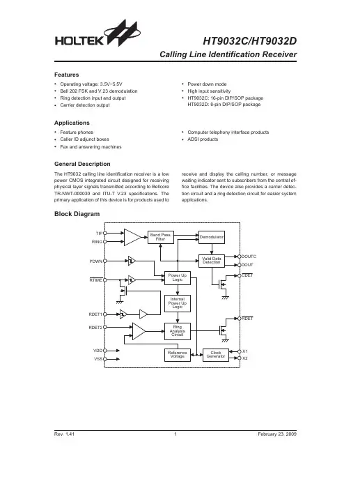
HT9032C/HT9032DCalling Line Identification ReceiverBlock DiagramRev.1.411February 23,2009Features·Operating voltage:3.5V~5.5V ·Bell 202FSK and V.23demodulation ·Ring detection input and output ·Carrier detection output·Power down mode ·High input sensitivity·HT9032C:16-pin DIP/SOP packageHT9032D:8-pin DIP/SOP packageApplications·Feature phones ·Caller ID adjunct boxes ·Fax and answering machines·Computer telephony interface products ·ADSI productsGeneral DescriptionThe HT9032calling line identification receiver is a low power CMOS integrated circuit designed for receiving physical layer signals transmitted according to Bellcore TR-NWT-000030and ITU-T V.23specifications.The primary application of this device is for products used toreceive and display the calling number,or message waiting indicator sent to subscribers from the central of-fice facilities.The device also provides a carrier detec-tion circuit and a ring detection circuit for easier systemapplications.Pin AssignmentPin DescriptionPin Name I/O Description Power InputsVDD¾Power-VDD is the input power for the internal logic.VSS¾Ground-VSS is ground connection for the internal logic.PDWN I A logic²1²on this pin puts the chip in power down mode.When a logic²0²is on this pin,the chip in power up mode.This is a Schmitt trigger input.ClockX1I A crystal or ceramic resonator should be connected to this pin and X2. This pin may be driven from an external clock source.X2O A crystal or ceramic resonator should be connected to this pin and X1. Ring DetectionsRDET1I It detects ring energy on the line through an attenuating network and enables the oscillator and ring detection.This is a Schmitt trigger input.RDET2I It couples the ring signal to the precision ring detector through an attenuating network. RDET=²0²if a valid ring signal is detected.This is a Schmitt trigger input.RTIME I/O An RC network may be connected to this pin in order to hold the pin voltage below2.2V be-tween the peaks of the ringing signal.This pin controls internal power up and activates the par-tial circuitry needed to determine whether the incoming ring is valid or not.The input is a Schmitt trigger input.The output cell structure is an NMOS output.FSK Signal InputsTIP I This input pin is connected to the tip side of the twisted pair wires.It is internally biased to1/2 V DD when the device is in power up mode.This pin must be DC isolated from the line.RING I This input pin is connected to the ring side of the twisted pair wires.It is internally biased to1/2 V DD when the device is in power up mode.This pin must be DC isolated from the line.Detection ResultsRDET O This open drain output goes low when a valid ringing signal is detected.When connected to PDWN pin,this pin can be used for auto power up.CDET O This open drain output goes low indicating that a valid carrier is present on the line.A hyster-esis is built-in to allow for a momentary drop out of the carrier.When connected to PDWN pin, this pin can be used for auto power up.DOUT O This pin presents the output of the demodulator when chip in power up mode.This data stream includes the alternate²1²and²0²pattern,the marking,and the data.At all other times,this pin is held high.DOUTC O This output presents the output of the demodulator when chip in power up mode and when an internal validation sequence has been successfully passed.This data stream does not include the alternate²1²and²0²pattern.This pin is always held high.TEST O Output pin for testing purposes only.NC¾No connectionRev.1.412February23,2009Absolute Maximum RatingsVoltages are referenced to V SS,except where noted.Supply Voltage.........................................-0.5V to6.0V All Input Voltages.................................................25mW Operating Temperature Range...................0°C to70°C Storage Temperature Range................-40°C to150°CNote:These are stress ratings only.Stresses exceeding the range specified under²Absolute Maximum Ratings²may cause substantial damage to the device.Functional operation of this device at other conditions beyond those listed in the specification is not implied and prolonged exposure to extreme conditions may affect device reliabil-ity.D.C.Characteristics Crystal=3.58MHz,Ta=0~70°CSymbol ParameterTest ConditionsMin.Typ.Max.Unit V DD ConditionsV DD Supply Voltage¾¾ 3.55 5.5V I DD1Supply Current5V PDWN=0(3.58MHz OSC on)¾ 3.25mAI DD2Supply Current5V PDWN=1and RTIME=0(3.58MHz OSC on and internalcircuits partially on)¾ 1.9 2.5mAI STBY Standby Current5V PDWN=1and RTIME=1(3.58MHz OSC off)¾¾1m A V IL Input Voltage Logic05V¾¾¾0.2V V DD V IH Input Voltage Logic15V¾0.8V¾¾V DD I OL Output Voltage Logic05V I OL=1.6mA¾¾0.1V V DD I OH Output Voltage Logic15V I OH=0.8mA0.9V¾¾V DD I IN Input Leakage Current,All Inputs5V¾-1¾1m AV T-Input Low Threshold Voltage5V RDET1,RTIME,PDWN 2.0 2.3 2.6VV T+Input High Threshold Voltage5V RDET1,RTIME,PDWN 2.5 2.75 3.0VV TRDET2Input Threshold Voltage5V RDET2 1.0 1.1 1.2VR IN Input DC Resistance5V TIP,RING¾500¾k WRev.1.413February23,2009A.C.Characteristics -FSK DetectionV SS =0V,Crystal=3.58MHz,Ta=0to 70°C,0dBm=0.7746Vrms @600W SymbolParameterTest ConditionsMin.Typ.Max.Unit V DD ConditionsInput Sensitivity:TIP,RING5V -40-45¾dBm S/NSignal to Noise Ratio 5V¾20¾dBBand Pass Filter 60Hz 550Hz 2700Hz 3300Hz5VFrequency ResponseRelative to 1700Hz @0dBm¾-64-4-3-34¾dBCarrier Detect Sensitivity5V ¾-48¾dBm t DOSC Oscillator Start Up Time5V ¾¾2¾ms t SUPD Power Up to FSK Signal Set Up Time 5V ¾15¾¾ms t DAQ Carrier Detect Acquisition Time 5V ¾¾14¾ms t DCHEnd of Data to Carrier Detect High5V¾8¾¾msRev.1.414February 23,2009Functional DescriptionThe HT9032is designed to be the physical layer de-modulator for products targeted for the caller ID market. The data signaling interface should conform to Bell202, which is described as follows:·Analog,phase coherent,frequency shift keying ·Logical1(Mark)=1200+/-12Hz·Logical0(Space)=2200+/-22Hz ·Transmission rate=1200bps·Data application=serial,binary,asynchronousThe interface should be arranged to allow simple data transmission from the terminating central office,to the CPE(Customer Premises Equipment),only when the CPE is in an on-hook state.The data will be transmitted in the silent period between the first and second power ring before a voice path is established.The transmission level from the terminating C.O.will be-13.5dBm+/-1.0. The worst case attenuation through the loop is expected to be-20dB.The receiver therefore,should have a sen-sitivity of approximately-34.5dBm to handle the worst case installations.The ITU-T V.23is also using the FSK signaling scheme to transmit data in the general switched telephone network.For mode2of the V.23,the modulation rate and characteristic frequencies are listed below:·Analog,phase coherent,frequency shift keying ·Logical1(Mark)=1300Hz ·Logical0(Space)=2100Hz·Transmission rate=1200bpsSince the band pass filter of the HT9032can pass the V.23signal,hence the HT9032also can demodulate the V.23signal.Ring detectionThe data will be transmitted in the silent period between the first and second power ring before a voice path is es-tablished.The HT9032should first detect a valid ring and then perform the FSK demodulation.The typical ring detection circuit of the HT9032is depicted below. The power ring signal is first rectified through a bridge circuit and then sent to a resistor network that attenu-ates the incoming power ring.The values of resistors and capacitor given in the figure have been chosen to provide a sufficient voltage at RDET1pin to turn on the Schmitt trigger input with approximately a40Vrms or greater power ring input from tip and ring.When V T+of the Schmitt is exceeded,the NMOS on the pin RTIME will be driven to saturation discharging capacitor on RTIME.This will initialize a partial power up,with only the portions of the part involved with the ring signal anal-ysis enabled,including RDET2pin.With RDET2pin en-abled,a portion of the power ring above1.2V is fed to the ring analysis circuit.Once the ring signal is qualified, the RDET pin will be sent low.Operation modeThere are three operation modes of the HT9032.They are power down mode,partial power up mode,and power up mode.The three modes are classified by the following conditions:Modes Conditions Current ConsumptionPower down PDWN=²1²and RTIME=²1²<1m APartial power up PDWN=²1²and RTIME=²0² 1.9mA typicallyPower up PDWN=²0² 3.2mA typicallyRev.1.415February23,2009Application CircuitsApplication circuit 1Application circuit 2Rev.1.416February 23,2009Normally,the PDWN pin and the RTIME pin control the operation mode of the HT9032.When both pins are HIGH,the HT9032is set at the power down mode,con-suming less than 1m A of supply current.When a valid power ring arrives,the RTIME pin will be driven below V T-and the portions of the part involved in the ring signal analysis are enabled.This is partial power up mode,consuming approximately 1.9mA typically.Once thePDWN pin is below V T-,the part will be fully powered up,and ready to receive FSK.During this mode,the device current will increase to approximately 3.2mA (typ).The state of the RTIME pin is now a ²don ¢t care ²as far as the part is concerned.After the FSK message has been re-ceived,the PDWN pin can be allowed to return to V DD and the part will return to the power down mode.Application circuit3¾power on resetApplication circuit4¾power on resetNote:reference C1=0.1m F R1=81k WRev.1.417February23,2009Package Information8-pin DIP(300mil)Outline DimensionsSymbolDimensions in milMin.Nom.Max.A355¾375B240¾260C125¾135D125¾145E16¾20F50¾70G¾100¾H295¾315I¾¾375Rev.1.418February23,200916-pin DIP (300mil)Outline Dimensions·MS-001d (see fig1)Symbol Dimensions in milMin.Nom.Max.A 780¾880B 240¾280C 115¾195D 115¾150E 14¾22F 45¾70G ¾100¾H 300¾325I¾¾430·MS-001d (see fig2)Symbol Dimensions in milMin.Nom.Max.A 735¾775B 240¾280C 115¾195D 115¾150E 14¾22F 45¾70G ¾100¾H 300¾325I¾¾430Rev.1.419February 23,2009Fig1.Full Lead PackagesFig2.1/2Lead Packages·MO-095a(see fig2)SymbolDimensions in milMin.Nom.Max.A745¾785B275¾295C120¾150D110¾150E14¾22F45¾60G¾100¾H300¾325I¾¾430Rev.1.4110February23,2009·MS-012SymbolDimensions in milMin.Nom.Max.A228¾244B150¾157C12¾20C¢188¾197D¾¾69E¾50¾F4¾10G16¾50H7¾10a0°¾8°Rev.1.4111February23,2009·MS-013SymbolDimensions in milMin.Nom.Max.A393¾419B256¾300C12¾20C¢398¾413D¾¾104E¾50¾F4¾12G16¾50H8¾13a0°¾8°Rev.1.4112February23,2009Product Tape and Reel SpecificationsReel DimensionsSOP8NSymbol Description Dimensions in mmA Reel Outer Diameter330.0±1.0B Reel Inner Diameter100.0±1.5C Spindle Hole Diameter13.0+0.5/-0.2D Key Slit Width 2.0±0.5T1Space Between Flange12.8+0.3/-0.2T2Reel Thickness18.2±0.2SOP16W(300mil)Symbol Description Dimensions in mmA Reel Outer Diameter330.0±1.0B Reel Inner Diameter100.0±1.5C Spindle Hole Diameter13.0+0.5/-0.2D Key Slit Width 2.0±0.5T1Space Between Flange16.8+0.3/-0.2T2Reel Thickness22.2±0.2Rev.1.4113February23,2009Carrier Tape DimensionsSOP8NSymbol Description Dimensions in mm W Carrier Tape Width12.0+0.3/-0.1P Cavity Pitch8.0±0.1E Perforation Position 1.75±0.1F Cavity to Perforation(Width Direction) 5.5±0.1D Perforation Diameter 1.55±0.1D1Cavity Hole Diameter 1.50+0.25/-0.00P0Perforation Pitch 4.0±0.1P1Cavity to Perforation(Length Direction) 2.0±0.1A0Cavity Length 6.4±0.1B0Cavity Width 5.2±0.1K0Cavity Depth 2.1±0.1t Carrier Tape Thickness0.30±0.05C Cover Tape Width9.3±0.1SOP16W(300mil)Symbol Description Dimensions in mm W Carrier Tape Width16.0±0.2P Cavity Pitch12.0±0.1E Perforation Position 1.75±0.10F Cavity to Perforation(Width Direction)7.5±0.1D Perforation Diameter 1.50+0.10/-0.00D1Cavity Hole Diameter 1.50+0.25/-0.00P0Perforation Pitch 4.0±0.1P1Cavity to Perforation(Length Direction) 2.0±0.1A0Cavity Length10.9±0.1B0Cavity Width10.8±0.1K0Cavity Depth 3.0±0.1t Carrier Tape Thickness0.30±0.05C Cover Tape Width13.3±0.1Rev.1.4114February23,2009Holtek Semiconductor Inc.(Headquarters)No.3,Creation Rd.II,Science Park,Hsinchu,TaiwanTel:886-3-563-1999Fax:886-3-563-1189Holtek Semiconductor Inc.(Taipei Sales Office)4F-2,No.3-2,YuanQu St.,Nankang Software Park,Taipei115,TaiwanTel:886-2-2655-7070Fax:886-2-2655-7373Fax:886-2-2655-7383(International sales hotline)Holtek Semiconductor Inc.(Shanghai Sales Office)G Room,3Floor,No.1Building,No.2016Yi-Shan Road,Minhang District,Shanghai,China201103Tel:86-21-5422-4590Fax:86-21-5422-4705Holtek Semiconductor Inc.(Shenzhen Sales Office)5F,Unit A,Productivity Building,Gaoxin M2nd,Middle Zone Of High-Tech Industrial Park,ShenZhen,China518057 Tel:86-755-8616-9908,86-755-8616-9308Fax:86-755-8616-9722Holtek Semiconductor Inc.(Beijing Sales Office)Suite1721,Jinyu Tower,A129West Xuan Wu Men Street,Xicheng District,Beijing,China100031Tel:86-10-6641-0030,86-10-6641-7751,86-10-6641-7752Fax:86-10-6641-0125Holtek Semiconductor Inc.(Chengdu Sales Office)709,Building3,Champagne Plaza,No.97Dongda Street,Chengdu,Sichuan,China610016Tel:86-28-6653-6590Fax:86-28-6653-6591Holtek Semiconductor(USA),Inc.(North America Sales Office)46729Fremont Blvd.,Fremont,CA94538,USATel:1-510-252-9880Fax:1-510-252-9885CopyrightÓ2009by HOLTEK SEMICONDUCTOR INC.The information appearing in this Data Sheet is believed to be accurate at the time of publication.However,Holtek as-sumes no responsibility arising from the use of the specifications described.The applications mentioned herein are used solely for the purpose of illustration and Holtek makes no warranty or representation that such applications will be suitable without further modification,nor recommends the use of its products for application that may present a risk to human life due to malfunction or otherwise.Holtek¢s products are not authorized for use as critical components in life support devices or systems.Holtek reserves the right to alter its products without prior notification.For the most up-to-date information, please visit our web site at .Rev.1.4115February23,2009。
MIC4832 Evaluation BoardLow Noise 220Vp-p EL DriverMLF and Micro LeadFrame are a registered trademark of Amkor Technology.General DescriptionThe MIC4832 is a low audible noise 220Vp-p electroluminescent lamp (EL) driver. Using advanced Bipolar, CMOS, DMOS (BCD) technology, the MIC4832 integrates a high voltage boost converter and an H-bridge driver for driving a large EL lamp. The MIC4832 can drive large panel displays for mobile phones, remote controls, MP3 players or automotive electronics where EL panels are used for backlighting.The MIC4832 offers design flexibility with adjustable lamp and boost converter frequencies, simply by applying external set resistors.Micrel’s new H-Bridge design reduces audible noise by creating smoother AC voltage across the EL panel. The smooth AC voltage waveform eliminates sudden changes in voltage, thus reducing the common cause of audible noise in EL drivers. RequirementsThe MIC4832 evaluation board requires an input power source that is able to deliver greater than 200mA at 1.8V.PrecautionsThe evaluation board does not have reverse polarity protection. Applying a negative voltage to the V IN terminal may damage the device.The MIC4832 evaluation board is tailored for a Li-Ion range input supply voltage. It should not exceed 5.5V on the input. The MIC4832 is a high voltage, low current device and should be handled with care to prevent a possible electrical buzz.Getting Started1. Connect an external supply to V IN . Applydesired input voltage to the V IN (J1) and ground terminal (J2) of the evaluation board, paying careful attention to polarity and supply voltage (1.8V ≤ V IN ≤ 5.5V). An ammeter may be placed between the input supply and the V IN terminal to the evaluation board. Ensure that the supply voltage is monitored at the V IN terminal. The ammeter and/or power lead resistance can reduce the voltage supplied to the input.2. Connect an EL panel . Connect the ELpanel to the VA (J4) and VB (J5) terminals. Note that polarity of the EL panel does not matter. 3. Enable/Disable the MIC4832 BoostRegulator . JP1 is the enable/disable jumper for the Boost Regulator portion of the MIC4832. Connecting JP1 to ground disables the boost regulator and connecting JP1 to V IN enables the boost regulator. A voltage signal may be applied to the center pin of JP1 to enable or disable the boost regulator. A low voltage signal (0V) will disable the boost regulator and a high voltage equal to V IN will enable the boost regulator. The enable voltage should rise and fall between high and low monotonically without interruptions. 4. Enable/Disable the MIC4832 H -Bridge .JP2 is the enable/disable jumper for the H-Bridge portion of the MIC4832. Connecting JP2 to ground disables the H-Bridge and connecting JP2 to V IN enables the H-Bridge. Disabling the H-Bridge does not disable the boost regulator. 5. Enable/Disable the EL panel . Both theBoost Regulator and the H-Bridge of the MIC4832 must be enabled in order for the EL panel to light up. For minimum shutdown current, both the Boost Regulator and the H-Bridge should be turned off. The EN jumper (JP3) connects the V IN to the inductor. This jumper may be used to enable or disable the EL panel on the evaluation board, without having to use JP1 and JP2 for evaluation purposes.Ordering InformationPart Number DescriptionMIC4832YMM EV 220Vpp MSOP Evaluation Board MIC4832YML EV 220Vpp MLF Evaluation BoardBoost Regulator Output VoltageThe boost regulator output voltage is set to 110V. The output peak-to-peak voltage across the EL panel is about 2 times the boost regulator output voltage (220Vp-p).EL Panel Size and Equivalent CircuitUsing laboratory data, it can be shown that the EL panel has an equivalent circuit equal to a series resistance (Rs) with a series capacitance (C) and a parallel resistance (Rp). For example, if an EL panel is 4in2, then the equivalent circuit is about 20nF of capacitance in series with 450Ω of resistance and 766kΩ of parallel resistance. Figure 1 and Table 1 shows close approximations of the equivalent circuit for different EL panel sizes.Figure 1. EL Panel Equivalent CircuitTable 1. EL Panel Equivalent Circuit Components Size (in2) 0.40 1.0 2.0 3.0 4.0 6.0 C(nF) 2 5 10 15 20 30 Rs (Ω) 4600 1800 900 600 450 300 Rp (MΩ) 7.66 3.05 1.53 1.02 0.7660.511Changing the Boost Regulator Frequency (f SW)The boost regulator switching frequency may be changed depending on the value of the R SW resistor. The R SW resistor on the evaluation board is equal to 332kΩ. The switching frequency may be calculated using the Rsw resistor by the following equation.()Ω=MR36(kHz)fSWSWLowering the switching frequency will deliver more power will be delivered to the EL panel by the boost regulator; however, the switching frequency of the boost regulator should not be low enough to create over-shoot at the SW pin or at the CS pin. Refer to Table 2 for recommended values.Changing the EL Lamp Frequency, f ELThe EL lamp frequency (H-Bridge frequency) may be changed depending on the value of the R EL resistor. The R EL resistor on the evaluation board is equal to 1.78MΩ. The EL lamp frequency may be calculated using the R EL resistor by the following equation.()()Ω=MR360HzfELELThe higher the EL lamp frequency, the brighter the EL panel; however, more brightness will require more input current, thus demand more input power. More power may be delivered to the EL lamp by increasing the input voltage or by lowering the switching frequency of the boost regulator. A table of recommended components for different EL panel sizes and EL lamp frequency is shown in Figure 2 and Table 2.Typical Application CircuitFigure 2. Typical Li-Ion Powered MIC4832 Circuit Table 2. Recommended R SW & R EL values for various panel sizesLamp Frequency(Hz) 100 200 300400 500 600 700 800 900Size (inch2) Capacitance(nF)Rel (MΩ) 2.82 1.69 1.1 0.8370.665 0.562 0.4710.4090.369Rsw (kΩ)240 252 273281 257 269 2810.4 2fsw (kHz) 150 143 132128 116 105 98Rsw (kΩ)257 295 3531 5fsw (kHz) 140 122 102Rsw (kΩ)300 3332 10fsw (kHz) 120 108Rsw (kΩ)3133 15fsw (kHz) 115Note: Table 2 applies to circuit shown in Figure 2.Figure 3. Evaluation Board SchematicBill of MaterialsNumber Manufacturer Description QtyItem PartC1 C1608X7R1A103K TDK 0.01µF Ceramic Capacitor, 10V, X7R, Size 0603 1C2 C1608X5R0J225K TDK 2.2µF Ceramic Capacitor, 6.3V, X5R, Size 0603 1C3 C2012C0G2E2272J TDK 0.0027µF Ceramic Capacitor, 250V, C0G, Size 0805 1L1 LPF2810BT-221M(B) ABCO 220µH, 110mA I SAT. 1 D1 BAS20-V-GS18 Vishay 200V/200mA Hi-Voltage Switching Diode 1R1 CRCW06033323FKEYE3 Vishay 332kΩ, 1%, 1/16W, Size 0603 1R2 CRCW06031784FKEYE3 Vishay 1.78MΩ, 1%, 1/16W, Size 0603 1R3, R4 CRCW06030R00FKEYE3 Vishay 0Ω, 1%, 1/16W, Size 0603 2U1 MIC4832 Micrel Low Noise 220Vp-p EL Driver 1Notes:1. TDK:2. ABCO:3. Vishay:4. Micrel, Inc.: Printed Circuit Board Layout (MSOP)MSOP TopMSOP BottomPrinted Circuit Board Layout (MLF®)MLF® TopMLF® Bottom。
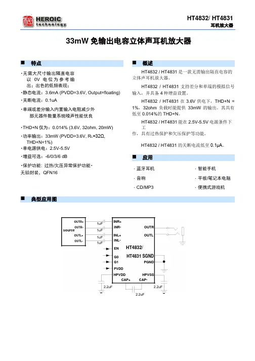
HT4832/ HT4831耳机放大器33mW免输出电容立体声耳机放大器⏹ 特点・无需大尺寸输出隔直电容以0V电位为参考输出;出色的低频表现;・静态电流:3.6mA (PVDD=3.6V, Output=floating) ・关断电流:0.1uA・单端或差分输入内置输入电阻减少外部元器件数量系统噪声性能优良・THD+N仅为:0.014% (3.6V, 32ohm, 20mW)・功率输出:33mW (PVDD=3.6V, R L=32Ω, THD+N=1%)・单电源供电:2.5V-5.5V・增益可选:-6/0/3/6 dB・保护功能:过热/欠压异常保护功能・无铅封装,QFN16 ⏹ 概述HT4832 / HT4831是一款无需输出隔直电容的立体声耳机放大器。
HT4832 / HT4831支持差分和单端的模拟信号输入,并具备4种增益设置。
HT4832 / HT4831在3.6V供电下,THD+N = 1%,32ohm负载时能提供33mW的输出。
其具有低至0.014%的THD+N。
HT4832 / HT4831能在2.5V-5.5V电源条件下工作,具有过热保护和欠压保护等功能。
HT4832 / HT4831的关断电流低至0.1μA。
⏹ 应用・蓝牙耳机・智能手机・音响・平板/笔记本电脑・CD/MP3・便携式游戏机⏹ 典型应用图OUTR+1uFINR+OUTR- INR- OUTR1uFSourceINL+ OUTLOUTL+ 1uFOUTL- INL-1uFHT4832/ENG0 HT4831 SGNDG1 PGNDPVDDHPVDD HPVSSCAP+ CAP-2.2uF 2.2uF2.2uF版权所有©2015,嘉兴禾润电子科技有限公司-1- 9/2015 – V1.0⏹ 引脚信息⏹ 引脚定义*1引脚号引脚I/O 功能HT4832 HT4831 名称1 1 INL- I 左声道反相输入端(差分-)2 2 INL+ I 左声道同相输入端(差分+)3 3 INR+ I 右声道同相输入端(差分+)4 4 INR- I 右声道反相输入端(差分-)5 7 OUTR O 右声道输出6 5 G0 I 增益设置7 6 G1 I 增益设置8 8 HPVSS P 电荷泵负电源9 10 CAP- P 电荷泵电容负端10 9 PGND P 地11 11 CAP+ P 电荷泵电容正端12 13 HPVDD P 电荷泵正电源13 16 EN I 芯片使能,低电平时芯片关断14 12 PVDD P 电源15 15 SGND I 信号地16 14 OUTL O 左声道输出注1 I: 输入端O: 输出端P: 电源/地⏹ 订购信息H T 4 8 3 X XX封装形式产品型号封装形式顶面标记工作温度范围包装和供货形式HT483XSQ QFN16 HT483X SQ -40℃~85℃UVWXYZ *2 (扩展工业级)注2:WXYZ/UVWXYZ 为内部生产跟踪随机编码。
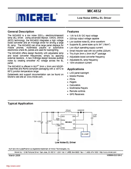
MIC4832Low Noise 220V PP EL DriverMLF and Micro LeadFrame is a registered trademark of Amkor Technologies, Inc.Micrel Inc. • 2180 Fortune Drive • San Jose, CA 95131 • USA • tel +1 (408) 944-0800 • fax + 1 (408) 474-1000 • General DescriptionThe MIC4832 is a low noise 220V PP electroluminescent lamp (EL) driver. Using advanced Bipolar, CMOS, DMOS (BCD) technology, the MIC4832 integrates a high voltage boost converter and an H-bridge driver for driving a large EL lamp. The MIC4832 can drive large panel displays for mobile phones, multimedia players or automotive electronics where EL panels are used for backlighting. The MIC4832 offers design flexibility with adjustable lamp and boost converter frequencies, simply by applying external resistors. A new H-Bridge design reduces audible noise by creating smoother AC voltage across the EL panel.The MIC4832 is offered in MLF ® 3mm x 3mm and MSOP-8 lead-free and RoHS-compliant packaging with a -40°C to 85°C junction temperature range.Datasheets and support documentation can be found on Micrel’s web site at: .Features• 1.8V to 5.5V DC input voltage • 220Vpp output voltage capable• Low audible noise EL drive waveform• Supports EL panel sizes up to 3in 2 (19cm 2) • Low 45µA operating supply current• Small inductor size with low profile (220uH) • Tiny 8-pin 3mm x 3mm MLF ® package • Adjustable boost converter frequency • Adjustable EL lamp frequency • 10nA shutdown currentApplications• LCD panel backlight • Mobile Phones • PDAs • Pagers • Calculators • Multimedia Players • Remote controls • GPS Receivers___________________________________________________________________________________________________________Typical ApplicationLow Noise EL DriverOrdering InformationPart Number Junction Temp. Range Package Lead FinishMIC4832YML –40° to +85°C 8-Pin 3mm × 3mm MLF®RoHS Compliant / Pb-Free / Halogen Free* MIC4832YMM –40° to +85°C 8-Pin MSOP RoHS Compliant / Pb-Free Note*MLF® is a GREEN RoHS-compliant package. Lead finish is NiPdAu. Mold compound is Halogen Free.Pin Configuration8-Pin MSOP (MM) 8-Pin 3mm × 3mm MLF® (ML)Pin DescriptionPin Number Pin Name Pin Function1 VDD Supply (Input): 1.8V to 5.5V for internal circuitry.Switch Resistor (External Component): Set switch frequency of the internal2 RSWpower MOSFET by connecting an external resistor to VDD. Connecting theexternal resistor to GND disables the switch oscillator and shuts down thedevice.EL Resistor (External Component): Set EL frequency of the internal H-bridge3 RELdriver by connecting an external resistor to VDD. Connecting the externalresistor to GND disables the EL oscillator.4 GND Ground5 SW Switch Node (Input): Internal high-voltage power MOSFET drain.Regulated Boost Output (External Component): Connect to the output capacitor6 CSof the boost regulator and connect to the cathode of the diode.7 VB EL Output: Connect to one end of the EL lamp. Polarity is not important.8 VA EL Output: Connect to one end of the EL lamp. Polarity is not important.Absolute Maximum Ratings(1)Supply Voltage (V DD)......................................–0.5V to 6.0V Output Voltage (V CS).....................................–0.5V to 120V EL Lamp Terminals (V A, V B)...................................V CS + 3V Switch Voltage (Vsw).....................................-0.5V to 120V Frequency Control Voltage(V RSW, V REL)...................................–0.5V to (V DD+0.3V) Storage Temperature (T S).........................–65°C to +150°C ESD Rating(4)..................................................................2kV Operating Ratings(2)Supply Voltage (V DD)....................................+1.8V to +5.5V Lamp Drive Frequency (f EL).......................60Hz to 1000Hz Switching Frequency (f SW).........................65kHz to 250kHz Ambient Temperature (T A)..........................–40°C to +85°C Package Thermal Resistance(3)MSOP(θJA).....................................................206°C/W MLF®(θJA).........................................................63°C/WElectrical Characteristics(5)V IN = V DD = 3.0V, R SW = 338KΩ, R EL = 1.78MΩ. T A = 25°C unless otherwise specified. Bold values indicate –40°C ≤ T A≤ +85°CParameter Condition MinTypMaxUnits On-resistance I SW = 100mA 3.8 7 OhmCS Voltage Variation 91 105 119Enable Input Low Voltage(turn-off)V DD = 1.8V to 5.5V 0.5 VEnable Input High Voltage (turn-on) V DD = 1.8V to 5.5V VDD-0.5VShutdown current R SW Resistor = LOW; R EL Resistor = LOW; V DD = 5.5V 0.01 0.5μA Input supply current R SW Resistor = HIGH;R EL Resistor = HIGH;V CS = 110V; V A, V B OPEN45 75 μAInput current including inductor V IN = V DD = 3.2V; R SW = 338KΩ, R EL = 1.78MΩ;L=220µH; R OUT =10kΩ; Lamp = 2in224 mAV A – V B output drive frequency R EL = 1.78MΩ158 200 242 HzSwitching transistor frequency R SW = 338KΩ90 112 134 kHzSwitching transistor dutycycle90 % Notes:1. Exceeding the absolute maximum rating may damage the device.2. The device is not guaranteed to function outside its operating rating.3. The maximum allowable power dissipation of any T A (ambient temperature) is P D(max) = (T J(max) – T A) / θJA. Exceeding the maximum allowablepower dissipation will result in excessive die temperature.4. Devices are ESD sensitive. Handling precautions recommended. Human body model, 1.5k in series with 100pF.5. Specification for packaged product only.Typical CharacteristicsFunctional DiagramFigure 1. MIC4832 Block DiagramFunctional DescriptionOverviewThe MIC4832 is a high-voltage EL driver with an AC output voltage of 220V peak-to-peak capable of driving EL lamps up to 3 in 2. Input supply current for the MIC4832 is typically 45µA reducing to 10nA in shutdown. The high voltage EL driver has two internal oscillators to control the switching MOSFET and the H-bridge driver. Both of the internal oscillators’ frequencies can be individually programmed through the external resistors to maximize the efficiency and the brightness of the EL lamp.RegulationReferring to Figure 1, initially power is applied to V DD . The internal feedback voltage is less than the reference voltage causing the internal comparator to go high which enables the switching MOSFET’s oscillator. When the switching MOSFET turns on, current flows through the inductor and flows into the switch. The switching MOSFET will typically turn on for 90% of the switching period. During the on-time, energy is stored in the inductor. When the switching MOSFET turns off, current flowing into the inductor forces the voltage across the inductor to reverse polarity. The voltage across the inductor rises until the external diode conducts and clamps the voltage at V OUT + V D1. The energy in the inductor is then discharged into the C OUT capacitor. The internal comparator continues to turn the switching MOSFET on and off until the internal feedback voltage is above the reference voltage. Once the internal feedback voltage is above the reference voltage, the internal comparator turns off the switching MOSFET’s oscillator.When the EL oscillator is enabled, V A and V B switch in opposite states to achieve a 220V peak-to-peak AC output signal. The external resistor that connects to the REL pin determines the EL frequency.V IN = 3.6V I IN = 17mA L = 220µH C OUT = 2.7nF LAMP = 2 in 2R SW = 300kR EL = 2.82MV A - V B (100V /d i v )V B (50V /d i v )V A (50V /d i v )Time (2ms/div)Figure 2. 100Hz Output Waveform Switching FrequencyThe switching frequency of the converter is controlled via an external resistor between R SW pin and V DD pin of the device. The switching frequency increases as the resistor value decreases. For resistor value selections, see the “Typical Characteristics: Switching Frequency vs. SW Resistor” or use the equation below. The switching frequency range is 65kHz to 250kHz, with an accuracy of ±20%. In general, the lower the switching frequency, the greater the input current is drawn to deliver more power to the output. However, the switching frequency should not be so low as to allow the voltage at the switch node or the CS pin to go beyond the absolute maximum voltage of those pins.()Ω=M R 36(kHz)f SW SWEL FrequencyThe EL lamp frequency is controlled via an external resistor connected between R EL pin and V DD pin of the device. The lamp frequency increases as the resistor value decreases. For resistor value selections, see the “Typical Characteristics: EL Frequency vs. EL Resistor” graph on page 4 or use the equation below. The EL lamp frequency range is 60Hz to 1000Hz, with an accuracy of ±20%.()()Ω=M R 360Hz f EL ELV IN = 3.6V I IN = 27mA L = 220µH C OUT = 2.7nF LAMP = 2 in 2R SW = 332kR EL = 1.78MV A - V B (100V /d i v )V B (50V /d i v )V A (50V /d i v )Time (2ms/div)Figure 3. 200Hz Output WaveformIn general, as the EL lamp frequency increases, the amount of current drawn from the battery will increase. The color of the EL lamp and the intensity are dependent upon its frequency.V IN = 3.6V I IN = 21mA L = 220µH C OUT = 2.7nF LAMP = 1 in 2R SW = 353kR EL = 1.1MV A - V B (100V /d i v )V B (50V /d i v )V A (50V /d i v )Time (2ms/div)Figure 4. 300Hz Output WaveformEnable FunctionThe MIC4832 is disabled by connecting the external resistor (Rsw) to GND. This turns off the switch oscillator of the boost converter. Connecting the external resistor (Rsw) to V DD enables the oscillator and turns on the device. The enable voltage should rise or fall monotonically without interruption.Application InformationInductorA 220µH Murata (LQH4C221K04) inductor is recommended for most applications. Generally, inductors with smaller values can handle more current. Lowering the inductance allows the boost regulator to draw more input current to deliver more energy every cycle. As a result, a lower value inductor may be used to drive larger panels or make the current panel brighter. However, caution is required as using a low value inductor with a low switching frequency may result in voltages exceeding the absolute maximum rating of the switch node and/or the CS pin. If the application uses a low input voltage (1.8 to 3V), a lower value inductor, such as 100µH, may be used in order to drive the EL lamp at max brightness without issue. DiodeThe diode must have a high reverse voltage (150V), since the output voltage at the CS pin can reach up to 130V. A fast switching diode with lower forward voltage and higher reverse voltage (150V), such as BAV20WS/BAS20W, can be used to enhance efficiency.Output CapacitorLow ESR capacitors should be used at the regulated boost output (CS pin) of the MIC4832 to minimize the switching output ripple voltage. The larger the output capacitance, the lower the output ripple at the CS pin. The reduced output ripple at the CS pin along with a low ESR capacitor improves the efficiency of the MIC4832 circuit. Selection of the capacitor value will depend upon the peak inductor current, inductor size, and the load. The MIC4832 is designed for use with an output capacitance as lowas 2.2nF. For minimum audible noise, the use of aC0G/NPO dielectric output capacitor is recommended. TDK and AVX offer C0G/NPO dielectric capacitors in capacitances up to 2.7nF at 200V to 250V rating in 0805 size. If output ripple is a concern a 0.01µF/200V X7R output capacitor is recommended.EL Lamp Terminals (VA, VB)An EL lamp is connected from VA to VB as the load. The high voltage alternated across VA and VB by the H-Bridge cycles generate luminance. The voltage at VA and VB should not exceed the voltageat V CS by more than 3V. This situation may become present when noisy enable signals such as those often generated by mechanical switches are appliedto the driver’s inputs. To prevent over voltage at VA and VB, 10kΩ resistors may be placed in series from VA to the EL panel and from VB to the EL panel. An alternative to the use of 10kΩ resistors is to apply a diode from the CS pin to VA and VB, where the cathode of the diode is on the CS side and the anode is on the VA and VB side, respectively.Application CircuitFigure 5: Typical Li-Ion Powered MIC4832 CircuitLamp Frequency(Hz) 100 200 300 400 500 600 700 800 900Size (inch2) Capacitance(nF)R EL (MΩ) 2.82 1.69 1.1 0.837 0.665 0.562 0.471 0.409 0.369R SW (kΩ)240 252 273 281 257 269 2810.4 2f SW (kHz) 150 143 132 128 116 105 98R SW (kΩ)257 295 3531 5f SW (kHz) 140 122 102R SW (kΩ)300 3332 10f SW (kHz) 120 108R SW (kΩ)3133 15f SW (kHz) 115Note: Table 1 applies to circuit shown in Figure 5.Table 1: Recommended R SW & R EL values for various panel sizesLayout RecommendationTopBottomPackage Information8-Pin MSOP (MM)8-Pin 3mm x 3mm MLF® (ML)分销商库存信息:MICRELMIC4832YML TR MIC4832YMM MIC4832YMM TR。

Jun. 2009 HT4863 Product Brief V2.0 2.2W 带立体声耳机输出模式的双声道音频功率放大器♦ 概述带立体声耳机输出模式的双声道音频功率放大器,用于多媒体监听器、电脑、便携式电视机、GPS、DPF(数码相框)、MP3/MP4/PMP、音响、DVD等通信和消费类电子产品;驱动4Ω~32Ω扬声器/耳机,系统简单、外围器件少,音质逼真,可媲美“国半”同类AB类音频功放产品,具有桥式和单端两种输出模式。
采用外部控制的低功耗关断模式,立体耳机放大模式,以及内部热敏关断保护机制,并利用电路的特性减小噪声(滴答声及爆裂声)和失真度,总谐波失真(THD+N)< 1.0%,封装形式有TSSOP-20/SOP-16/DIP-16。
HT4863MTE,接3Ω/4Ω负载2.5W (典型)/2.2W (典型);HT4863M/HT4863N,接8Ω负载1.2W(典型)。
♦ 电特性指标( 交流特性条件: 桥式输出模式、V DD = 5V, TA = 25℃,BTL mode:桥式模式、SE mode:单端模式 )HT4863Symbol Parameter ConditionsMin Typical Max Units (Limits)T A 工作温度范围﹣40+ 85 ℃V DD 电源电压范围 2.0 5.5 V V IN 输入电压范围-0.3 V DD +0.3 V I DD 静态工作电流VIN=0V, Io=0A ,HP-IN=0VIN=0V, Io=0A ,HP-IN=47 510mAI SD 静态关断电流 SHUTDOWN 接 GND 0.7 2 uA V IHV IL 耳机使能输入高电平 耳机使能输入低电平40.8 VV IH V IL 关断输入高电平 关断输入低电平1.4 0.4 V TWU启动时间1uF bypass cap(C6) 170 ms THD+N=1%, f=1kHz HT4863MTE,R L = 4Ω HT4863MTE,R L = 8Ω2.2 1.5W W Po 输出功率THD ≦10 %,f = 1kHz HT4863MTE,R L = 3Ω HT4863MTE,R L = 4Ω HT4863MTE,R L = 8Ω3.2 2.7 2W W W THD+N 总谐波失真+噪声 20Hz<f<1kHz R L = 4Ω,Po = 2 W R L = 8Ω,Po =1W 0.3 0.1% %PSRR 电源抑制比 VDD=5V,VRIPPLE=200mVRMS, RL=8Ω,CB=1.0uF67 dBX TALK 通道隔离度 f =1kHz ,CB =1.0uF , RL=8Ω 90 dB SNR信噪比 RL =8Ω,Po=1.1W98 dB♦典型应用图1 音频系统电路图♦管脚排布图2 、SOP16 和DIP 封装 图3 、TSSOP20 封装说明:HT4863M(SOP16 封装), HT4863N(DIP 封装),HT4863MT(TSSOP20 封装), HT4863MTE(TSSOP20 带散热片封装)♦封装外形信息图4 宽体TSSOP20 封装结构尺寸图图5 宽体SOP16 封装结构尺寸图图6 DIP16 封装结构尺寸图。
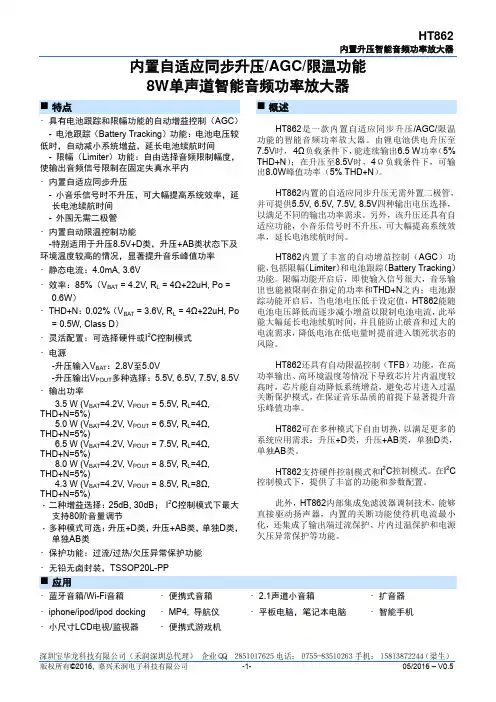
BK4832 对讲机射频功率放大器 1 概述BK4832 是一款单片集成的高增益、高效率 的射频功率放大器芯片。
关于HT4832,PAM8908,TPA6132耳放IC参数对比----万工Q1585749762欢迎咨询申请样品项目型号HT4832PAM8908TPA6132品牌禾润PAM TI工作电压 2.3--5.5V 2.3--5.5V 2.3--5.5V输出功率25mW/32Ω25mW/16Ω25mW/16Ω最小包装3000pcs3000pcs3000pcs 封装16-Pin,3mm×3mmThinQFN16-Pin,3mm×3mmThinQFN16-Pin,3mm×3mmThinQFN产品简介HT4832/HT4831是一款无需输出隔直电容的立体声耳机放大器。
HT4832/HT4831支持差分和单端的模拟信号输入,并具备4种增益设置。
HT4832/HT4831在3.6V供电下,THD+N=1%,32ohm负载时能提供33mW的输出。
其具有低至0.014%的THD+N。
HT4832/HT4831能在2.5V-5.5V电源条件下工作,具有过热保护和欠压保护等功能。
HT4832/HT4831的关断电流低至0.1μA。
T h e PA M8908s t e r e o he a d p h o n e d r i v e r i sdesigned for portableequipment where board spaceis at a premium.ThePAM8908uses a unique,patent pending architecture toproduce a ground-refer encedoutput from a single supply,e li m i n a t i n g t h e n e e d f o rl a r g e D C-b l o c k i n g c ap a c i t o r s,s a v i n g c o st,b o a r d s p a c e,a n dcomponent height.The PAM8908delivers up to25mW per channel into a16Ωload and has low0.03%THD+N.A high power-supplyrejection ratio allows thisdevice to operate from noisydigital supplies without anadditional linear regulator.The PAM8908operates from asingle supply from2.5V t o5.5V,h a s s h o r t-c i r c u it a n d o v e r temperatureprotection.Shutdown modereduces supply current to lessthan1uA.TPA6132A2(有时称作TPA6132)是DirectPath™立体声耳机放大器,无需使用外部直流阻隔输出电容器。
Technical SpecificationSchurter’s range of "Audio, DC and DIN Connectors" offers a cost effective solution for a wide range of applications.RangeThe range features 2.5mm, 3.5mm and 6.3mm Audio plugs and sockets.Low voltage DC plugs and sockets rated at 12V DC 0.5A for 5.5x2.1mm/5.5x2.5mm, 13.5V DC 2A for JSBP4 and 18V DC 2A for JSBP5.Miniature circular DIN plugs and sockets 3 to 8 pole.Plugs for all these ranges are rewirable and the sockets are fitted with solder or PCB tabs.Manufacturing Standards and Compatibility These cost effective connectors are designed and manufactured using dry assembly techniques. They comply with Japanese and Asian standards and are widely compatible to connectors fitted on consumer and industrial products, used worldwide.ApplicationsThese include connectors for low voltage power supplies, audio input and output, connections to controllers and transducer for game consoles, audio and video entertainment systems, musical instruments, amplifiers, transceiver’s, cleaning equipment, computer game cards, lap tops, printers, mobile / cordless phones, alarm systems, fitness machines.SpecificationThe specification shows operating characteristics.As with any connection products, to ensure customer satisfaction mating parts should be supplied from one source.For the combination chart please see Page 24.Technische SpezifikationSchurter’s Sortiment an “Audio, DC und DIN Stecker”bietet eine kostengünstige Alternative für ein weites Spektrum von Anwendungen.SortimentDas Sortiment umfasst 2.5mm, 3.5mm und 6.3mm Audio Stecker und Steckdosen.Niederspannungs DC Stecker und Steckdosen bis zu12V DC 0.5A für 5.5x2.1mm/5.5x2.5mm, 13.5V DC 2A für JSBP4 und 18V DC 2A für JSBP5.Miniatur DIN Stecker und Steckdosen von 3 bis 8 Pole.Stecker für alle Sortimente sind verkabelbar und die Steckdosen sind bestückt mit Löt oder PIN Anschlüssen.Herstellung und KompatibilitätDiese kostengünstigen Stecker sind entwickelt und hergestellt mit einer trockenen Montagetechnik (nicht Einspritz-Technik).Sie entsprechen Japanischen und Asiatischen Normen und sind kompatibel mit den meistenStecker/Steckdosen von Konsumer- und Industrie Produkten, weltweit.AnwendungenNiederspannungs Stromversorgung, Audio Ein- und Ausgänge, Verbindungen zu Regelgeräten und Wandlern/Verstärker für Spielgeräte, Audio- und Video Geräten, Musikinstrumente, Senderempfänger, Reinigungsgeräte, Computerspiele, Laptops, Drucker, Natels, Alarm Systeme und Fitnessgeräte.SpezifikationDie Spezifikation zeigt die Einsatz Charakteristik auf. Wie mit allen Steckverbindungen, für einen optimalen Wert, sollte man die Stecker und Steckdosen von der gleichen Quelle beziehen.Für die Kombinations Möglichkeiten konsultieren sie bitte Seite 24.T e c h n i c a l S p e c i f i c a t i o nT e c h n i s c h e S p e z i f i k a t i o n78.3Cable max.4.02.5Technical SpecificationSee Page 7 for complete technical specification and Page 24 for possible combinations.Technische Spezifikation Siehe Seite 7 für die vollständige technische Spezifikation undKombinationen.A u d i o C o n n e c t o r sA u d i o S t e c k e r9.5Cable max.4.02.5Cable max.4.012.019.51.0 1.482.5w w w.s c h u r t e r.c o m7.24.33.95.09.62.68.25.010.82.69.04.35.011.05.02.513.02.69.51.5Cable max.4.010.4Cable max.4.0 2.511.09.0Technical Specification See Page 7 for complete technical specification and Page 24 for possible combinations.Technische Spezifikation Siehe Seite 7 f ür die vollst ändige technischeSpezifikation und Seite 24 f ür m öKombinationen.A u d i o C o n n e c t o r s A u d i o S t e c k e r2.58.5 Cable max.3.0 Cable max.4.012.019.51.01.0102.52.5m m /3 P o l ew w w.s c h u r t e r.c o m2.63.06.58.02.62.74.010.04.02.62.85.02.35.010.4Cable max.4.0 1.59.011分销商库存信息: SCHURTER 4831.2220。
LM4832Digitally Controlled Tone and Volume Circuit with Stereo Audio Power Amplifier,Microphone Preamp Stage and National 3D SoundGeneral DescriptionThe LM4832is a monolithic integrated circuit that provides volume and tone (bass and treble)controls as well as a ste-reo audio power amplifier capable of producing 250mW (typ)into 8Ωor 90mW (typ)into 32Ωwith less than 1.0%THD.In addition,a two input microphone preamp stage,with volume control,capable of driving a 1k Ωload is imple-mented on chip.The LM4832also features National’s 3D Sound circuitry which can be externally adjusted via a simple RC network.For maximum system flexibility,the LM4832has an exter-nally controlled,low-power consumption shutdown mode,and an independent mute for power and microphone ampli-fiers .Boomer ®audio integrated circuits were designed specifically to provide high quality audio while requiring few external components.Since the LM4832incorporates tone and vol-ume controls,a stereo audio power amplifier and a micro-phone preamp stage,it is optimally suited to multimedia monitors and desktop computer applications.Key Specificationsn Output Power at 10%into:8Ω32Ω350mW(typ)100mW(typ)n THD +N at 75mW into32Ωat 1kHz 0.5%(max)n Microphone Input ReferredNoise 7µV(typ)n Supply Current 13mA(typ)n Shutdown Current4µA(max)Featuresn Independent Left and Right Output Volume Controls n Treble and Bass Control n National 3D Soundn I 2C Compatible Interfacen Two Microphone Inputs with Selector nSoftware Controlled Shutdown FunctionApplicationsn Multimedia Monitorsn Portable and Desktop ComputersBlock Diagram Connection DiagramBoomer ®is a registered trademark of National Semiconductor Corporation.DS100014-1FIGURE 1.LM4832Block DiagramDS100014-2Top ViewOrder Number LM4832N,LM4832M See NS Package Number N28B for DIP See NS Package Number M28B for SOICFebruary 1998LM4832Digitally Controlled Tone and Volume Circuit with Stereo Audio Power Amplifier,Microphone Preamp Stage and National 3D Sound©1998National Semiconductor Corporation Absolute Maximum Ratings(Note2)If Military/Aerospace specified devices are required, please contact the National Semiconductor Sales Office/ Distributors for availability and specifications.Supply Voltage 6.0V Storage Temperature−65˚C to+150˚C Input Voltage−0.3V to V DD+0.3V Power Dissipation(Note3)Internally limited ESD Susceptibility(Note4)2000V ESD Susceptibility(Note5)250V Junction Temperature150˚C Soldering InformationSmall Outline PackageVapor Phase(60sec.)215˚CInfrared(15sec.)220˚C See AN-450″Surface Mounting and their Effects on Product Reliability″for other methods of soldering surface mount devices.θJC(typ)—N28B21˚C/W θJA(typ)—N28B62˚C/W θJC(typ)—M28B15˚C/W θJA(typ)—M28B69˚C/WOperating RatingsTemperature RangeT MIN≤T A≤T MAX−40˚C≤T A≤85˚C Supply Voltage 4.5≤V DD≤5.5VElectrical Characteristics for Entire IC(Notes1,2)The following specifications apply for V DD=5V unless otherwise noted.Limits apply for T A=25˚C.Symbol Parameter ConditionsLM4832Units(Limits) Typical(Note6)Limit(Note7)V DD Supply Voltage V IN=0V,I O=0A 4.5V(min)5.5V(max)I DD Quiescent Power Supply Current1321mA(max) I SD Shutdown Current 2.59µA(max) INPUT ATTENUATORSA R Attenuator Range Attenuation at0dB SettingAttenuation at−14dB Setting1−15dB(max)dB(min)A S Step Size0dB to−14dB2dBGain Step Size Error0.1dB(max) E T Channel to Channel Tracking Error0.15dB(max) BASS CONTROLA R Bass Control Range f=100Hz,V IN=0.25V±12−14dB(min)14dB(max) A S Bass Step Size2dBE SE Bass Step Size Error0.5dB(max) E T Bass Tracking Error0.15dB(max) TREBLE CONTROLA R Treble Control Range f IN=10kHz,V IN=0.25V±12−13dB(min)13dB(max) A S Treble Step Size2dBE SE Treble Step Size Error0.1dB(max) E T Treble Tracking Error0.15dB(max) OUTPUT ATTENUATORSA R Attenuator Range Gain at+20dB SettingAttenuation at−40dB Setting+20dB to−40dB21dB(max)−42dB(min)A S Step Size2dBStep Size Error0.1dB(max) E T Channel to Channel Tracking Error0.1dB(max) AUDIO PATHV OS Output Offset Voltage V IN=0V350mV(max) 2Electrical Characteristics for Entire IC(Notes1,2)(Continued)The following specifications apply for V DD=5V unless otherwise noted.Limits apply for T A=25˚C.Symbol Parameter ConditionsLM4832Units(Limits) Typical(Note6)Limit(Note7)AUDIO PATHP O Output Power THD=1.0%(max),f=1kHz,Allcontrols at0dBR L=8Ω250mW(min)R L=32Ω9575mW(min) THD+N Total Harmonic Distortion+Noise All Controls at0dB,THD=10%,f=1kHzR L=8Ω350mWP O=200mW,R L=8Ω0.15%P O=75mW,R L=32Ω0.11%V O=1Vrms,R L=10Ω0.08% PSRR Power Supply Rejection Ratio C B=1µF,f=100Hz,V RIPPLE=100mVrms,All Controls at0dB Setting45dBA M Mute Attenuation f=1kHz,V IN=1V−75dBX TALK Cross Talk P O=200mW,R L=8Ω,All controls at0dB setting,f=1kHzLeft to Right−85dBRight to Left−72dB MICROPHONE PREAMP AND VOLUME CONTROLA V Preamp Gain0dB Gain0−1,1dB+20dB Gain2019,21dB+30dB Gain3029,31dBA R Attenuator Range Gain at+18dB Setting20dB(max)Attenuation at−42dB Setting−43dB(min) A S Step Size0dB to−42dB3dBStep Size Error0.4dB(max) V SWING Output Voltage Swing f=1kHz,THD<1.0%,R L=1kΩ 1.7V rmsE NO Input Referred Noise A-Weighted,Attenuator at0dB7µV(min) PSRR Power Supply Rejection Ratio f=100Hz,V RIPPLE=100mVrms,C B=1µF35dBA M Mute Attenuation−90dBX TALK Cross Talk Power Amp P O=200mW,f=1kHz−90dB THD+N Total Harmonic Distortion Plus Noise All controls at0dB,f=1kHz,V O=1V0dB Setting0.03%+20dB Gain0.03%+30dB Gain0.04%I2C BUS TIMINGf MAX Maximum Bus Frequency400kHzT START:HOLD Start Signal:Hold Time beforeClock/Data Transitions0.6µsT D;SETUP Data Setup Time0.1µsT C;HIGH Minimum High Clock Duration0.6µsT C;LOW Minimum Low Clock Duration 1.3µsT STOP;SETUP Stop Signal:Setup Time beforeClock/Data Transitions0.6µsI2C BUS INPUT AND OUTPUTV IL Input Low Voltage 1.5V(max)Electrical Characteristics for Entire IC(Notes1,2)(Continued)The following specifications apply for V DD=5V unless otherwise noted.Limits apply for T A=25˚C.Symbol Parameter ConditionsLM4832Units(Limits) Typical(Note6)Limit(Note7)I2C BUS INPUT AND OUTPUTV IH Input High Voltage3V(min) I IN Input Current0.15µAV O Output Voltage—SDA Acknowledge0.4V(max) V OL External Power Amp Disable Low0.4V(max) V OH External Power Amp Disable High4V(min) Note1:All voltages are measured with respect to the ground pins,unless otherwise specified.All specifications are tested using the typical applicationas shown in Figure1.Note2:Absolute Maximum Ratings indicate limits beyond which damage to the device may occur.Operating Ratings indicate conditions for which the device is func-tional,but do not guarantee specific performance limits.Electrical Characteristics state DC and AC electrical specifications under particular test conditions which guar-antee specific performance limits.This assumes that the device is within the Operating Ratings.Specifications are not guaranteed for parameters where no limit is given,however,the typical value is a good indication of device performance.Note3:The maximum power dissipation must be derated at elevated temperatures and is dictated by T JMAX,θJA,and the ambient temperature T A.The maximum allowable power dissipation is P DMAX=(T JMAX−T A)/θJA.For the LM4832,T JMAX=150˚C,and the typical junction-to-ambient thermal resistance,when board mounted,is69˚C/W assuming the M28B package.Note4:Human body model,100pF discharged through a1.5kΩresistor.Note5:Machine Model,220pF–240pF discharged through all pins.Note6:Typicals are measured at25˚C and represent the parametric norm.Note7:Limits are guaranteed that all parts are tested in production to meet the stated values.Typical Application CircuitDS100014-3FIGURE2.Typical Application Circuit4Pin DescriptionLEFT3D(1) RIGHT3D (28)An external RC network is connected across these pins.This function provides left-right channel cross coupling and cancellation to create an enhanced stereo channel separation effect.BYPASS(2)A0.1µF capacitor is placed betweenthis pin and ground to provide an ACground for the internal half-supplyvoltage reference.The capacitor at thispin affects“click-pop”and THDperformance.Turn-on and turn-off timesare also determined by this capacitor.Refer to the Application Informationsection for more information.POWER AMP OUT LEFT(3) RIGHT(26)These outputs are intended to drive8Ωspeakers or32Ωheadphones.These outputs should be AC-coupled to the loads.Refer to the Application Information section for more information.POWER GND(4)This pin provides the high current return for the power output stage MOSFETs and digital circuitry.LOOP OUT (8,21) LOOP IN(5, 24)These pins allow an external signal processor access to the stereo signal. Please see the Application Information section for more information.TONE OUT (6,23)These pins are connected to the tone control op amp outputs and drive the power amplifier inputs.Refer to the Application Information section for more information.TONE IN (7,22)These pins are connected to the inputs of the tone control op amps.A capacitor between the Tone In and Tone Out pins sets the frequency response of the tone functions.Please refer to the Application Information section for more information.INPUTS (9,20)These pins are the stereo inputs for the LM4832.These pins should beAC-coupled to the input signals.ANALOG GND(10)This pin is the AC analog ground for the line level AC signal inputs.MIC INPUTS (11,12)These pins are the two independent selectable microphone inputs.These pins should be AC-coupled.MIC OUT (14)This pin is the output for the microphone amplifier and should be AC-coupled to the load.V DD (13,25)These pins are for the5V supply.These pins should be separately bypassed by 0.1µF,or higher,film capacitors.The5V supply should be bypassed by a10µF, or higher,tantalum or aluminum electrolytic capacitor.ADDRESS BITS(15, 16)These pins are used to determine theI2C address for the LM4832.CLOCK(17)This pin is the input for the I2C clocksignal.DATA(18)This pin is the input for the I2C datasignal.GENERALPURPOSEOUTPUT(19)This pin provides a general purposeTTL/CMOS output.Please refer to theApplication Information section for moreinformation.RESET(27)This pin is a TTL/CMOS input which isused to reset the chip logic and states.Typical Performance CharacteristicsTHD+N vsFrequency,8ΩDS100014-4THD+N vsFrequency,32ΩDS100014-5THD+N vsFrequency,1k ΩDS100014-6THD+N vs Output Power DS100014-7THD+N vs Output Power DS100014-8THD+N vs Output PowerDS100014-9Power Amplifier Crosstalk DS100014-10Power Amplifier Noise Floor DS100014-11Power Amplifier Attenuation vs FrequencyDS100014-12 6Typical Performance Characteristics(Continued)Power SupplyRejection RatioDS100014-13Power Dissipationvs Output PowerDS100014-14Power DeratingCurveDS100014-15Mic Amplifer Crosstalkfrom Power AmplifierDS100014-16Mic AmplifierNoise FloorDS100014-17Mic Amplifier Attenuationvs FrequencyDS100014-18Mic Amplifier Gainvs FrequencyDS100014-19Mic Amplifier THD+Nvs FrequencyDS100014-20Loop-out THD+Nvs FrequencyDS100014-21Typical Performance Characteristics(Continued)Timing DiagramBass Response vs FrequencyDS100014-22Treble Response vs FrequencyDS100014-23Bass and Treble Response vs FrequencyDS100014-24Supply Current vs TemperatureDS100014-25DS100014-26FIGURE 3.I 2C Bus Format 8Timing Diagram(Continued)DS100014-27See Electrical Characteristics section fortiming specificationsFIGURE4.I2C Timing DiagramTruth TablesSOFTWARE SPECIFICATIONChip AddressMSB LSB10000*E.C.*E.C.0*E.C.=Externally ConfiguarableData Bytes(Brief Description)MSB LSB Function000X X D2D1D0Input Volume Control 001X D3D2D1D0Bass Control010X D3D2D1D0Treble Control011D4D3D2D1D0Right Output Vol./Mute 100D4D3D2D1D0Left Output Vol./Mute 101X D11D10D01D00Mic Input and Gain 110D4D3D2D1D0Microphone Volume 111D40D30D20D10D00General ControlInput Volume ControlMSB LSB Attenuation(dB)000X X0000000X X001−2000X X010−4000X X011−6000X X100−8000X X101−10000X X110−12000X X111−14Input Volume Control Power Up State X X000Input Volume Controlat0dB AttenuationBass ControlMSB LSB Level(dB)001X0000−12001X0001−10001X0010−8001X0011−6001X0100−4001X0101−2001X01100001X01112001X10004001X10016001X10108001X101110001X110012Bass ControlPower Up StateX0110Bass Control is Flat 10Truth Tables(Continued)Treble ControlMSB LSB Level(dB)010X0000−12010X0001−10010X0010−8010X0011−6010X0100−4010X0101−2010X01100010X01112010X10004010X10016010X10108010X101110010X110012X0110Treble Control is FlatTreble ControlPower Up StateLeft Volume ControlMSB LSB Function10000000201000000118 100..................10011101−3810011110−4010011111Left Channel Mute11111Left Channel is MutedLeft Volume ControlPower Up StateGeneral ControlMSB LSB Function1110Chip On1111Chip Shutdown1110G.P.O.Output Low1111G.P.O.Output High1110Stereo Enhance Off1111Stereo Enhance On1110Stereo Operation1111Mono Force On1110External Loop Disable1111External Loop EnableGeneral Control00000Power Up StateTruth Tables(Continued)Right Volume ControlMSB LSB Level(dB) 01100000200110000118 011..................01111100−3801111110−4001111111Right Channel Mute Right Volume ControlPower Up State11111Right Channel Is Muted Microphone Input Selection and GainMSB LSB Function101X00Mic Input1101X01Mic Input2101X1X Mic Input1and2101X00Mic Gain(+0dB)101X01Mic Gain(+20dB)101X10Mic Gain(+30dB)Mic Input Sel.and Gain Power Up State X1000Mic1is selectedwith a+30dB gainMicrophone Volume ControlMSB LSB Function11000000181100000115110..................11010100−4211010101Microphone Muted Mic Volume ControlPower Up State10101Microphone Muted 12Application InformationGROUNDINGIn order to achieve the best possible performance,certain grounding techniques should be followed.All input reference grounds should be tied with their respective source grounds and brought back to the power supply ground separately from the output load ground returns.These input grounds should also be tied in with the half-supply bypass ground. Bringing the ground returns for the output loads back to the supply separately will keep large signal currents from inter-fering with the stable AC input ground references. LAYOUTAs stated in the Grounding section,placement of ground re-turn lines is critical for maintaining the highest level of sys-tem performance.It is not only important to route the correct ground return lines together,but also important to be aware of where those ground return lines are routed in conjunction with each other.The output load ground returns should be physically located as far as reasonably possible from low signal level lines and their ground return lines.Critical signal lines are those relating to the microphone amplifier section, since these lines generally work at very low signal levels. SUPPLY BYPASSINGAs with all op amps and power op amps,the LM4832re-quires the supplies to be bypassed to avoid oscillation.To avoid high frequency instabilities,a0.1µF metallized-film or ceramic capacitor should be used to bypass the supplies as close to the chip as possible.For low frequency consider-ations,a10µF or greater tantalum or electrolytic capacitor should be paralleled with the high frequency bypass capaci-tor.If power supply bypass capacitors are not sufficiently large, the current in the power supply leads,which is a rectified ver-sion of the output current,may be fed back into internal cir-cuitry.This internal feedback signal can cause high fre-quency distortion and oscillation.If power supply lines to the chip are long,larger bypass ca-pacitors could be required.Long power supply leads have in-ductance and resistance associated with them,that could prevent peak low frequency current demands from being met.The extra bypass capacitance will reduce the peak cur-rent requirements from the power supply lines.POWER-UP STATUSOn power-up or after a hard reset,the LM4832registers will be initialized with the default values listed in the truth tables. By default,the LM4832power and microphone outputs are muted,the tone controls are all flat,National3D Enhance is off,the chip is in stereo mode,and the microphone input1is selected with+30dB of gain.CLICK AND POP CIRCUITRYThe LM4832contains circuitry to minimize turn-on transients or“click and pops”.In this case,turn-on refers to either power supply turn-on or the device coming out of shutdown mode.When the deviceis turning on,the amplifiers are inter-nally configured as unity gain buffers.An internal current source charges the bypass capacitor on the bypass pin. Both the inputs and outputs ideally track the voltage at the bypass pin.The device will remain in buffer mode until thebypass pin has reached its half supply voltage,1/2VDD.As soon as the bypass node is stable,the device will becomefully operational.Although the bypass pin current source cannot be modified,the size of the bypass capacitor,C B,can be changed to alterthe device turn-on time and the amount of“click and pop”.Byincreasing C B,the amount of turn-on pop can be reduced.However,the trade-off for using a larger bypass capacitor isan increase in the turn-on time for the device.Reducing C Bwill decrease turn-on time and increase“click and pop”.If C Bis too small,the LM4832can develop a low-frequency oscil-lation(“motorboat”)when used at high gains.There is a linear relationship between the size of C B and theturn-on time.Some typical turn-on times for different valuesof C B are:C b T ON0.01µF20ms0.1µF200ms0.22µF420msIn order to eliminate“click and pop”,all capacitors must bedischarged before turn-on.Rapid on/off switching of the de-vice or shutdown function may cause the“click and pop”cir-cuitry to not operate fully,resulting in increased“click andpop”noise.The output coupling cap,C O,is of particular con-cern.This capacitor discharges through an internal20kΩre-sistor.Depending on the size of C O,the time constant can bequite large.To reduce transients,an external1kΩ–5kΩre-sistor can be placed in parallel with the internal20kΩresis-tor.The tradeoff for using this resistor is an increase in quies-cent current.COUPLING CAPACITORSBecause the LM4832is a single supply circuit,all audio sig-nals must be capacitor coupled to the chip to remove the2.5V DC bias.All audio inputs have20kΩinput impedances,so the AC-coupling capacitor will create a high-pass filterwithf−3dB=1/(2π*20kΩ*C IN).The amplifier outputs also need to be AC-coupled to theloads.The high-pass filter is comprised of the output loadand the coupling capacitor,where the filter cutoff is atf−3dB=1/(2π*R LOAD*C OUT).POWER AMPLIFIERThe power amplifiers in the LM4832are designed to drive8Ωor32Ωloads at200mW(continuous)and75mW(con-tinuous),respectively,with1%THD+N.As shown in the Typi-cal Performance Characteristics,the power amplifiers typi-cally drive4Ωloads at350mW,but with a slight increase inhigh-frequency THD.As discussed above,these outputsshould be AC-coupled to the output load.MICROPHONE AMPLIFIERThe microphone preamplifier is intended to amplify low-levelsignals for signal conditioning.The microphone inputs canbe directly connected to microphone networks.The micro-phone amplifier has enough output capability to drive a1kΩload.All microphone inputs and outputs must be AC-coupled.Application Information(Continued)I2C INTERFACEThe LM4832uses a serial bus,which conforms to the I2C protocol,to control the chip’s functions with two wires:clock and data.The clock line is uni-directional.The data line is bi-directional(open-collector)with a pullup resistor(typically 10kΩ).The maximum clock frequency specified by the I2C standard is400kHz.In this discussion,the master is the controlling microcontroller and the slave is the LM4832. The I2C address for the LM4832is determined using the Ad-dress Bit1and Address Bit2TTL/CMOS inputs on the chip. The LM4832’s four possible I2C chip addresses are of the form10000X2X10(binary),where the X2and X1bits are de-termined by the voltage levels at the Address Bit2and Ad-dress Bit1pins,respectively.If the I2C interface is used to address a number of chips in a system and the LM4832’s chip address can be changed to avoid address conflicts. The timing diagram for the I2C is shown in Figure2.The data is latched in on the stable high level of the clock and the data line should be held high when not in use.The timing diagram is broken up into six major sections:The“start”signal is generated by lowering the data signal while the clock signal is high.The start signal will alert all de-vices attached to the I2C bus to check the incoming address against their own chip address.The8-bit chip address is sent next,most significant bit first. Each address bit must be stable while the clock level is high. After the last bit of the address is sent,the master checks for the LM4832’s acknowledge.The master releases the data line high(through a pullup resistor).Then the master sends a clock pulse.If the LM4832has received the address cor-rectly,then it holds the data line low during the clock pulse. If the data line is not low,then the master should send a “stop”signal(discussed later)and abort the transfer.The8bits of data are sent next,most significant bit first. Each data bit should be valid while the clock level is stable high.After the data byte is sent,the master must generate another acknowledge to see if the LM4832received the data.If the master has more data bytes to send to the LM4832, then the master can repeat the previous two steps until all data bytes have been sent.The“stop”signal ends the transfer.To signal“stop”,the data signal goes high while the clock signal is high.3D AUDIO ENHANCEMENTThe LM4832has a3D audio enhancement effect that helps improve the apparent stereo channel separation when,be-cause of cabinet or equipment limitations,the left and right speakers are closer to each other than optimal.An external RC network,shown in Figure3,is required to en-able the effect.The amount of the effect is set by the20kΩresistor.A0.1µF capacitor is used to reduce the effect at fre-quencies below80Hz.Decreasing the resistor size will make the3D effect more pronounced and decreasing the ca-pacitor size will raise the cutoff frequency for the effect. The680kΩresistor across the0.1µF capacitor reduces switching noise by discharging the capacitor when the effect is not in use.TONE CONTROL RESPONSEBass and treble tone controls are included in the LM4832. The tone controls use two external capacitors for each ste-reo channel.Each has a corner frequency determined by the value of C2and C3(see Figure4)and internal resistors in the feedback loop of the internal tone amplifier. Typically,C2=C3and for100Hz and10kHz corner fre-quencies,C2=C3=0.0082µF.Altering the ratio between C2and C3,changes the midrange gain.For example,if C2 =2(C3),then the frequency response will be flat at20Hz and20kHz,but will have a6dB peak at1kHz.With C=C2=C3,the treble turn-over frequency is nominallyf TT=1/(2πC(14kΩ))and the bass turn-over frequency is nominallyf BT=1/(2πC(30.4kΩ)),when maximum boost is chosen.The inflection points(the frequencies where the boost or cut is within3dB of the final value)are,for treble and bass respectively,f TI=1/(2πC(1.9kΩ))f BI=1/(2πC(169.6kΩ))Increasing the values of C2and C3decreases the turnover and inflection frequencies:i.e.,the Tone Control Response Curves shown in Typical Performance Section will shift left when C2and C3are increased and shift right when C2and C3are decreased.With C2=C3=0.0082µF,2dB steps are achieved at100Hz and10kHz.Changing C2and C3to 0.01µF shifts the2dB step frequency to72Hz and8.3 kHz.If the tone control capacitors’size is decreased these frequencies will increase.With C2=C3=0.0068µF the2dB steps take place at130Hz and11.2kHz.DS100014-28FIGURE5.3D Effect Components14Application Information(Continued)GENERAL PURPOSE OUTPUT PINThe General Purpose Output pin is intended to be used as a control signal for other devices,such as an external power amplifier.This pin is controlled through the I 2C interface and is not relatedto any other functions within the LM4832.Refer to the Truth Tables section for the proper I 2C data bits to uti-lize this function.Figure 7shows an example of using the General Purpose Output to interface with an external power amp.In this case,the external power amp is the LM4755stereo 10watt perchannel (rms)power amplifier with mute.AC-coupling ca-pacitors must be used to remove the DC bias present be-tween the LM4832outputs and the external power amplifier inputs.Prior to placing any of the preamp circuitry in shutdown,the General Purpose Output should be used to disable the exter-nal power amplifier.This will prevent any shutdown transients in the preamp circuitry from being amplified by the external power amplifier.LOOP IN/OUT PINSThe Loop In and Loop Out pins are used when an application requires a special function to be performed on the audio sig-nal.As shown in Figure 7,the audio signal is taken from the Loop Out pin and sent to an external signal processor.After the signal is processed externally,it is fed back into the Loop In pin.An example of where this functionality would be used is com-puter speakers.The external loop could be used to provide bass boost to counteract the speaker’s natural or baffle-induced rolloff.Since the Loop In pin goes directly to the input of a CMOS amplifier,the input impedance is very high.The Loop Out pin is driven by the input attenuation amplifier,which is capable of driving impedances as low as 1k Ω.DS100014-29FIGURE 6.Tone Control DiagramDS100014-3010W/ch System with I 2C Controlled Tone,Volume and 3D SoundApplication Information(Continued)LM4832SAMPLE LAYOUTLAYOUT PARTS LISTName Type QuantityCapacitors:C OUT1000µF,elec.,Digikey#P62054 C MOUT47µF,elec.,Digikey#P52021 C S0.33µF,film,Digikey#P46693 C TONE8200pF,ceramic,Digikey#P48234 C LIN,C MIN,C IN1µF,film,Digikey#E11056 C B0.33µF,film,Digikey#EF13341 C10.1µF,film,Digikey#EF11041 Resistors(all resistors:Digikey#(Value)QBK):R120kΩ,1/4W1 R2680kΩ,1/4W1 R DATA1kΩ,1/4W1 R GND100Ω,1/4W1 R PD100kΩ,1/4W1LAYOUT PARTS LISTName Type QuantityConnectors:Banana JackBlack Mouser#164-62183 Red Mouser#164-62183 RCA Jack Mouser#16PJ0977 StereoHeadphoneShogyo#JJ-0357-3RT1 Mono Miniplug Shogyo#JJ-0357-B2 36-pinCentronicsDigikey#1036RF1 LAYOUT DESCRIPTIONThe layout given in the following pages is meant to be con-nected to a PC by a parallel port(printer)cable.The board is controlled by software for a Windows PC.The parallel cable must be the standard type used for hooking up a printer to a PC:one end is a DB-25connector andthe other is a36pin Centronics connector.Banana connections are provided for V DD,ground,and am-plifier outputs.Amplifier outputs are also routed to a stereo headphone jack.RCA connections are provided for amplifier inputs,loop in,loop out,and microphone out.Mono mini-plug connectors are provided for microphone inputs.If required,microphones can be biased using the resistors R MIC1and R MIC2.This layout is set up to allow the use of the internal tone-control circuitry or the external loop.The jumper next to each C LIN capacitor controls which route the signal should take.DS100014-3116。
.HT4832/ HT4831耳机放大器33mW免输出电容立体声耳机放大器特点・无需大尺寸输出隔直电容以0V电位为参考输出;出色的低频表现;・静态电流:3.6mA (PVDD=3.6V,Output=floating)・关断电流:0.1uA・单端或差分输入内置输入电阻减少外部元器件数量系统噪声性能优良・THD+N仅为:0.014% (3.6V, 32ohm, 20mW) ・功率输出:33mW (PVDD=3.6V, R L=32Ω, THD+N=1%)・单电源供电:2.5V-5.5V・增益可选:-6/0/3/6 dB・保护功能: 过热/欠压异常保护功能・无铅封装,QFN16概述HT4832 / HT4831是一款无需输出隔直电容的立体声耳机放大器。
HT4832 / HT4831支持差分和单端的模拟信号输入,并具备4种增益设置。
HT4832 / HT4831在3.6V供电下,THD+N = 1%,32ohm负载时能提供33mW的输出。
其具有低至0.014%的THD+N。
HT4832 / HT4831能在2.5V-5.5V电源条件下工作,具有过热保护和欠压保护等功能。
HT4832 / HT4831的关断电流低至0.1μA。
应用・蓝牙耳机・智能手机・音响・平板/笔记本电脑・CD/MP3・便携式游戏机典型应用图OUTR+ 1uF INR+OUTR- INR- OUTR1uFSourceINL+ OUTLOUTL+ 1uFOUTL- INL-1uFHT4832/ENG0HT4831 SGNDG1 PGNDPVDDHPVDD HPVSSCAP+ CAP-2.2uF 2.2uF2.2uF9/2015 –版权所有©2015, 嘉兴禾润电子科技有限公司-1-V1.0HT4832/ HT4831耳机放大器引脚信息引脚定义*1引脚号引脚I/O 功能HT4832 HT4831 名称1 1 INL- I 左声道反相输入端(差分-)2 2 INL+ I 左声道同相输入端(差分+)3 3 INR+ I 右声道同相输入端(差分+)4 4 INR- I 右声道反相输入端(差分-)5 7 OUTR O 右声道输出6 5 G0 I 增益设置7 6 G1 I 增益设置8 8 HPVSS P 电荷泵负电源9 10 CAP- P 电荷泵电容负端10 9 PGND P 地11 11 CAP+ P 电荷泵电容正端12 13 HPVDD P 电荷泵正电源13 16 EN I 芯片使能,低电平时芯片关断14 12 PVDD P 电源15 15 SGND I 信号地16 14 OUTL O 左声道输出注1 I: 输入端O: 输出端P: 电源/地9/2015 –版权所有©2015, 嘉兴禾润电子科技有限公司-2-V1.0HT4832/ HT4831耳机放大器订购信息H T 4 8 3 X XX封装形式产品型号封装形式顶面标记工作温度范围包装和供货形式HT483XSQ QFN16 HT483X SQ -40℃~85℃UVWXYZ *2 (扩展工业级)注2:WXYZ/UVWXYZ 为内部生产跟踪随机编码。
CS4863双2.2W音频放大和立体声耳机功能产品说明书第 1 页共 21 页1、概 述CS4863是双桥接的音频功率放大器。
当电源电压为5V时,在保证总谐波失真、噪声失真之和小于1.0%的情况下,可向4Ω负载提供2.2W的输出功率或者可向3Ω负载提供2.5W的输出功率。
另外,当驱动立体声耳机时,耳机输入端允许放大器工作在单端模式。
该系列音频功率放大器为表面贴装电路,极少的外围元器件,高品质的输出功率。
对于简单的音频系统设计,CS4863片内集成了双桥扬声器放大和立体声耳机放大。
CS4863电路的特点为外部控制,低功耗关断模式,立体声耳机放大模式,和内部过热保护,并且在电路中减少了“开机浪涌脉冲”。
CS4863主要应用于多媒体监视器、便携式和台式电脑、便携式电视。
主要特点如下:●立体声耳机放大模式●“开机浪涌脉冲”抑制电路●单位增益稳定●过热保护电路●封装形式:DIP16 / SOP16 / TSSOP20关键参数:●P O为1% THD+N●CS4863LQ 负载为3Ω,4Ω典型为2.5W,2.2W●CS4863MTE负载为3Ω,4Ω典型为2.5W,2.2W●CS4863MTE负载为8Ω典型为 1.1W●CS4863 负载为8Ω典型为 1.1W●单端模式(在75mW、32Ω时)THD+N 0.5%(最大)●关断电流典型为0.7µA●工作电压范围 2.0V~5.5V2、引脚排列图SOP16 (DIP16) TSSOP20第 2 页共 21 页第 3 页共 21 页3、电特性3.1、 极限参数除非另有规定,T amb =25℃参 数 名 称额 定 值 单 位 电源电压 6.0 V 输入电压 -0.3~V DD +0.3 V 存储温度 -65~+150 ℃ 功耗内部限制 ESD 电压(人体模式) 2000 V ESD 电压(机器模式) 200V V 结温 150 ℃ 工作温度-40~+85℃ DIP 封装 245 ℃ 焊接温度(10秒)SOP 封装250℃ θJC -M16B 20 ℃/W θJA - M16B 80℃/W ℃/W θJC - M16A20℃/W ℃/W θJA - M16A63℃/W ℃/W θJC -MTC20 20℃/W ℃/W θJA -MTC20 80℃/W ℃/W 热阻θJC -MXA20A 2℃/W℃/W3.2、电气参数电气参数(整个电路)(V DD =5V,T A =25℃) CS4863 符号 参数条件典型极限单位 (极限)2 V(min) V DD电源电压5.5 V(max) I DD 静态功率电源电流 V IN =0V ,I O =0A ,HP-IN=0VV IN =0V ,I O =0A ,HP-IN=4V 11.5 5.820 6mA(max)mA(min)mAI SD 关断电流 V DD 与SHUTDOWN 脚相连0.7 2 µA(min)V IH 耳机高电平输入电压 4 V(min)V IL 耳机低电平输入电压0.8 V(max)GSW深圳市国顺威电子有限公司第 4 页共 21 页电气参数(电路工作在桥接模式)(V DD =5V,T A =25℃)CS4863 符号参数条件典型极限 单位 (极限)V OS输出偏移电压 V IN =0V 5 50 mV(max)P O输出功率THD+N=1%,f=1kHz CS4863MTE , R L =3Ω CS4863LQ , R L =3Ω CS4863MTE , R L =4Ω CS4863LQ , R L =4Ω CS4863, R L =8ΩTHD+N=10%,f=1kHz CS4863MTE ,R L =3Ω CS4863LQ , R L =3Ω CS4863MTE ,R L =4Ω CS4863LQ , R L =4Ω CS4863, R L =8Ω THD+N=1%,f=1kHz ,R L =32Ω 2.5 2.5 2.2 2.2 1.1 3.2 3.2 2.7 2.7 1.5 0.341.0W W W W W(min) W W W W W W THD+N总谐波失真和噪声20Hz ≤f ≤20KHz ,A VD =2CS4863MTE ,R L =4Ω,P O =2W CS4863LQ , R L =4Ω,P O =2W CS4863, R L =8Ω,P O =1W0.30.3 0.3% % %PSRR 电源纹波抑制比V DD=5V , R L =8Ω,C B =1.0µF, V RIPPLE =200mV RMS67 dB X TALK 通道隔离度 f =1KHz ,C B =1.0µF 90 dB SNR信噪比V DD =5V ,R L =8Ω,P O =1.1W98dB电气参数(电路工作在单端模式)(V DD =5V,T A =25℃) CS4863 符号参数条件典型极限 单位 (极限) V OS输出偏移电压 V IN =0V 5 50 mV(max)P O输出功率 THD+N=0.5%, f=1kHz, R L =32ΩTHD+N=1%, f=1kHz, R L =8Ω THD+N=10%, f=1kHz, R L =8Ω85340 44075mW(min)mW mWTHD+N 总谐波失真和噪声20Hz ≤f ≤20KHz ,A V =-1, R L =32Ω,P O = 75mW0.2%PSRR 电源纹波抑制比 V RIPPLE =200mV RMS ,f=1kHz ,C B =1.0µF 52 dB X TALK 通道隔离度 f =1KHz ,C B =1.0µF60 dB SNR信噪比V DD =5V ,R L =8Ω,P O =340 mW95 dBGSW深圳市国顺威电子有限公司4、典型性能参数4.1、MTE 封装详细参数第 5 页 共 21 页GSW深圳市国顺威电子有限公司4.2、Non-MTE 封装详细参数第 6 页 共 21 页GSW深圳市国顺威电子有限公司第 7 页 共 21 页GSW深圳市国顺威电子有限公司第 8 页共 21 页GSW深圳市国顺威电子有限公司第 9 页共 21 页第 10 页共 21 页1.桥式配置说明如图(1)所示,CS4863内部有两对运算放大器,形成两个通道(通道A和通道B)的立体声放大器。
图1、HSOP-28 TSSOP-28♦ 典型应用图2、音频功放典型应用线路图♦ 管脚说明名称说明I/O 方向功能备注VDD 电源 输入 电源 2.2V-5.5VGND 地 输入 地SHUTDOWN 关断输入 高有效,芯片进入低功耗状态 HP Sense 耳机检测 输入 检测到耳机时,进入耳机放大模式BYPASS 参考电压 输入/ 输出 放大器的参考电压 设置为VDD/2LeftIn1 左声道输入1 输入 左声道音频信号输入 LeftIn2 左声道输入2 输入 左声道音频信号输入 LeftOutN 左声道+输出 输出 左声道音频信号输出 LeftOutP 左声道-输出 输出 左声道音频信号输出 RightIn2 右声道输入1 输入 右声道音频信号输入 RightIn1右声道输入2输入 右声道音频信号输入 RightOutN 右声道+输出 输出 右声道音频信号输出 RightOutP 右声道-输出输出右声道音频信号输出MuxControl左、右声道选择 输入 对左、右声道的音频信号进行选择输入 Mute 输入 把输入信号屏蔽掉DC Vol 直流音量控制 输入 通过控制输入电压的大小来对音量进行调节 一般采用滑动变阻器实现RightBass 右声道低音增强 外部加0.1 µF 的电容与RightOutN 相连,实现低通滤波LeftBass 左声道低音增强 外部加0.1µF 的电容与LeftOutN 相连, 实现低通滤波Bass BoostSelect低音增强选择 输入 对左右通道的低音增强进行选择RDock 右输入放大器反馈 输出 通过加外围电阻、电容决定输入放大器的闭环增益LDock 左输入放大器反馈 输出 通过加外围电阻、电容决定输入放大器的闭环增益Beep In 滴答声检测 输入 滴答声检测输入端♦输入控制逻辑原理框图Mute Mux Control HP Sense 输入通道选择 桥式输出 单端输出0 0 0 Left In 1,Right In 1 可调节音量 -0 0 1 Left In 1,Right In 1 静音 可调节音量0 1 0 Left In 2,Right In 2 可调节音量 -0 1 1 Left In 2,Right In 2 静音 可调节音量1 × × - 静音 静音♦绝对最大额定值电源电压 6.0V存储温度 -65℃ ~ + 150℃输入电压 -0.3V ~V DD +0.3V功耗内部限制ESD 磁化系数(人体模型) 4000VESD 磁化系数(机器模型) 250V结温 150℃焊接信息气化态(60秒) 215℃红外线(15秒) 220℃♦ 工作额定值温度范围:T MIN ≤T A ≤T MAX -40℃≤T A ≤+ 85℃ 电源电压:2.2V ≤V DD ≤5.5V♦ 电学特性1、除非另外指明,以下都是VDD=5V ,限制应用在TA =25℃符号 参数 条件标准限制 单位 V DD电源电压2.2 V (最小)5.5 V (最大) I DD 静态电流 V IN = 0V, I O = 0A1530mA ( 最大)I SD 关断电流 V PIN 24 = V DD , V IN =0V 0.22.0µA ( 最大)Crosstalk 通道隔离 R L =32Ω;f =1kHz ; P O =70mW ,100 dB PSRR 电源抑制比 C B =1.0uF ;f =217Hz ;V RIPPLE =100mV rms60dB V IH 耳机测试输入采样高电平 4 V (最小) V IL耳机测试输入采样低电平0.8V (最大)2、单端模式工作电学特性,除非另外指明,以下都是VDD=5V ,限制应用在TA =25℃符号 参数 条件标准 单位R L =32Ω 1%THD +N85 mW P O 输出功率 10%THD +N95 mW THD +N 总谐波失真+噪声 V OUT =1V RMS ;f =1kHz ; R L =10K Ω;A VD =1 0.065%PSRR 电源抑制比 C B =1.0uF ;f =217Hz ; V 纹波=100mV rms58 dB SNR信噪比P OUT =75mW,RL=32Ω, A-Wtd Fitter102 dB3、桥式模式工作特性,除非另外指明,以下都是VDD=2.6V ,限制应用在TA =25℃符号 参数 条件标准 限制单位V OS 输出失调电压 V IN =0V 10 50 mV(最大)1%THD +N R L =3Ω2.5 Wf =1kHz 1.5%THD +N f =1kHz R L =4Ω 2 W P O输出功率f =1kHz 1.5%THD +N f =1kHz R L =8Ω1.5W(最小)P O =1W ;R L =8Ω f =20Hz ~20kHz, A VD =20.3% THD +N 总谐波失真+噪声 P O =340mW ,R L =32Ω1.0 % PSRR 电源抑制比 C B =1.0uF ;f =217Hz ; V 纹波=100mV rms74 dB SNR信噪比P OUT =75mW,RL=32Ω, A-Wtd Fitter93dB♦封装信息AT4836MH HSOP-28封装嘉兴禾润电子科技有限公司嘉兴市亚太路JRC大厦3楼Email:****************.cn。
HT4832/ HT4831耳机放大器33mW免输出电容立体声耳机放大器⏹ 特点・无需大尺寸输出隔直电容以0V电位为参考输出;出色的低频表现;・静态电流:3.6mA (PVDD=3.6V, Output=floating) ・关断电流:0.1uA・单端或差分输入内置输入电阻减少外部元器件数量系统噪声性能优良・THD+N仅为:0.014% (3.6V, 32ohm, 20mW)・功率输出:33mW (PVDD=3.6V, R L=32Ω, THD+N=1%)・单电源供电:2.5V-5.5V・增益可选:-6/0/3/6 dB・保护功能:过热/欠压异常保护功能・无铅封装,QFN16 ⏹ 概述HT4832 / HT4831是一款无需输出隔直电容的立体声耳机放大器。
HT4832 / HT4831支持差分和单端的模拟信号输入,并具备4种增益设置。
HT4832 / HT4831在3.6V供电下,THD+N = 1%,32ohm负载时能提供33mW的输出。
其具有低至0.014%的THD+N。
HT4832 / HT4831能在2.5V-5.5V电源条件下工作,具有过热保护和欠压保护等功能。
HT4832 / HT4831的关断电流低至0.1μA。
⏹ 应用・蓝牙耳机・智能手机・音响・平板/笔记本电脑・CD/MP3・便携式游戏机⏹ 典型应用图OUTR+1uFINR+OUTR- INR- OUTR1uFSourceINL+ OUTLOUTL+ 1uFOUTL- INL-1uFHT4832/ENG0 HT4831 SGNDG1 PGNDPVDDHPVDD HPVSSCAP+ CAP-2.2uF 2.2uF2.2uF版权所有©2015,嘉兴禾润电子科技有限公司-1- 9/2015 – V1.0⏹ 引脚信息⏹ 引脚定义*1引脚号引脚I/O 功能HT4832 HT4831 名称1 1 INL- I 左声道反相输入端(差分-)2 2 INL+ I 左声道同相输入端(差分+)3 3 INR+ I 右声道同相输入端(差分+)4 4 INR- I 右声道反相输入端(差分-)5 7 OUTR O 右声道输出6 5 G0 I 增益设置7 6 G1 I 增益设置8 8 HPVSS P 电荷泵负电源9 10 CAP- P 电荷泵电容负端10 9 PGND P 地11 11 CAP+ P 电荷泵电容正端12 13 HPVDD P 电荷泵正电源13 16 EN I 芯片使能,低电平时芯片关断14 12 PVDD P 电源15 15 SGND I 信号地16 14 OUTL O 左声道输出注1 I: 输入端⏹ 订购信息H T 4 8 3 X XX封装形式产品型号封装形式顶面标记工作温度范围包装和供货形式HT483XSQ QFN16 HT483X SQ -40℃~85℃UVWXYZ *2 (扩展工业级)为内部生产跟踪随机编码。
⏹ 电气特性● 极限工作条件*3参数符号最小值最大值单位电源电压范围PVDD -0.3 6.0 V 耳机功放工作电压范围HPVDD -0.3 2.9 V 输入信号电压范围(IN+, IN-) V IN HPVSS-0.3 HPVDD+0.3 V 输入信号电压范围(G0, G1, EN) V IN -0.3 HPVDD+0.3 V 工作环境温度范围T A -40 85 ℃工作结温范围T J -40 150 ℃储存温度T STG -65 85 ℃压在可能超过PVDD的应用环境中使用,推荐使用一个外部二极管来保证该电压不会超过绝对最大额定值。
● 推荐工作条件参数符号条件最小值典型值最大值单位电源电压PVDD 2.5 3.6 5.5 V EN,G0,G1端高电平电压V IH 1.3EN,G0,G1端低电平电压V IL 0.6工作环境温度T a -40 85 ℃电气特性*4PVDD=3.6V, R L=16ohm, Av=0dB, C HPVDD=2.2μf, C HPVSS=2.2μf, C FLYING=2.2μF, C IN=1uF, Ta=25ºC, 除非特殊说明参数符号条件最小值典型值最大值单位R L=16Ω, PVDD =3.6V46输出功率Po R L=16Ω, PVDD =5.0V f=1kHz, 99mW R L=32Ω, PVDD =3.6V THD+N=1% 33R L=32Ω, PVDD =5.0V68P O=20mW R L=16Ω,0.02总谐波失真加噪声THD+N P O=10mW f=1kHz 0.02% P O=20mW R L=32Ω,0.014P O=10mW f=1kHz 0.02输出噪声V N f=20Hz~20kHz, A加权, Av=0dB 9 µV rms 信噪比SNR A加权, Av=0dB, Po=20mW 96 dB 通道隔离度CS f=1KHZ,Po=15mW 91.5 dB 电源抑制比PSRR f=2kHz,V PP=200mV -80.5 dB 失调电压V OS -0.5 0.5 mVPVDD =3.0V,No Load,EN= PVDD 2.8 mA 静态电流I DD PVDD =3.6V,No Load,EN= PVDD 3.6 mAPVDD =5.0V,No Load,EN= PVDD 4.8 mA 关断电流I EN EN=PGND 0.1 µAG0= 0V , G1=0V (-6dB)-6.26增益Av G0≤ 0.6V,G1=0V(0dB)-0.26dB G0=0V,G1≤ 0.6V(3dB) 2.59G0≥ 1.3V,G1≥ 1.3V(6dB) 5.56电荷泵频率f osc 1.2 MHz上电开启时间t ON 使能端上电开启时间 1.2 ms 电源端上电开启时间33 msPVDD电源的启动V UVLH 2.3 V 阈值PVDD电源的关断V UVLL 2 V 阈值典型特性曲线Condition: PVDD = 3.6V, f IN = 1kHz, Gain = 0dB, Load = 16ohm, C HPVDD=2.2μf, C HPVSS=2.2μf, C FLYING=2.2μF, C IN=1uF, Ta=25ºC, unless otherwise specified.⏹ 功能描述及应用信息● 增益控制HT4832 / HT4831具有四种增益选择,可通过G0、G1配置,具体如下表:表格1增益配置表G0 G1 系统增益L (≤0.6V) L (≤0.6V) -6dBH (≥1.3V) L (≤0.6V) 0dBL (≤0.9V) H (≥1.3V) 3dBH (≥1.3V) H (≥1.3V) 6dB● 输入配置HT4832 / HT4831 支持模拟差分或单端音频信号输入,进入芯片前需加入输入隔直电容。
输入隔直电容与芯片内部的输入电阻组成RC高通滤波器,其截止频率f c 1(2πR IN C IN ) 。
表格 2 输入电阻情况表G0 G1 R INL (≤0.6V) L (≤0.6V) 26.4kohmH (≥1.3V) L (≤0.6V) 19.8kohmL (≤0.6V) H (≥1.3V) 16.5kohmH (≥1.3V) H (≥1.3V) 13.2kohm前级电路Z OUT C IN1uFHT4832(31) 前级电路IN+C INZ OUTR ININ-1uFHT4832(31)IN-IN+ R IN图1(1) 差分输入;(2) 单端输入● 电荷泵HT4832 / HT4831 具有低噪声电荷泵,产生负电源提供给耳机功放。
HPVDD 和 HPVSS 的电容值应大于或等于CP+和CP-间的电容(C FLYING)。
这些电容应选取ESR尽量小的型号。
2.2uF为建议参数。
版权所有©2015,嘉兴禾润电子科技有限公司-7- 9/2015 – V1.0HT4832/ HT4831耳机放大器 封装外形尺寸(mm)符号最小最大A 0.700 0.900A1 0.000 0.050A3 0.203(REF)D 2.900 3.100E 2.900 3.100D1 1.600 1.800E1 1.600 1.800k 0.200MINb 0.180 0.300e 0.500TYPL 0.300 0.500HT4832/ HT4831耳机放大器IMPORTANT NOTICE注意Jiaxing Heroic Electronic Technology Co., Ltd (HT) reserves the right to make corrections, modifications, enhancements, improvements, and other changes to its products and services at any time and to discontinue any products or services without notice. Customers should obtain the latest relevant information before placing orders and should verify that such information is current and complete.嘉兴禾润电子科技有限公司(以下简称HT)保留对产品、服务、文档的任何修改、更正、提高、改善和其他改变,或停止提供任何产品和服务,并不提供任何通知的权利。
客户在下单和生产前应确保所得到的信息是最新、最完整的。
HT assumes no liability for applications assistance or customer product design. Customers are responsible for their products and applications using HT components.HT对相关应用的说明和协助以及客户产品的板级设计不承担任何责任。
HT products are not authorized for use in safety-critical applications (such as life support devices or systems) wherea failure of the HT product would reasonably be expected to affect the safety or effectiveness of that devices or systems.HT的产品并未授权用于诸如生命维持设备等安全性极高的应用中。