
LRC2550LTC1000.1R中文资料
- 格式:pdf
- 大小:91.13 KB
- 文档页数:2
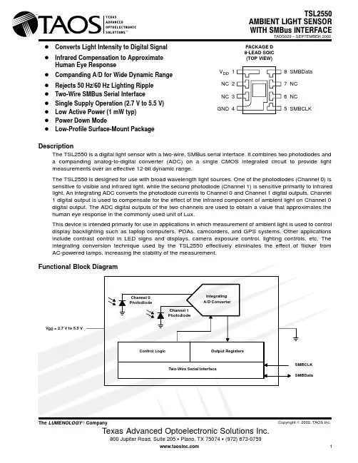
D Converts Light Intensity to Digital Signal D Infrared Compensation to ApproximateHuman Eye ResponseD Companding A/D for Wide Dynamic Range D Rejects 50 Hz/60 Hz Lighting Ripple D Two-Wire SMBus Serial InterfaceD Single Supply Operation (2.7 V to 5.5 V)D Low Active Power (1 mW typ)D Power Down ModeDLow-Profile Surface-Mount PackageDescriptionThe TSL2550 is a digital light sensor with a two-wire, SMBus serial interface. It combines two photodiodes and a companding analog-to-digital converter (ADC) on a single CMOS integrated circuit to provide light measurements over an effective 12-bit dynamic range.The TSL2550 is designed for use with broad wavelength light sources. One of the photodiodes (Channel 0) is sensitive to visible and infrared light, while the second photodiode (Channel 1) is sensitive primarily to infrared light. An integrating ADC converts the photodiode currents to Channel 0 and Channel 1 digital outputs. Channel 1 digital output is used to compensate for the effect of the infrared component of ambient light on Channel 0digital output. The ADC digital outputs of the two channels are used to obtain a value that approximates the human eye response in the commonly used unit of Lux.This device is intended primarily for use in applications in which measurement of ambient light is used to control display backlighting such as laptop computers, PDAs, camcorders, and GPS systems. Other applications include contrast control in LED signs and displays, camera exposure control, lighting controls, etc. The integrating conversion technique used by the TSL2550 effectively eliminates the effect of flicker from AC-powered lamps, increasing the stability of the measurement.8 SMBData 7 NC 6 NC 5 SMBCLKPACKAGE D 8-LEAD SOIC (TOP VIEW)V DD 1NC 2NC 3GND 4Terminal FunctionsAvailable OptionsAbsolute Maximum Ratings over operating free-air temperature range (unless otherwise noted)†. . . . . . . . . . . . . . . . . . . . . . . . . . . . . . . . . . . . . . . . . . . . . . . . . . . . . . . . . . . . .Supply voltage, V DD (see Note 1) 6 V Digital output voltage range, V O–0.3 V to +6 V. . . . . . . . . . . . . . . . . . . . . . . . . . . . . . . . . . . . . . . . . . . . . . . . . . . .. . . . . . . . . . . . . . . . . . . . . . . . . . . . . . . . . . . . . . . . . . . . . . . . . . . . . . . . . . . . . . . . .Digital output current, I O±10 mA. . . . . . . . . . . . . . . . . . . . . . . . . . . . . . . . . . . . . . . . . . . . . . .SMBus input/output current, I(SMBIN)–1 mA to 20 mA. . . . . . . . . . . . . . . . . . . . . . . . . . . . . . . . . . . . . . . . . . . .Operating free-air temperature range, T A –25°C to 85°C. . . . . . . . . . . . . . . . . . . . . . . . . . . . . . . . . . . . . . . . . . . . . . . . . . . .Storage temperature range, T stg –25°C to 85°C. . . . . . . . . . . . . . . . . . . . . . . . . . . . . . . . . . . . . . . . . . . . . . . . . . . . . . . .ESD tolerance, human body model 2000 V †Stresses beyond those listed under “absolute maximum ratings” may cause permanent damage to the device. These are stress ratings only, and functional operation of the device at these or any other conditions beyond those indicated under “recommended operating conditions” is not implied. Exposure to absolute-maximum-rated conditions for extended periods may affect device reliability.NOTE 1:All voltages are with respect to GND.Recommended Operating ConditionsElectrical Characteristics over recommended operating free-air temperature range (unless otherwise noted)Operating Characteristics, V DD = 3.3 V, T A = 255C (unless otherwise noted) (see Notes 2, 3, 4)and infrared 940 nm LEDs are used for final product testing for compatibility with high volume production.3.The 640 nm irradiance E e is supplied by an Al I nGaP light-emitting diode with the following characteristics: peak wavelengthλp = 640 nm and spectral halfwidth ∆λ½ = 17 nm.4.The 940 nm irradiance E e is supplied by a GaAs light-emitting diode with the following characteristics: peak wavelengthλp = 940 nm and spectral halfwidth ∆λ½ = 40 nm.5.The sensor Lux is calculated using the empirical formula shown on p. 12 of this data sheet based on measured Ch0 and Ch1 ADCcount values for the light source specified. Actual Lux is obtained with a commercial luxmeter. The range of the (sensor Lux) / (actual Lux) ratio is estimated based on the variation of the 640 nm and 940 nm optical parameters. Devices are not 100% tested with fluorescent or incandescent light sources.AC Electrical Characteristics, V= 3.3 V, T = 255C (unless otherwise noted)PARAMETER MEASUREMENT INFORMATIONSMBDATASMBCLKStartConditionStop ConditionPSMBDATAt SMBCLKPSSFigure 1. SMBus Timing DiagramsStart byFrame 1 SMBus Slave Address Byte Frame 2 Command ByteACK by Stop by ACK by Figure 2. SMBus Timing Diagram for Send Byte FormatStart by MasterFrame 1 SMBus Slave Address Byte Frame 2 Data Byte From TSL2550ACK by Stop by MasterNACK by Figure 3. SMBus Timing Diagram for Receive Byte FormatTYPICAL CHARACTERISTICSSPECTRAL RESPONSIVITYλ – Wavelength – nmFigure 404000.20.40.60.8150060070080090010001100R e l a t i v e R e s p o n s i v i t yFigure 5NORMALIZED ADC OUTPUTvs.SUPPLY VOLTAGEV DD – Supply Voltage – VN o r m a l i z e d A D C O u t p u t2.533.544.555.560.20.40.60.811.21.41.61.8PRINCIPLES OF OPERATIONAnalog-to-Digital ConverterThe TSL2550 contains an integrating analog-to-digital converter (ADC) that integrates a photodiode current.First it integrates channel 0 photodiode current and then it integrates channel 1 photodiode current. At the end of the conversion cycle for each channel (approximately 400 ms), the conversion result is transferred to the appropriate channel 0 or channel 1 ADC register. The transfer is double-buffered to ensure that invalid data is not read during the transfer. After the data is transferred, the TSL2550 automatically begins the next conversion cycle. Approximately 800 ms is required for both Channel 0 and Channel 1 ADC registers to be updated. A VALID bit is used to indicate that data has been written to the ADC register after ADC is enabled.Interface to the ADC and control of other device functions is accomplished using the standard 2-wire System Management Bus (SMBus) interface. Both versions 1.1 and 2.0 of the SMBus are supported.Digital InterfaceThe TSL2550 contains an 8-bit command register that can be written and read via the SMBus. The command register controls the overall operation of the device. There are two read-only registers that contain the latest converted value of each of the two ADC channels. The SMBus slave address is hardwired internally as 0111001 (MSB to LSB, A6 to A0).Both the send byte protocol and the receive byte protocol are implemented in the TSL2550. The send byte protocol allows single bytes of data to be written to the device (see Figure 6). The written byte is called the COMMAND byte. The receive byte protocol allows single bytes of data to be read from the device (see Figure7). The receive data can be either the previously written COMMAND byte or the data from one of the ADCchannels.S = Start Condition P = Stop Condition Shaded = Slave TransmissionFigure 6. Send Byte ProtocolS = Start Condition P = Stop Condition Shaded = Slave TransmissionFigure 7. Receive Byte ProtocolCommand RegisterThe command register contains eight bits as described in Table 1 and defaults to 0 (0x00) at power-up. A command summary appears in Table 2.Table 1. Command Register Data FormatThe command register is used primarily to select which register will be read during a read cycle (RSEL) and to control the power consumption of the device (ADCEN and PON). When ADCEN and PON are high, the device is in the full powered-up state and is fully operational. When ADCEN and PON are low, both the ADC and the internal oscillator are powered down, resulting in minimum power consumption. Both ADCEN and PON should always be asserted and de-asserted together. The remaining bits (B4, B3, and B2) in the command register should always be written 0. For details on using the command register, see the Operation section, below.Table 2. Command SummaryADC RegisterThe TSL2550 contains two ADC registers (channel 0 and channel 1). Each ADC register contains two components to determine the logarithmic ADC count value: CHORD bits and STEP bits. The CHORD bits correspond to the most significant portion of the ADC value and specifies a segment of the piece-wise linear approximation. The STEP bits correspond to the least significant portion of the ADC count value and specifiesa linear value within a segment. CHORD and STEP bits all equal to 0 corresponds to a condition in which thelight level is below the detection limit of the sensor. CHORD and STEP bits all equal to 1 corresponds to an overflow condition.Each of the two ADC value registers contain seven bits as described in T able 3. The specific ADC value register read depends on the last written RSEL field to the command register, as described above and in the Operation section, below.Table 3. ADC Register Data FormatThe MSB of the ADC register (VALID bit B7) is used to indicate that data has been written to the ADC register after the ADC and internal oscillator are activated as described in Command Register section.Bits 6 through 0 contain the 7-bit code representing the ADC count value, which is proportional to a photodetector current. In this code, the ADC count value is represented by a piece-wise linear approximation to a log function. The transfer function is broken into 8 chords of 16 steps each. (This code is very similar to µ-law code used in audio compression — it differs in that it does not have a sign bit and it is not inverted.) T able 4 shows the relationship between the CHORD and STEP bits and the CHORD and STEP numbers and values. These are used to calculate the ADC count value.Table 4. CHORD and STEP Numbers and Values vs Register BitsNOTES: A.CHORD VALUE = INT (16.5 × ((2C) – 1))B.STEP VALUE = 2CThe ADC count value is obtained by adding the CHORD VALUE and the product of the STEP NUMBER and STEP VALUE (which depends on CHORD NUMBER).ADC Count Value+((Chord Value))(Step Size)(Number of Steps)) The ADC count value is as a formula:ADC Count Value+(INT(16.5((2C*1))))(S(2C))where:C is the CHORD NUMBER (0 to 7)S is the STEP NUMBER (0 to 15)as defined in Table 4.OperationAfter applying VDD, the device will initially be in the power down state. To operate the device, issue an SMBus Send Byte protocol with the device address and the appropriate command byte to read ADC channel 0 or ADC channel 1 (see T able 2). T o obtain the conversion result, issue an SMBus Receive Byte protocol with the device address. The data byte received will correspond to the value in the ADC register (0 or 1) specified by the previous command. If a conversion has not been completed since power up (either through V DD or ADCEN/PON), the valid bit will be 0, and the data will not be valid. If there is a valid conversion result available, the valid bit will be set (1), and the remaining 7 bits will represent valid data from the previously selected ADC register. Data may be read repeatedly from the currently selected ADC register, and although it will remain valid, the ADC register will not be updated until a new conversion completes for that channel (800 ms total since there are two serial 400 ms per channel conversion times). Note also that the command register itself may be read, as a check to be sure that the device is communicating properly.To power down the device for reduced power consumption, issue an SMBus Send Byte protocol with the device address followed by 0 to clear the ADCEN and PON bits.APPLICATION INFORMATIONThe TSL2550 is intended for use in ambient light detection applications, such as display backlight control, where adjustments are made to display brightness or contrast based on the brightness of the ambient light, as perceived by the human eye. Conventional silicon detectors respond strongly to infrared light, which the human eye does not see. This can lead to significant error when the infrared content of the ambient light is high, such as with incandescent lighting, due to the difference between the silicon detector response and the brightness perceived by the human eye.This problem is overcome in the TSL2550 through the use of two photodiodes. One of the photodiodes (Channel0) is sensitive to both visible and infrared light, while the second photodiode (Channel 1) is sensitive primarilyto infrared light. An integrating ADC converts the photodiode currents to Channel 0 and Channel 1 digital outputs. Channel 1 digital output is used to compensate for the effect of the infrared component of light on the Channel 0 digital output. The ADC digital outputs from the two channels are used in a formula to obtain a value that approximates the human eye response in the commonly used Illuminance unit of Lux:Light Level(lux)+(Ch0Counts)(0.46)(e(*3.13R))where:R = (Ch1 Counts) / (Ch0 Counts)The formula above was obtained by optical testing with fluorescent and incandescent light sources. The light level calculated from the formula will be slightly higher than the actual light level for sunlight and will be slightly lower than the actual light level for composite fluorescent and incandescent light sources.Table 5 contains a summary of the typical sensor outputs for several common light sources.Table 5. Sensor Output SummaryLight from 50 or 60 Hz sources, and especially fluorescent lighting, has a high harmonic content. Since the TSL2550 integrates the ambient light over an approximately 400 millisecond interval (per channel), this light ripple is typically reduced to less than ¼ LSB.Power Supply DecouplingThe power supply lines must be decoupled with a 0.1 µF capacitor placed as close to the device package as possible. The bypass capacitor should have low effective series resistance (ESR) and effective series inductance (ESI), such as the common ceramic types, which provide a low impedance path to ground at high frequencies to handle transient currents caused by internal logic switching.MECHANICAL DATAPACKAGE DPLASTIC SMALL-OUTLINEDETAIL AA2y 6y 1.8 +NOTES: A.All linear dimensions are in millimeters.B.Package is molded with an electrically nonconductive clear plastic compound having an index of refraction of 1.55.C.Actual product will vary within the mechanical tolerances shown on this specification. Designs for use of this product MUST allowfor the data sheet tolerances.D.This drawing is subject to change without notice.PRODUCTION DATA — information in this document is current at publication date. Products conform to specifications in accordance with the terms of Texas Advanced Optoelectronic Solutions, Inc. standard warranty. Production processing does not necessarily include testing of all parameters.NOTICETexas Advanced Optoelectronic Solutions, Inc. (TAOS) reserves the right to make changes to the products contained in this document to improve performance or for any other purpose, or to discontinue them without notice. Customers are advised to contact TAOS to obtain the latest product information before placing orders or designing TAOS products into systems. TAOS assumes no responsibility for the use of any products or circuits described in this document or customer product design, conveys no license, either expressed or implied, under any patent or other right, and makes no representation that the circuits are free of patent infringement. TAOS further makes no claim as to the suitability of its products for any particular purpose, nor does TAOS assume any liability arising out of the use of any product or circuit, and specifically disclaims any and all liability, including without limitation consequential or incidental damages.TEXAS ADVANCED OPTOELECTRONIC SOLUTIONS, INC. PRODUCTS ARE NOT DESIGNED OR INTENDED FOR USE IN CRITICAL APPLICATIONS IN WHICH THE FAILURE OR MALFUNCTION OF THE TAOS PRODUCT MAY RESULT IN PERSONAL INJURY OR DEATH. USE OF TAOS PRODUCTS IN LIFE SUPPORT SYSTEMS IS EXPRESSLY UNAUTHORIZED AND ANY SUCH USE BY A CUSTOMER IS COMPLETELY AT THE CUSTOMER’S RISK.LUMENOLOGY is a registered trademark, and TAOS, the TAOS logo, and Texas Advanced Optoelectronic Solutions are trademarks of Texas Advanced Optoelectronic Solutions Incorporated.。