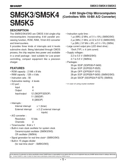
DESCRIPTIONThe SM5K3/5K4/5K5 are CMOS 4-bit single-chip microcomputers incorporating 4-bit parallel pro-cessing function, ROM, RAM, 10-bit A/D converter and timer/counters.It provides three kinds of interrupts and 4 levels subroutine stack. Being fabricated through CMOS process, the chip requires less power and available in a small package : best suitable for Low power controlling, compact equipment like a precision charger.FEATURES• ROM capacity : 2 048 x 8 bits• RAM capacity : 128 x 4 bits• Instruction sets : 50• Subroutine nesting : 4 levels• I/O port :Input8Output4Input/output12 (36QFP/32SOP)11 (30SDIP)8 (28SOP)• Interrupts :Internal interrupt x 1 (timer)External interrupt x 2 (2 external interruptinputs)• A/D converter :Resolution10 bitsChannels4• Timer/counter : 8-bit x 1• Built-in main clock oscillator for system clock Ceramic/crystal oscillator (SM5K3/5K5)CR oscillator (SM5K4)• Signal generation for real time clock∗(SM5K3/5K5)• Built-in 15 stages divider(for real time clock∗: SM5K3/5K5)• Instruction cycle time :1 µs (MIN.) (2 MHz, at 5 V ±10%) (SM5K3/5K5)2 µs (MIN.) (1 MHz, at 2.2 to 5.5 V) (SM5K3/5K5)1 µs (MIN.) (1.67 MHz ±20%, at 5 V ±10%) (SM5K4)• Large current output pins (LED direct drive) : 15mA (TYP.)x 4 (sink current)• Supply voltages:2.2 to 5.5 V (SM5K3/5K5)2.7 to 5.5 V (SM5K4)• Packages :30-pin SDIP (SDIP030-P-0400)32-pin SOP (SOP032-P-0525)36-pin QFP (QFP036-P-1010)28-pin SOP (SOP028-P-0450) (SM5K3/5K5)24-pin SSOP (SSOP024-P-0275) (SM5K4)∗In case of using crystal oscillatorSM5K3/SM5K4 SM5K54-Bit Single-Chip Microcomputers (Controllers With 10-Bit A/D Converter)In the absence of confirmation by device specification sheets, SHARP takes no responsibility for any defects that may occur in equipment using any SHARP devices shown in catalogs, data books, etc. Contact SHARP in order to obtain the latest device specification sheets before using any SHARP device.NomenclatureA : A registerA/D : A/D converter unitALU : Arithmetic logic unitB M, B L: RAM address registerC : Carry flagIFA, IFB, IFT : Interrupt request flagIME : Interrupt master enable flag INST. DEC. : Instruction decoder INT : Interrupt control unit P0-P5 : Port registerP U, P L: Program counterR8, R9, RC, RE, RF : Mode registerRA : Count registerRB : Modulo registerSB : SB registerSR : Stack registerRECOMMENDED OPERATING CONDITIONSNOTES :• The typical oscillation frequency shall be determined in consideration of operating condition and fluctuation frequency.• Mount Rf, RD, C 1, C 2, Oscillator (SM5K3/5K5)/Rf (SM5K4)as close as possible to the oscillator pins of the LSI, in order to reduce an influence from floating capacitance.• Since the value of resistor Rf, RD, C 1, C 2, Oscillator (SM5K3/5K5)/Rf (SM5K4) varies depending on circuit pattern and others, the final Rf, RD, C 1, C 2, Oscillator (SM5K3/5K5)/Rf (SM5K4) value shall be determined on the actual unit.• Don't connect any line to OSC IN and OSC OUT except oscillator circuit.• Don't put any signal line across the oscillator circuit line.• On the multilayer circuit, do not let the oscillator circuit wiring cross other circuit.• Minimize the wiring capacitance of GND and V DD .OSCILLATION CIRCUITDegree of fluctuation frequency : ±20%OSC OUTOSC INRf = 33 k Ω(fosc = 1.67 MHz, TYP.)• SM5K3/5K5∗Reference only : Circuit configuration varies according tooscillator used.• SM5K4C 2NOTES :1. Applicable pins : P12, P13, P20-P23, P30-P33(digital inputmode), P40-P43P50-P532. Applicable pins : OSC IN , RESET, P10, P113. Applicable pins : RESET, P10-P13, P20-P23, P40-P43,P50-P53 (digital input mode)4. Applicable pins : P30-P33(analog input mode)03(high current mode)6. Applicable pins : P20-P23, P40-P43, P50-P53(output mode)∗17. Applicable pins : P30-P33∗28. No load (A/D conversion is stop.)9. A/D conversion in operation (operation enable)10. A/D conversion in stop (operation disable)∗1 In case of 32-pin SOP and 36-pin QFP.(In case of 30-pin SDIP, P52dose not exist. In case of 28-pin SOP, P50-P53do not exist.)∗2 P3 ports are normally used for input ports with pull-up resistor. These ports can be also used.V IH10.8 x V DDV DDV 1V IL100.2 x V DDV IH20.9 x V DDV DDV 2V IL200.1 x V DDV DD = 2.2 to 3.3 V 22590I IL1V IN = 0 V V DD = 4.5 to 5.5 V 2570250µA 3I IH1V IN = V DD 2I IL2V IN = 0 V 1.010µA4I IH2V IN = V DD 1.010V DD = 2.2 to 3.3 V 515I OL1V O = 1.0 V V DD = 4.5 to 5.5 V 1525mA 5V DD = 2.2 to 3.3 V 0.3 1.5I OH1V O = V DD – 0.5 V V DD = 4.5 to 5.5 V 1.0 2.2V DD = 2.2 to 3.3 V 1.2 5.0I OL2V O = 1.5 V V DD = 4.5 to 5.5 V 59.0mA 6V DD = 2.2 to 3.3 V 0.3 2.0I OH2V O = V DD – 0.5 V V DD = 4.5 to 5.5 V 1.0 2.4V DD = 2.2 to 3.3 V 0.15I OH3V OH = V DD – 1.0 V mA7V DD = 4.5 to 5.5 V 0.5f OSC = 2 MHZ V DD = 4.5 to 5.5 V 1 200 2 500V DD = 2.2 to 3.3 V 300800f OSC = 1 MHzI DDV DD= 4.5 to 5.5 V 600 1 200f OSC = 32.768 kHzV DD= 2.2 to 3.3 V 20120(Crystal OSC mode)f OSC = 2 MHzV DD = 4.5 to 5.5 V 760 1 500V DD= 2.2 to 3.3 V 200600µA8f OSC = 1 MHzI HLT V DD = 4.5 to 5.5 V 400900f OSC = 32.768 kHzV DD= 2.2 to 3.3 V 2075(Crystal OSC mode)Ceramic OSC mode V DD= 2.2 to 3.3 V 2I STOP f OSC = 32.768 MHzV DD= 2.2 to 3.3 V 1540(Crystal OSC mode)A/D in operation V DD = 4.5 to 5.5 V 220450µA 9I VRA/D in stopV DD = 4.5 to 5.5 V 2µA 10Resolution 10bit Differential f OSC = 1 MHzV DD= VR = 5.0 V ±2.5±4.0linearity error T OPR = 25°CSequential f OSC = 1 MHzV DD = VR = 5.0 V ±3.2±5.0LSB linearity error T OPR = 25°Cf OSC = 1 MHzTotal error V DD= VR = 5.0 V±4.0±6.0TOPR = 25°CA/D conversion Input voltage Input currentOutput currentSupply cerrentDC CHARACTERISTICS• SM5K3(T OPR = –20 to +70°C, TYP. value : V DD = 5.0 or 3.0 V, Unless otherwise noted.)PARAMETER SYMBOLCONDITIONSMIN.TYP.MAX.UNIT NOTE1. Applicable pins:P12, P13, P20-P23, P30-P33(digital inputmode), P40-P43, P50-P53∗12. Applicable pins:OSC IN0, P113. Applicable pins:RESET, P10-P13, P20-P23, P40-P43,P50-P53(digital input mode)∗14. Applicable pins:P30-P33(analog input mode)5. Applicable pins:P00-P03(high current output)6. Applicable pins:P20-P23, P40-P43, P50-P53(output mode)∗17. Applicable pins:P30-P33∗29. A/D conversion in operation (A/D conversion enable)10. A/D conversion in stop (A/D conversion disable)∗1 In case of 32-pin SOP and 36-pin QFP.(In case of 30-pin SDIP, P52pin dose not exist. In case of 24-pin SSOP, P12, P13, P33, P50-P53pins do not exist.)∗2 P3 ports are normally used for input port with pull-up resistor. These ports can be also used as a suspected case of output port.Data Memory (RAM)The data memory (RAM) is used to store data upFig. 3 B Register and SB RegisterFig. 4 RAM File and WordB Register and SB Register• B register (B M , B L )The B register is an 8-bit register that is used to specify the RAM address. The upper 4-bit section is called B M register and lower 4-bit B L .• SB registerThe SB register is an 8-bit register used as the save register for the B register. The contents of B register and SB register can be exchanged throughEX instruction.The program counter PC specifies the ROM address. The PC consists of 12-bit as shown in Fig. 5 : The upper 6-bit (P U ) represents a page while the lower 6-bit (P L ) denotes a step. The P U section is a register and the P L section, a binary counter.Execution of interrupt handling and the table reference instruction PAT also automatically uses 1stage of the stack register SR.Program Memory (ROM)The ROM is used to store the program. The capacity of the ROM is 2 048-step (32-page by 64-step. See Fig. 6). The configuration of the ROM and program jumps are illustrated in Fig. 7.Fig. 6 Page and Step for ROMFig. 5 Program Counter PC and Stack Register SRProgram Counter PC and Stack Register SRFig. 7 ROM Configuration and Program Jump ExampleOutput Latch Register and Mode RegisterThe SM5K3/5K4/5K5 contain 6 output-latch registers and 8 mode-registers which either latch contents of output ports or control some functions of the SM5K3/5K4/5K5.These registers, their functions and available transfer instructions are shown in Table 1 below.An output latch register sets the output level of the pin to which it is connected.Refer to the section of “MODE REGISTERS”concerning about the details mode registers.Table 1 Output Latch Registers and Mode RegistersNOTE :Bit 4 (R84) in the R8 register is read only.(Read or write operation of this bit does not affect any other operation.)FUNCTIONAL DESCRIPTION Hardware Reset FunctionReset function initializes the SM5K3/5K4/5K5systems. When the input on the RESET pin goes Low, the system enters reset condition after 2level, the reset condition is removed as the inputpulse from OSC IN pin repeats 215times, forcing the program counter to start at 0 page and 0 address.Initialized status of the system immediately after resetting is shown below.Reset causes the following changes.1) I/O pins are set input.2) All mode registers are reset.3) Output latch register P0 is reset, causing P00to P03pins go High level.4) Interrupt request flags (IFA, IFB, and IFT),interrupt master enable flag (IME) are reset,disabling all interrupts.Standby FeatureThe standby function saves power by stopping the program whenever it is not necessary to run. The mode in which the microcomputer is executing the program is called the run mode and the mode in which it stops the program is called the standby mode. Standby mode is further divided into two modes : stop mode and halt mode, one of which is selected by halt instruction or stop instruction. Upon removal of standby condition, the SM5K3/5K4/5K5return from the standby mode to the normal run mode. To enter the standby mode, select either stop mode or halt mode whichever is appropriate (Fig. 8).∗The content of the bit R84 is undefined because it is read only.• Blocks stopped during standby modeIn the halt modeThe system clock generating circuit stops during the halt mode, deactivating all the blocks driven by the system clock. The main clock and dividers remain active. This means that timers can be used while in the halt mode. Both internal and external clocks can be used as the count clock.In the stop modeThe main clock and system clock stop upon entering the stop mode. Therefore, only timers using the external clock remain active.• Counters that the system retains during standby modeThe contents that will be retained in the halt mode will also be retained in the stop mode. These items are shown in Table 3.Fig. 8 Operation Shift of Program• Releasing events of standby mode (6-type)• Interrupt used with SM5K3/5K4/5K5Interrupt event occurs on the falling edge of P10or P11pin input, or the overflow at the timer. These events set flags IFA, IFB and IFT respectively, that then serve as interrupt request flag.Table 4 shows interrupt handling priority level and jump address.• Usage of halt mode and stop modeThe system returns back to the normal operation mode upon occurring of a standby mode releasing condition. The halt mode should be used when the system must enter and exit normal operation frequently as in the case of key operation.The halt mode should also be used to keep timers that are operating from the internal clock, while in the standby mode.The stop mode further saves power than the halt mode but requires slightly longer time to return tothe normal mode. Therefore, the stop mode should be used when the system will not be required to return to the normal mode in a short time.Interrupt FeatureThe interrupt block consists of mask flags (bits RE0,RE1 and RE2), IME flag and interrupt request handling circuit. Fig. 9 shows the configuration of the interrupt block.Fig. 9 Interrupt Block Diagram• IME flag (master enable flag)The IME enables or disables all interrupts at the same time. The IE command, when executed, sets the IME flag and enables the interrupt specified by the mask flag setting. The ID command resets the IME flag, disabling process of any interrupt request.Setting the IME flag to reset after releasing hardware reset, all interrupts are inhibited.• Mode register RE (interrupt mask flag)The mode register RE (RE0, RE1 and RE2;interrupt mask flag) individually enables or disables three type of interrupts.Timer/CounterThe SM5K3/5K4/5K5 have a pair of built-in timer/counter. The timer/counter are used to handle periodic interrupts and to count. The overflowing timer can be used to disable the halt mode. The timer/counter serve as interval timer.The timer/counter consists of an 8-bit count register RA, modulo register RB (for counter initial value setting), 15-bit divider and 4-bit mode register RC (for count clock selection). The configuration of the timer/counter is shown in Fig. 10.Fig. 10 Configuration of Timer/Counter• Selecting count clockA count clock is selected by the bit settings in the mode register RC.Table 5 Count Clock SelectionA/D CONVERSION MODEIn the A/D conversion mode, the converter converts the analog input voltage to the digital value. The analog input voltage is successively compared with the internal voltage charged on the weighted capacitor array until its digital equivalent is determined. The resultant digital data is stored into the mode registers R8 and R9.The conversion requires 152.5 µs (main clock at 400 kHz/system clock at 5 µs) or 1.86 ms (main clock at 32.768 kHz/system clock at 61 µs).COMPARISON MODEIn the comparison mode, the analog voltage from one of P30to P33pins is compared, in amplitude, with internally generated voltage whose value is set by the mode registers R8 and R9. The result data of the comparison is saved into the bit 4 (bit R84) position of the mode register R8. The comparison cycle lasts 62.5 µs (main clock at 400 kHz, system clock at 5 µs) or 763 µs (main clock at 32.768 kHz/system clock at 61 µs).A/D ConversionThe SM5K3/5K4/5K5 are provided with a built-in 10-bit A/D converter having 4-channel multiplexer analog inputs. The A/D converter operates in A/D conversion mode and comparison mode. In the A/D conversion mode, the converter converts the analog input from the P3 pin to the digital value; and in the comparison mode, it compares the input analog amplitude with that of a reference voltage set inside the SM5K3/5K4/5K5. The P30to P33 pins can be used as analog voltage inputs. One or more of these 4 inputs can be set to assume A/D pin by the bit operation of the mode register R3. One of these A/D pins is further set as analog input by the bit operation of the mode register R8. The A/D converter is controlled by the bits set in the mode register R8. For details of the mode register R8, refer to " MODE REGISTERS R8 ". Configuration of the A/D converter is illustrated in Fig. 11.CAUTIONS• Keep the A/D converter reference voltage on the VR pin equal to or below V DD.• Do not apply the voltage to the VR pin before V DD is applied.• Connect AGND to GND.Fig. 11 A/D Converter Block DiagramMODE REGISTERSThe registers which control functions of the SM5K3/5K4/5K5 and which serve as counter/timer are commonly referred to as “mode registers”. In the SM5K3/5K4/5K5, R8 to RB are 8-bit mode registers;and R3, RC, RE and RF are 4-bit mode registers.To set data into the mode registers, the OUT command is used; and to check the contents of the mode registers IN command is used.R3 (A/D pin selection register)Any pin on 4-pin port P3 can be set accommodate analog voltage (hereafter called A/D pin).Bit i (i = 3 to 0)Sets P3i pin to either general purpose input or A/D pin0 | (General purpose) input 1 | A/D inputR8 (A/D conversion control & A/D data register)An 8-bit register used to control A/D conversion and storing part of A/D conversion result. It also stores the results of comparison.Bits 7 to 6Storage of A/D conversion result (A/D conversion mode) and setting of internal voltage (comparison mode)• Use as part of a 10-bit data ragister in combination with mode register R9.• Bit R86 is the LSB.• Store lower 2-bit of converted data in A/D conversion mode.• Use as lower 2-bit of internal voltage setting data in comparison mode.Bit 5∗A/D operation enable/disable flag 0 | Disable (A/D power source off)1 | Enable (A/D power source on)Bit 4Storages of comparison result (read only)0 | P3i pin voltage < internal setting voltage 1 | P3i pin voltage > internal setting voltage(i = 3 to 0)Bit 3∗S/R flag (start/clear)0 | End of operation (or stop)1 | Start of operation (or in operation)Bit 2Operation mode selection 0 | A/D conversion 1 | Comparison Bits 1 to 0Select one of A/D pins as A/D conversion 00 | P3001 | P3110 | P3211 | P33R9 (A/D data register)The register to store the upper 8-bit of 10-bit data resulting from A/D conversion.Bit 7Bit i (i = 7 to 0)Storages of A/D conversion result (A/D conversion mode) and setting of internal voltage (comparison mode)• Uses as part of a 10-bit data register in combination with mode register R8.• Bit R97 is the MSB.• Stores upper 8-bit of A/D conversion result.• Uses as upper 8-bit of internal voltage setting data in comparison mode.∗When operation is end, these bits are cleared.∗Select one pin which is to be selected by mode register R8.RA (Count register)Bit i (i = 7 to 0)Count clock input register• Uses as counter part of timer/counter (count clock input).• Loads the content of RB to RA when the RAoverflows or when OUT command (B L = 0A H )is executed.RA ←RB• Loads the content of RA to X and A registers upon execution of IN command (B L = 0A H ).(X, A)←RA• Bit 7 = MSB, bit 0 = LSBRB (Modulo register)Bit i (i = 7 to 0)Count initial value storage register• Uses as modulo register of timer/counter • Loads the content of RB to X and A registers upon execution ofIN command (B L = 0B H ) : X = upper bits,A = lower bits.(X, A)←RB• Loads the contents of X and A registers to RB upon execution ofOUT command (B L = 0B H ) :X = upper bits,A = lower bits.RB ←(X, A)• Bit 7 : MSB, Bit 0 : LSBRC (Timer control)Bit 3Starts up count of the timer.0 | Stop 1 | StartBit 2 (Unused)Bits 1 to 0Select the source clock to the timer.00 | f SYS (system clock)01 | f SYS /2710 | f SYS /21511 | Falling edge input on P11pinRE (Interrupt mask flag)Bit 3Bit 3 (Unused)Bit 2Removes overflow interrupt from timer or standby condition.0 | Disable 1 | Enable Bit 1Interrupts on the falling edge of input from P11 pin,or releases of standby mode by the Low input from P11pin.0 | Disable 1 | Enable Bit 0Interrupts on the falling edge of input on P10pin, or releases of standby mode by the Low input from P10pin.0 | Disable 1 | EnableRF (P2 port direction register)Bit 3Bit i (i = 3 to 0)Selection of input pin/output pin 0 | Set P2i pin to input.1 | Set P2i pin to output.I/O PortsThe SM5K3/5K4/5K5 have 24 ports : 8-input, 4-output and 12-I/O port. To verify the input, use suitable instruction to transfer the input on the pin directly to the A register. To select the output latch register to which the content of the A register is to be transferred, and to select the input port from which the signal or data is to be transferred to the A register, use the B L register. For details of B L settings and associated ports, refer to Table 1.• Port P00to P03(CMOS inverting output port) The data transfers in 4-bit string (use OUT or OUTL instruction) or in unit of 1-bit (use ANP or ORP instruction).• Port P10to P13(input port with pull-up resistor) The data transfers in unit of 4-bit. This port can be used as standby/external interrupt input or count pulse input. The P1 port can also be used as a standby release port without requiring specific setting on P12and P13pins. Pins P10and P11 require settings through the mode resister RE. When using the P1 port as an external interrupt input, use pins P10and P11with suitable settings in the mode register RE. When using the P1 port as the count pulse input, use P11pin.• Port P20to P23(I/O port with pull-up resistor) Each bit can be independently be set its direction and can be transferred independently or in combination of other 3-bit. The direction of the bits is determined by the RF register. After reset, the P2 port is set input.• Port P30to P33(input port with pull-up resistor) The data transfers in unit of 4-bit. The port can also be used as A/D analog voltage input. To use the P3 port as the A/D port, set the mode register R3.• Port P40to P43(I/O port with pull-up resistor) The data transfers in unit of 4-bit.When set output, content of each bit can be set. Executing the input instruction (IN) sets the P4 ports (P40to P43) to input; and executing output instruction (OUT, ANP or ORP) sets the port to output. After reset, the P4 port is set input.• Port P50to P53(I/O port with pull-up resistor) The data transfers in unit of 4-bit.When set output, content of each bit can be set. Executing the input instruction (IN) sets the P5 ports (P50to P53) to input; and executing output instruction (OUT, ANP or ORP) sets the port to output. After reset, the P5 port is set input.FlagsThe SM5K3/5K4/5K5 have 4 flags (C flag and interrupt request flags [IFA, IFB, IFT] ), which are used to perform setting and judgments.• DividerThe divider consists of 15 divided-by-two dividers,providing 2 (f SYS /27, f SYS /215) of 4 count clocks that are fed to the counter RA from the system clock.Its configuration is shown below. The divider can be cleared by using the DR instruction.• Oscillator mask optionSelection of type of oscillator, ceramic or crystal, is made by mask option.Fig. 12 Main Clock and System ClockFig. 13 System Clock Generator and DividerSystem Clock Generator and Dividers• System clock generatorThe system clock is the divided-by-two main clock applied through OSC IN and OSC OUT (See Fig. 12).The system clock generator is shown in Fig. 13.One system clock cycle period is equal to one instruction execution time when the instruction consists of 1 word. When the ceramic oscillatorruns at 400 kHz, the system clock fsys is 200 kHz.This means that the instruction execution time is 5µs/word. Using a 32.768 kHz crystal oscillator generates 16.384 kHz fsys and the instruction execution time is 61 µs/word. The system clock can be used as count input pulse to the timer.INSTRUCTION SET Array Definition of SymbolsM: Content of RAM at the address defined by the B register.←: Transfer direction∪: Logical OR∩: Logical AND⊕: Exclusive ORAi: An i bit of A register (i = 3 to 0)Push: Saves the contents of PC to stack register SR.Pop: Returns the contents saved in the stack register back to PC.Pj: Indicates output latch register or input register. Pj ( j = 0, 1, 2, 3, 4, 5)Rj: Mode register. Rj register ( j = 3, A, B, C, E, F)ROM ( ) : Content stored in ROM location defined by the value in ( ).CY: Carry in ALU (independent of C flag) The CY(carry) is a signal which isgenerated when the ALU has beencarried by the execution of a command.It is different from the C flag.X: Used to represent a group of bits in the content of a register or memory. Forexample, the X in the LDAX instructiondenotes the lower 2 digits (I1and I0) of Aregister.• A bit in a register is affixed to the register symbol, e.g. a bit (i = 0, 1, 2, 3....) of X register is expressed as Xi and P (R) register as P (R) i.• Increment means binary addition of 1H and decrement addition of F H.• Skipping an instruction means to ignore that instruction and to do nothing until starting the next instruction. In this sense, an instruction to be skipped is treated as an NOP instruction. Skipping 1-byte instruction requires 1-cycle, and 2-byte instruction 2-cycle. Skipping 1-byte 2-cycleinstruction requires 1-cycle.SYSTEM CONFIGURATION EXAMPLE • Charger controller。