电子科技大学15春《数字逻辑设计及应用》在线作业3满分答案
- 格式:doc
- 大小:27.50 KB
- 文档页数:3
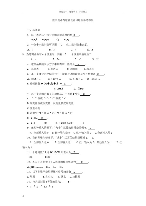
数字电路与逻辑设计习题及参考答案一、选择题1. 以下表达式中符合逻辑运算法则的是 D 。
·C=C 2 +1=10 <1 +1=12. 一位十六进制数可以用 C 位二进制数来表示。
A . 1 B . 2 C . 4 D . 163. 当逻辑函数有n 个变量时,共有 D 个变量取值组合?A. nB. 2nC. n 2D. 2n 4. 逻辑函数的表示方法中具有唯一性的是 A 。
A .真值表 B.表达式 C.逻辑图 D.状态图5. 在一个8位的存储单元中,能够存储的最大无符号整数是 D 。
A .(256)10 B .(127)10 C .(128)10 D .(255)106.逻辑函数F=B A A ⊕⊕)( = A 。
C.B A ⊕D. B A ⊕ 7.求一个逻辑函数F 的对偶式,不可将F 中的 B 。
A .“·”换成“+”,“+”换成“·” B.原变量换成反变量,反变量换成原变量 C.变量不变D.常数中“0”换成“1”,“1”换成“0” 8.A+BC= C 。
A .A+B +C C.(A+B )(A+C ) +C9.在何种输入情况下,“与非”运算的结果是逻辑0。
DA .全部输入是0 B.任一输入是0 C.仅一输入是0 D.全部输入是1 10.在何种输入情况下,“或非”运算的结果是逻辑1。
AA .全部输入是0 B.全部输入是1 C.任一输入为0,其他输入为1 D.任一输入为111.十进制数25用8421BCD 码表示为 B 。
101 010112.不与十进制数()10等值的数或代码为 C 。
A .(0101 8421BCD B .16 C .2 D .813.以下参数不是矩形脉冲信号的参数 D 。
A.周期 B.占空比 C.脉宽 D.扫描期 14.与八进制数8等值的数为: BA. 2B.16C. )16D. 215. 常用的BCD码有 D 。
A.奇偶校验码B.格雷码码 D.余三码16.下列式子中,不正确的是(B)+A=A B.A A1⊕=⊕=A ⊕=A17.下列选项中,______是TTLOC门的逻辑符号。

答案+我名字查看考卷——作业提交1当前得分:15 分(总分:100 分),折合成百分制共 15 分。
返回作业提交11.逻辑函数,请问其反函数 。
()()()[参考答案:] 分值:5 得分:分 系统自动批改于2019年9月19日 14点35分2. 有关异或逻辑的描述不正确的是 。
() 异或逻辑的反函数是同或逻辑 () 异或逻辑的对偶逻辑是同或逻辑() 一个逻辑变量和0异或得到的是其反函数 [参考答案:] 分值:5 得分:分 系统自动批改于2019年9月19日 14点35分3. 已知一个逻辑的最小项之和为F(, , )=∑m(0,4,7) ,以下哪个等式成立。
()()()[参考答案:] 分值:5得分:5分系统自动批改于2019年9月19日14点35分4. 下面所描述的逻辑函数表达式中,哪一种可以直接从真值表中得到,而无需其他中间步骤。
() 标准形式() 最简与或式() 与非-与非形式[参考答案:] 分值:5得分:5分系统自动批改于2019年9月19日14点35分5.下面有关最小项的描述正确的是。
()()()[参考答案:] 分值:5得分:0分系统自动批改于2019年9月19日14点35分6. 下面有关逻辑函数的描述中,正确的是。
() 逻辑函数的最小项之和是唯一的() 逻辑函数的最简与或表达式是唯一的() 逻辑函数的与非-与非逻辑表达式是唯一的[参考答案:] 分值:5得分:5分系统自动批改于2019年9月19日14点35分7. 请问或非逻辑的对偶关系是。
() 或非逻辑() 与非逻辑() 与或非逻辑[参考答案:] 分值:5得分:0分系统自动批改于2019年9月19日14点35分8.逻辑函数,请问其最小项之和为。
()()()[参考答案:] 分值:5得分:0分系统自动批改于2019年9月19日14点35分9. 逻辑函数Y(, , , )=∑m(0,2,4,6,9,13) + (1,3,5,7,11,15)的最简与或式为()() +’’() ’+() +[参考答案:] 分值:5得分:0分系统自动批改于2019年9月19日14点35分10.逻辑函数Y的真值表如下:。

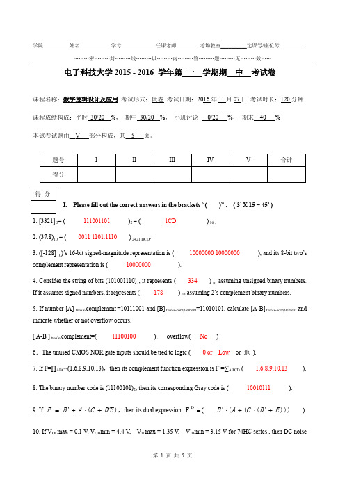
………密………封………线………以………内………答………题………无………效……电子科技大学2015 - 2016 学年第 一 学期期 中 考试卷课程名称:数字逻辑设计及应用 考试形式:闭卷 考试日期:2016年11月07日 考试时长:120分钟 课程成绩构成:平时 30/20 %, 期中 30/20 %, 小班讨论 0/20 %, 期末 40 % 本试卷试题由__V___部分构成,共__5___页。
I. Please fill out the correct answers in th e brackets “( )” . ( 3’ X 15 = 45’ )1. [3321] 5= ( 111001101 )2 = ( 1CD ) 16 .2. (37.8)10 = ( 0011 1101.1110 ) 2421 BCD .3. ([-128] 10)’s 16-bit signed-magnitude representation is ( 10000000 10000000 ), and its 8-bit two’s complement representation is ( 10000000 ).4. Consider the string of bits (101001110)2, it represents ( 334 ) 10 assuming unsigned binary numbers. If it assumes signed numbers, it represents ( -178 ) 10 assuming 2’s complement binary numbers.5. If number [A] two’s -complement =10111001 and [B] two’s -complement =11010101, calculate [A-B] two’s -complement and indicate whether or not overflow occurs.[ A-B ] two’s -complement=( 11100100 ), overflow( No )6.The unused CMOS NOR gate inputs should be tied to logic ( 0 or Low or 地 ).7. If F=∏ABCD (1,6,8,9,10,13),then its complement function expression is F’=∑ABCD ( 1,6,8,9,10,13 ). 8. The binary number code is (11100101)2, then its corresponding Gray code is ( 10010111 ).9. If )(E D C A B F '+⋅+'=,then its dual expression =DF ( )))(((E D C A B +'⋅+⋅' ).10. If V OL max = 0.1 V, V OH min = 4.4 V , V IL max = 1.35 V , V IH min = 3.15 V for 74HC series , then DC noise………密………封………线………以………内………答………题………无………效……margin is V NL = ( 1.25 )V, V NH = ( 1.25 )V.II. Choose the only one correct answer and fill the item number in the brackets. (2’ X 10=20 )1. Which of these four gates is the fastest ? ( C )A. ANDB. ORC. NANDD. NOR2. To Implement this function F=(A’B(D’+C’D)+B(A+A’CD))’(A’B(C+D)’), how many AND gates at least we should use? ( A )A. 0B. 1C. 2D. 33. If we want to use an XOR gate as an Inverter (NOT gate), then the inputs of A and B should connect as the ( A ) .A one of the A andB connect to ‘1’B one of the A and B connect to ‘0’C A and B connect togetherD can’t realize4. The output signal of ( B ) circuit is 1-out-of-M code.A Binary EncoderB Binary DecoderC Seven-Segment DecoderD Multiplexer5.A CMOS circuit is shown as Fig 1,its’ logic function F =(B). (positive logic).A A⋅B+C⋅DB (A⋅B+C⋅D)’C (A+B)⋅(C+D)D ((A+B)⋅(C+D))’Fig 1………密………封………线………以………内………答………题………无………效……6. The following logic expressions, the hazard-free one is ( D ).A F=B’C’+AC+A’B B F=A’C’+BC+AB’C F=A’C’+AC+A’BD F=B’C+AB’+A’C7. A priority encoder 74LS148’s input is:I0-L, I1-L, I2-L, I3-L, I4-L, I5-L, I6-L, I7-L,output is Y2-L,Y1-L,Y0-L.The inputs and output are all active-low. When active-low enable input S_L=0,and I2-L= I3-L=I4-L=I5-L=0, then Y2-L,Y1-L,Y0-L is ( B).A 110B 010C 001D 1018. The truth table of a circuit is shown in Table 2, the logic expression of this circuit is ( C).A. F=A+BB. F=S+A+BC.D.9. In one number system, if an arithmetic operation 302/20=12.1 is correct, its radix is ( C)A. 5B. 6C.4D. 810. If the canonical sum for an n-input logic function is also aminimal sum, how many literals are in eachproduct term of the sum? ( A )A nB 2nC n-1D cannot be determined.III. Given F(W,X,Y,Z) = (W+X+Y’)∙(W+X’+Z)∙(W’+X+Z’). Assume the input variables WXYZ will never be 0000, 0001, 1101 and 1010. Simplify the logic function F(W,X,Y,Z) into the minimal sum-of-products expression using Karnaugh map, and write out NAND-NAND logic expression of the minimal sum-of-products. (10’)………密………封………线………以………内………答………题………无………效……参考评分标准:1.填写F 的卡诺图正确得 5分2.化简的表达式正确得 3分 F (W,X,Y,Z) = X ∙Z + W ∙Z ’3.“与非-与非“表达式正确得 2分F NAND-NAND (W,X,Y,Z) = ( (X ∙Z)’ ∙ (W ∙Z ’)’ )’ IV . A combinational circuit is shown as below. Assume propagation delay for each gate is equal to t pd . (15’)(1) When A=C=D=1, B change from 0 to 1 or from 1 to 0, draw the timing diagram for Y1, Y2 and Y .(2) Analyze the conditions that the static hazard may exit, and write out the sum-of-product expression for the hazard-free.参考评分标准:(1) 定时图 正确得6分(每根线2分,上升沿1分, 下降沿1分)………密………封………线………以………内………答………题………无………效……(2) ①写出原始表达式正确得2分: Y (A,B,C,D) = A ∙B + B ’∙C ∙D②判定冒险条件正确得4分: 当A=C=D=1时,F=B+B' (或B 变化),存在静态1冒险若填卡诺图正确,但判定静态冒险条件不正确,可得 2分:③写出无冒险表达式正确得 3分:Y hazard-free (A,B,C,D) = A ∙B + B ’∙C ∙D + A ∙C ∙DV . Realize two functions F =∏A,B,C (0, 2, 4, 6) and G = F Dby using one 74x139 andsome gates. (10’)参考评分标准:写出函数G 的表达式正确得 2分:G = F D= ∏A,B,C (0, 2, 4, 6) = F ,或 ∑ABC ( 1, 3, 5, 7 ).输入连接正确得4分,输出连正确得4分。


15春《EDA技术》在线作业1单选题一、单选题(共20 道试题,共100 分。
)1. 关于数组A的定义如下:signal A:bit_vector(7 downto 0);那么,A=“00110101”,A(7 downto 5)=_____________。
A. ’010B. ‘001C. ‘011D. ’100-----------------选择:B2. Altera公司开发的开发软件为A. FoundationB. ispDesignEXPERTC. MaxplusⅡD. ISE-----------------选择:C3. 字符串型文字O“1234”的长度为___________。
A. 12B. 4C. 8D. 16-----------------选择:A4. 在VHDL中,结构体内部是由()语句组成的。
A. 顺序B. 并行C. 顺序和并行D. 任何-----------------选择:A5. 下面哪个标识符是符合VHDL语法的合法标识符A. constantB. 2fftC. _decoder_1D. sig_n-----------------选择:D6. 若a=1,b=2,下面程序执行后,a和b的值分别为。
architecture rtl of entityName is signal a, b: integer; begin process (a, b) variable c: integer; begin a <=b ; c := a ; b <= c ; end process; end rtl ;A. 1,2B. 2,1C. 1,1D. 2,2-----------------选择:B7. 下面哪个说法是错误的A. 进程语句与进程语句之间是并行执行的,进程语句内部是顺序执行的B. 进程语句是可以嵌套使用的C. 块语句与块语句之间是并行执行的,块语句内部也是并行执行的D. 块语句是可以嵌套使用的-----------------选择:B8. 下面哪个标识符是符合VHDL语法的合法标识符A. 4plusB. v-4C. the_signalD. buffer-----------------选择:C9. 关于数组A的定义如下:signal A:bit_vector(7 downto 0);那么,A=“00110101”,那么A(2 downto 0)=____________。
电子技术及数字逻辑网上作业题作业题(一)一、填空(共15题)1、N型半导体是在本征半导体中掺入价元素,其多数载流子是,少数载流子是。
2、稳压管的稳压区是其工作在。
3、数字系统使用的物理元件,与此相对应,采用的记数制和编码制也都以数为基础。
4、使用布尔代数定律时,利用规则、规则、规则可得到更多的公式。
5、放大电路必须加上合适的才能正常工作。
6、运放的共模抑制比定义为。
7、直接写出函数F=[(AB+C)D+E]B的反演函数为。
8、三极管工作在饱和区时,发射结应为偏置,集电结应为偏置。
9、为提高放大电路的输入电阻,应引入反馈;为降低放大电路输出电阻,应引入反馈。
10、集成运放应用于信号运算时工作在区域。
11、直流电源通常由、、和四部分组成。
12、已知输入信号的频率为10kH Z ~12 kH Z,为了防止干扰信号的混入,应选用滤波电路。
13、触发器有个稳态,存储8位二进制信息要个触发器。
14、消除竞争冒险的方法有、、等。
15、时序逻辑电路按照其触发器是否有统一的时钟控制分为时序电路和时序电路。
二、选择题(共15题)1、当温度升高时,二极管的反向饱和电流将。
A.增大 B.减小 C.不变2、互补输出级采用共集形式是为了使。
A.电压放大倍数大B.不失真输出电压大C.带负载能力强3、测试放大电路输出电压幅值与相位的变化,可以得到它的频率响应,条件是。
A.输入电压幅值不变,改变频率B. B.输入电压频率不变,改变幅值C.输入电压的幅值与频率同时变化4、交流负反馈是指。
A.阻容耦合放大电路中所引入的负反馈B.只有放大交流信号时才有的负反馈C.在交流通路中的负反馈5、功率放大电路的最大输出功率是在输入电压为正弦波时,输出基本不失真情况下,负载上可能获得的最大。
A.交流功率B.直流功率C.平均功率6、滤波电路应选用。
A.高通滤波电路 B. 低通滤波电路 C. 带通滤波电路7、放大电路中,测得某三极管三个电极电位U1、U2、U3分别为U1=3.3V ,U2=2.6V ,U3=15V。
电子科技大学2014 - 2015 学年第 二 学期期 中 考试卷课程名称:数字逻辑设计及应用 考试形式:闭卷 考试日期:2015年5月10日 考试时长:120分钟课程成绩构成:平时 %, 期中 %, 小班讨论 %, 期末 % 本试卷试题由__VII___部分构成,共__6___页。
I. Please fill out the correct an swers in the brackets “( )” . ( 2’ X 20 = 40’ )1. [510.5] 10 = ( 111111110.1 )2 = ( 1FE.8 ) 162. (2015)10 =( 0010000000010101 )8421BCD =( 0101001101001000 ) Excess-33. If X’s signed -magnitude representation X SM is 000110102, then (2X)’s 8-bit two’scomplement representation is ( 00110100 ), and (-X/2)’s 8-bit two’s complement representation is ( 11110011 ). 4. If a logic function is, its complement expression is(0,4,5,7),anditsdualexpressionis.(0,2,3,7)5. For CMOS inverters, can different outputs of common CMOS inverters be connected together?[Yes or No] ( No ); Three-state inverters have three-state outputs, which are HIGH 、LOW and ( Hi-Z ). Can different outputs of three-state inverters be connected together? [Yes or No] ( Yes ). 6. Given a binary number X=101101012, its corresponding Gray code is ( 11101111 ).7. If [X] two’s -complement =0111 00112, [Y] two’s -complement =1001 11002, then [X-Y] two’s -complement =( 10101001 1101 0111 ),whether overflow occurs? [Yes or No] ( Yes ). 8. Given 126 different states, it requires at least (7 ) binary bits to represent them.9. For CMOS NOR gates, their unused inputs should connect to ( 0 ) state.10. From Table 1 below, if 74HC devices drive 74LS devices,in HIGH state , DC noise margin V NH is ( 1.84 ), Fan-out NH is ( 200 ); in LOW state , DC noise margin V NL is ( 0.47 ), Fan-out NL is ( 10 ).Table 1Family DescriptionSymbol 74LS 74HC LOW-level input voltage (V) V ILmax 0.8 1.35 LOW-level output voltage (V) V OLmax 0.5 0.33 HIGH-level input voltage (V) V IHmin 2.0 3.85 HIGH-level output voltage (V) V OHmin 2.7 3.84 LOW-level input current (uA) I ILmax -400 1 LOW-level output current (mA) I OLmax 8 4 HIGH-level input current (uA) I IHmax 20 -1 HIGH-level output current (mA)I OHmax-0.4-4II. Choose the correct answer and fill the item number in the brackets. (Singleselection for question 1~8, Multi-selection for 9~10, 2’ X 10=20 ) 1. For logic function, its minimal sum is( C ) A. B.C.D.2. Given a circuit design, its output expression with positive logic is,then its output expression with negative logic is ( C)A.B.C. D.3. For the priority encoder 74X148, its inputs are: I 0-L , I 1-L , I 2-L , I 3-L , I 4-L , I 5-L , I 6-L , I 7-L ,outputsare Y 2-L ,Y 1-L ,Y 0-L . The inputs and outputs are all active-low. When active-low enable input EN _L =0, I 1-L = I 5-L = I 4-L =0, and any other inputs are all 1, then Y 2-L , Y 1-L , Y 0-L is ( B ).A. 110B. 010C. 001D. 101 4. Except enable lines, an 8-1 multiplexer should have ( C ) control/select lines. A. 1 B. 2 C. 3 D. 4 5. The truth table of a circuit is shown in Table 2, the logic expression of this circuit is ( D ).A. F=A+BB. F=S+A+BC.D.6. In one number system is correct, its radix is (B ) A. 5B. 6C. 7D. 8 7. In figure 1, the output logic function is (B )A) B)C)D)8. If the minimal sum of a logic function is same as canonical sum, it may have ( D ).A. static-0 hazardB. static-1 hazardC. both static-0 hazard and static-1 hazardD. neither static-0 hazard nor static-1 hazardC YFigure 19. In two-level AND-OR circuit design, our minimization is aimed to ( B C )A. minimize the inputs of OR gatesB. minimize the number of AND gatesC. minimize the inputs of AND gatesD. shorten the signal path from input to output10. Methods that are ( A B C D ) can be used to describe combinational circuitsA. sum-of-productsB. product-of-sumsC. truth tableD. timing diagramIII. Combinational Circuit Analysis And Design: [40’]1.Given F(W,X,Y,Z)=W/Y/Z/+W/X/Z+WXY/Z+YZ, there are also don’t-cares defined as d(9,12,14). Simplify the logic function F(A,B,C,D) into the minimal-product using Karnaugh map, and write out NOR-NOR logic expression of the minimal-product. (8’)1.2. F minimal-product (W,X,Y,Z)=(Y/+Z)(W/+Z)(W+X/+Y+Z/)3.“或非-或非“表达式F NOR-NOR(W,X,Y,Z) = [(Y/+Z)/+(W/+Z)/+(W+X/+Y+Z/)/]/2. A combinational circuit is shown as below. (8’)(1) Write out the product-of-sum expression of output F(W,X,Y,Z) for the circuit.(2) Analysis all conditions that the static hazard may exit for the circuit, and indicate types of static hazard.(3)Write out the minimal-product of output F(W,X,Y,Z) for the hazard-free.1.F(W,X,Y,Z)=(W+X/)(Y+Z/)(W/+X/+Y/+Z/)2.当WXZ=111,Y变化时(1分),存在静态0冒险当XYZ=111,W变化时(1分),存在静态0冒险3.F hazard-free (W,X,Y,Z)= (W+X/)(Y+Z/)(X/+Z/)3.Implement F(W,X,Y,Z)=W/X/Y/+W/Y/Z+WY/Z/+WX/Y using only a 74x139 and a NAND gate. (6’)1.4.A combinational circuit is shown as below, which contains a 74x138 decoder、two 74x153multiplexer and a OR gate. (8’)(1) List out the truth table for the circuit.(2) Indicate the logic function of the circuit.1.2. 16选1的多路复用器。
(单选题)1: EPROM是指()
A: 随机读写存储器
B: 只读存储器
C: 可擦可编程只读存储器
D: 电可擦可编程只读存储器
正确答案: C
(单选题)2: 下面各个组成部分,对于一个时序逻辑来说,不可缺少的是()A: mealy型输出
B: 输入
C: moore型输出
D: 存储单元
正确答案: D
(单选题)3: n级触发器构成的环形计数器,其有效循环的状态数为()
A: n个
B: 2n个
C: 2n-1个
D: 2n个
正确答案: A
(单选题)4: 脉冲异步时序逻辑电路的输入信号可以是()
A: 模拟信号
B: 电平信号
C: 脉冲信号
D: 以上都不正确
正确答案: C
(单选题)5: 组合逻辑电路输出与输入的关系可用()描述
A: 真值表
B: 状态表
C: 状态图
D: 以上均不正确
正确答案: A
(单选题)6: 一块十六选一的数据选择器,其数据输入端有(??? ??)个
A: 16
B: 8
C: 4
D: 2
正确答案: A
(单选题)7: 数字系统中,采用()可以将减法运算转化为加法运算
A: 原码。
15春《数字逻辑设计及应用》在线作业3
一,单选题
1. 逻辑式A+AB+ABC+ABCD=
A. A
B. AB
C. ABC#ABCD
?
正确答案:A
2. 和二进制数110101.01等值的十六进制数是
A. 35.4
B. 35.1
C. D1.4
D. 65.2
?
正确答案:A
3. T触发器中,当T=1时,触发器实现()功能
A. 置1
B. 置0
C. 计数
D. 保持
?
正确答案:C
4. 下列电路中,是时序电路的是
A. 二进制译码器
B. 移位寄存器
C. 数值比较器
D. 编码器
?
正确答案:B
5. 一个多输入的或非门,输出为1的条件是
A. 只要有一个输入为1,其余输入无关
B. 只要有一个输入为0,其余输入无关
C. 全部输入均为1
D. 全部输入均为0
?
正确答案:D
6. 和十六进制数5A.5等值的二进制数是。