JRC4558中文资料
- 格式:pdf
- 大小:536.64 KB
- 文档页数:4
NJM4558 替换型号X4558双极型线性集成电路
摘自:第一价值网(IC网络超市)
双运算放大器
简介
★X4558/E/L 内部包括有两个独立的、高增益、内部频率补
偿
的双运算放大器,适合于电源电压范围很宽的单电源使用,
也适用于双电源工作模式,在推荐的工作条件下,电源电
流与电源电压无关。
它的使用范围包括传感放大器、直流
增益模块和其他所有可用单电源供电的使用运算放大器的
场合。
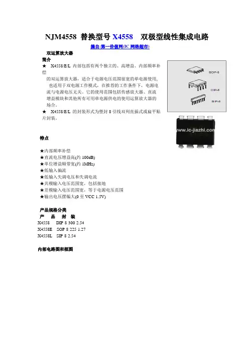
★X4558/E/L 的封装形式为塑封8引线双列直插式或扁平贴
片封装。
特点
★内部频率补偿
★直流电压增益高(约100dB)
★单位增益频带宽(约1MHz)
★低输入偏流
★低输入失调电压和失调电流
★共模输入电压范围宽,包括接地
★差模输入电压范围宽,等于电源电压范围
★输出电压摆幅大(0至VCC-1.5V)
产品规格分类
产品封装
X4558 DIP-8-300-2.54
X4558E SOP-8-225-1.27
X4558L SIP-8-2.54
内部电路图和框图
极限参数:
电参数(除非特别说明,Vcc=15.0V,VEE=-15.0,TA=25℃)
封装形式:。
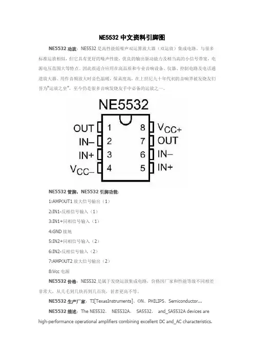
NE5532中文资料引脚图NE5532功放:NE5532是高性能低噪声双运算放大器(双运放)集成电路。
与很多标准运放相似,但它具有更好的噪声性能,优良的输出驱动能力及相当高的小信号带宽,电源电压范围大等特点。
因此很适合应用在高品质和专业音响设备、仪器、控制电路及电话通道放大器。
用作音频放大时音色温暖,保真度高,在上世纪九十年代初的音响界被发烧友们誉为“运放之皇”,至今仍是很多音响发烧友手中必备的运放之一。
NE5532管脚,NE5532引脚功能:1:AMPOUT1放大信号输出(1)2:IN1-反相信号输入(1)3:IN1+同相信号输入(1)4:GND接地5:IN2+同相信号输入(2)6:IN2-反相信号输入(2)7:AMPOUT2放大信号输出(2)8:Vcc电源NE5532价格:NE5532是属于发烧运放集成电路,价格因厂家和性能等级不同相差非常大,从几毛到几块再到几百块,甚者更高不等。
NE5532生产厂家:TI[TexasInstruments]、ON、PHILIPS、Semiconductor...NE5532描述:The NE5532,NE5532A,SA5532,and_SA5532A devices are high-performance operational amplifiers combining excellent DC and_AC characteristics.They feature very low noise,high output-drive capability,high unity-gainand_maximum-output-swing bandwidths,low distortion,high slew rate,input-protection diodes,and_output short-circuit protection. These operational amplifiers are compensated internally for unity-gain operation. These devices have specified maximum limits for equivalent input noise voltage.NE5532特性:Equivalent Input Noise Voltage:5 nV/√Hz Typ at 1 kHzUnity-Gain Bandwidth: 10 MHz TypCommon-Mode Rejection Ratio: 100 dB TypHigh DC Voltage Gain: 100 V/mV TypPeak-to-Peak Output Voltage Swing 26 V Typ With VCC± = ±15 V and_RL = 600 ?High Slew Rate: 9 V/μs TypNE5532相关型号:NE5532p、NE5532、NE5532A、SA5532、SA5532、ARC4558、JRC4558D、NE4558、OP275、EL2244、AD827你是不是在找?1、NE5532前置放大电路图2、NE5532前置3、NE5532放大4、NE5532电路5、NE5532芯片怎么用6、NE5532前级电路图7、NE5532负反馈电容8、5532运放2604哪个好9、NE5532p10、NE5532p用什么代换11、NE5532封装12、NE5532前级电路图经典13、opa2604运放比5532好吗NE5532相关运放:1、LM833N BJT工艺双运放噪声4.5nV/√Hz GBW:15M 压摆率:7V/uS 输入失调电压:0.3mV 温漂:2.0uV/℃2、OPA627 BJT工艺单运放噪声4.5nV/√Hz GBW:16M 压摆率:55V/uS 输入失调电压:0.13mV 温漂:1.2uV/℃3、OPA2604 FET工艺双运放噪声10nV//√Hz GBW:20M 压摆率:25V/uS 输入失调电压:1mV 温漂:8uV/℃4、NE5534 BJT工艺单运放噪声3.5nV/√Hz GBW:10M 压摆率:13V/uS 输入失调电压:0.5mV 温漂:规格书未给出5、NE5532 BJT工艺双运放噪声5nV/√Hz GBW:10M 压摆率:9V/uS 输入失调电压:0.5mV 温漂:规格书未给出代替NE5532,NE5532用什么代替?NE5532是双路低噪声高速音频运算放大器,op275:和5532比,胆性还重一点,解析力、低频、音场更好一点,可以买贴片的来打磨声卡用(特别是创新的),可以改善硬冷的数码声。
JRC设备型号NCU-245A-MR4说明书一、组合电台的交直流电源转换组合电台有三路电源输入:1、主配电板交流电2、应急发电机交流电3、GMDSS专用电平组合电台电源转换工作如下:主配电板交流电断掉,电台自动切换到应急发电机交流电,当主配电板和应急发电机交流电全部断掉时,电台切换到电平工作,C站和DSC进展重启,SSB需人工启动。
注意:不能对MF/HF电源和C站电源单独进展电源转换。
二、MF/HFa.DSCTEST以台6M为例1、在DSC单元上,按MENU进入菜单2、选择第11项TESTCALL3、在ADDRESS项输入ID:0041221004、按CALL键,呼叫,此时MF/HF自动转到DSC模式发射5、等待台回复,假如5分钟无回复,如此再次测试,或者更换频率在测试b.SSBTEST以台1211频段为例:1、在RADIOTELEPHONE单元上,按MODE/CLR键,转换到TEL模式2、按CH键,输入频道1211,按ENT确认3、按ANTTUNE键进展调谐4、调节RFGAIN与VOLUME将信号和声音调制最优5、拿起话筒,按住PTT与台通话,询问我方信号质量如何6、完毕通话三.INMARSAT-Ca。
LOGIN/LOGOUT1、按住ALT+U键,调出SETUP菜单2、选择LOG-ININITIATION或者LOG-OUTINITIATION入网或退出b。
CHOSEOCEANANDCHECKSIGNAL1、在屏幕界面,按左右方向键,选择NCS/LES-INFO菜单2、选择PREFERREDOCEANREGION进入洋区选择界面3、选择适宜的洋区,入网c、PRINTERSETUP1、按ALT+U,进入SETUP菜单2、选择PERIPHERALFUNCTION项,进入功能设置菜单3、在AUTOMATICMESSAGEPRINTOUT项,可选择打开或关闭自动打印d。
CHECKID检查本机ID1、按ALT+S进入STATUS选项2、选择MESSTATUS,可查看本机ID等信息e。
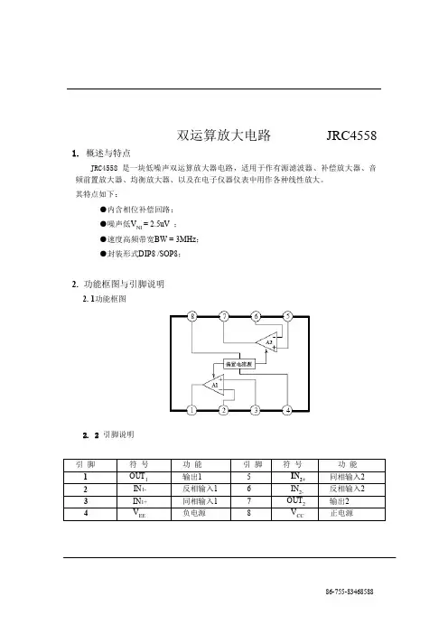
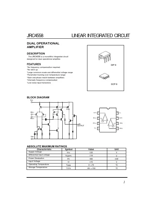
双运算放大电路JRC4558 1. 概述与特点
JRC4558 是一块低噪声双运算放大器电路,适用于作有源滤波器、补偿放大器、音频前置放大器、均衡放大器、以及在电子仪器仪表中用作各种线性放大。
其特点如下:
●内含相位补偿回路;
= 2.5uV ;
●噪声低V
NI
●速度高频带宽BW = 3MHz;
●封装形式DIP8 /SOP8;
2. 功能框图与引脚说明
2. 1功能框图
2. 2 引脚说明
3. 电特性
3. 1 极限参数
除非另有规定, T amb= 25℃
3. 2 电特性
除非另有规定T
amb = 25℃, V
CC
= +15V , V
EE
= -15V
4. 测试线路
左图开关位置如下
V OM:
S1=BS2断开S3断开情况下的输出电压
S1=AS2断开S3断开情况下的输出电压
S1=BS2接通S3断开情况下的输出电压
S1=AS2断开S3接通情况下的输出电压
Ios,Iosink::
S1=AS2断开S3接通情况下的输入电流
S1=BS2断开S3接通情况下的输出电流
A
VD
=20log(Vo/V)
BW是Vo=V
I 时的V
I
频率(MHz)
C1:隔直流电容
C2:高频旁路电容,云母或钛箔电容5. 特性曲线
6. 应用线路
7. 外形尺寸7. 1 DIP8封装
7. 2 SOP8封装。
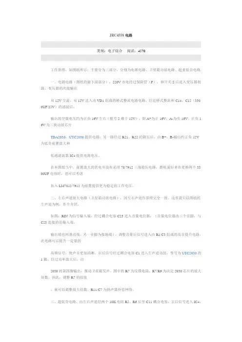
JRC4558电路类别:电子综合阅读:4570工作原理,如图纸所示:主要分为三部分。
分别为电源电路、卫星箱功放电路、超重低音电路.一、电源电路(图纸的最下面部分):220V市电经过保险管(F),和开关S后进入变压器初级,变压器的次级输出双12V交流,双12V送入由VD1组成的桥式整流电路电路,经过桥式整流和C14,C15(330 0UF/25V)的滤波后,输出的空载电压约为正负16V左右(根号2乘于12V),即A+为正16V,A-为负16V。
正负1 6V为三块功放芯片TDA2030,UTC2030提供电源。
另一路经过R21、R22的降压后,由B+,B-输出约正负12V 为低音前置放大和低通滤波器IC4提供电源电压。
在本图纸当中,前置放大的供电并没有采用78/7912三端稳压电路,磨机爱好者在更换两个33 00UF电容时,也可以考虑加入LM7812/7912为前置提供更为稳定的工作电压。
二、左右声道放大电路(卫星箱功放电路),因左右声道作原理完全一致。
这里我只以图纸的左声道为例,作个介绍。
如图:RIN为信号输入端,经过耦合电容C23进入音量电位器,(音量电位器由三个引脚,与C23连接的是输入端,输出端也叫滑动端、另一引脚为接地端),调整音量后信号进入由R1/C3组成的高音提升电路,此电路可以提升一定量的高频信号,使声音更加清晰。
尔后信号经过耦合电容C1进入左声道功放,型号为UTC2030的1脚,经过功率放大后,由2030的第四脚输出,推动卫星箱发声。
图中的R7为反馈电阻,R7/R9为决定2030芯片的放大倍数。
因此,调整R7的阻值,就可以调整放大倍数。
R11/C7为扬声器补偿网络。
三、超低音电路。
由左右声道经两个10K电阻R5、R6后至C11耦合电容,尔后信号进入IC4,型号为JRC4558的3脚,图中IC4A为超低音的前置放大器。
R201T将此放大器的放大倍数设置为6倍左右。
(R17/R18),经过前置放大后,才能保证足够大的驱动电压,获得足够大的音量。
Zoom® ComStar TM 56KSpeakerPhone/FaxModemA Complete CommunicationsCenter For Your Computer!The Zoom ComStar 56K Model 2818 for PC-compatible computers combines a full-featured V.34modem capable of 56,000 Kbps Internet and centralsite downloads with a powerful voice mail system,digital answering machine, 14,400 bps fax, convenientspeed dialer, and a synchronous interface supportingthe ITU H.324 videophone technology standard. It isPlug and Play compatible for easy installation underMicrosoft® Windows® 95 and is also softwareconfigurable.The Zoom ComStar 56K comes complete with a high-quality external microphone and speaker. It comeswith Cheyenne® BitWare® Fax/Voice/Data forWindows; ZOOM/LINK® CD-ROM with modem-enabled games, conferencing software, supportinformation, and more.About the Zoom ComStar 56KZoom ComStar 56K Speakerphone/FaxModem transforms your ordinary computer into anextraordinary telecommunications tool. ComStar 56K (internal) Model 2818 for PC-compatible computers is a high-speed V.34 faxmodem that can download data from compatible sites atspeeds up to 56,000 bps and at higher speeds with compression for fast Internet and LAN access.It combines a full-featured K56flex TM faxmodem, 14,400 bps fax, and full-duplex speakerphone over conventional telephone lines and features flash memory and reprogrammable DSP fordownloading feature enhancements and upgrades to future standards with simple softwarecommands. Other advanced features include a synchronous interface supporting the ITU H.324 videophone technology standard,* digital answering machine, voice mail, convenient speeddialer, and Plug-and-Play compatibility for easy installation. The Zoom ComStar 56K comescomplete with a high-quality external microphone and speaker, and all necessary software. ComStar 56K is built in the U.S.A. by Zoom Telephonics, Inc., a leading supplier of telecommunications equipment since 1977 and is backed by Zoom's outstanding 7-year warranty. Featuresr K56flex technology for 56,000 bps data downloads from compatible sitesr33,600 bps V.34 data transmission speedr14,400 bps Group 3, Class 1 and 2 faxr V.42bis and MNP 5 compression for data speeds up to 230,400 bpsr Reprogrammable Digital Signal Processor (DSP) enables easy software upgradeability to assure superior interoperability and overall performance and easy upgrades to futurestandards.r Flash memory for easy firmware upgradesr56K Faxmodem: Connect to the Internet, World Wide Web and on-line services, anddownload files fast and error-free at up to 56,000 bps with K56flex, the joint development of Rockwell and Lucent Technologies. Send "printer-quality" faxes direct from your PC, plus faxback and fax-on-demand.r Speakerphone: For "hands-free" communications and conference calls. True full-duplex speakerphone lets callers on both ends talk at the same time for natural conversation.r Videophone-Ready: Supports the ITU H.324 video technology standard and H.324compliant software from Intel, PictureTel, VDONet, Smith Micro, and others.*r Digital Answering Machine: An easy-to-use personal answering machine with high-quality recording and playback, pager notification, and other advanced features.r Voice Mail: A full-featured, configurable voice mail system for home or office withmultiple mailboxes, fax-on-demand, and remote retrieval of messages.r Other Features: Plug-and-Play with Windows 95 computers (software configurable also), VoiceView® compatibility, Directory Dialing, Distinctive Ring,** Caller ID,** andZoomGuard lightning protection.Technical SpecificationsData Speeds:r300 to 33,600 bps full-duplex with international standardsr Up to 56,000 bps receive/33,600 bps send with K56flexFax Speeds:r 300 to 14,400 bpsr Group 3, Class 1 and Class 2Standards Supported:r Data: K56flex, V34, V.32bis, V.32, V.22bis, V.22 A/B, V.22, V.23, V.21, Bell 103/212Ar Fax: V.33, V.29, V.17, V.27ter, V.21 channel 2Compression: V.42bis, MNP 5r Error Control: V.42, MNP 2 - 4, MNP 10 and MNP 10ECr Plug and Playr AT and extended AT command set compatibleCommand Set:Hayes AT-Command compatible, with extended MNP 5, MNP 10, and V.42bis commandsVoice Encoding:Enhanced ADPCM, programmable at 2 or 4 bits per sampleSpeakerphone:Full-duplex with microphone and speaker included; headset capability; software volume controlInterface:Plug and Play; COM1 - COM8, IRQ, 3, 4, 5, 7, 9, 10, 12, 15 supports TAPIVideoconferencing enabled:Synchronous interface supports ITU H.324 standard for videoconferencing applications.*Hardware Features:r Dual RJ-11 telephone jacks one for phone line, one for optional phoner Output jack for external 8 ohm audio speaker (8 ohm external speaker included)r Input jack for external microphone (microphone included)r Jumper-selectable electret microphone biasr Telephone cable with RJ-11 connectorsr Buffered 16550 UART to reduce PC interrupts and boost performancer Handset record and playbackDimensions and Power Requirements:r Dimensions: standard IBM PC board 2.7 in. W by 5.4 in. L by 0.75 in. H (fits 16-bit PC-compatible slot)r Power consumption: 1.5W typicalSystem Requirements:r486 or faster PC compatible computer with 1 available 16-bit ISA slotr8 MB RAMr 3.5 in. floppy driver Hard drive with a minimum of 5 MB available r Microsoft Windows 3.1 or higherr Mouse recommendedRegulatory Approvals:rFCC Parts 15B and 68 r UL, C-ULr Industry CanadaWarranty:Warranted against defects in material andworkmanship for a period of seven years from the date of original retail purchase* Requires video camera and video capture support, sound card with microphone input, ITU H.324-compliant videoconferencing application, and appropriate computer and operating system to run the application.** Requires Distinctive Ring or Caller ID support from local telephone company.Zoom Telephonics, Inc.207 South Street Boston, MA 02111617 423-1072800 631-3116Fax: 617 423-3923Web Site: BBS: 617 423-3733Nasdaq: ZOOMZoom is a registered trademark and ComStar, Zoom/FaxModem, ZoomGuard are trademarks of Zoom Telephonics, Inc. K56flex is a trademark of Rockwell International Corporation and Lucent Technologies, Inc. Windows is a registered trademark of Microsoft. MNP is a registered trademark and MNP 10EC is a trademark of Microcom Inc. All other registered trademarks and trademarks are the property of their respective owners.Made in the U.S.A.©2000 Zoom Telephonics, Inc.1777。
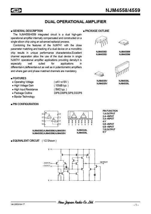
NJM4558D,NJM4558M,NJM4558V NJM4559D,NJM4559M,NJM4559V NJM4558L NJM4559L PIN FUNCTION 1.A OUTPUT2.A –INPUT3.A +INPUT4.V -5.B +INPUT6.B –INPUT7.B OUTPUT 8.V + DUAL OPERA TIONAL AMPLIFIER■ GENERAL DESCRIPTION ■ PACKAGE OUTLINE The NJM4558/4559 integrated circuit is a dual high-gain operational amplifier internally compensated and constructed on a single silicon chip using an advanced epitaxial process. Combining the features of the NJM741 with the close parameter matching and tracking of a dual device on a monolithicchip results in unique performance characteristics.Excellentchannel separation allow the use of the dual device in single NJM741 operational amplifier applications providing density .It is especially well suited for applications indifferential-in,defferential-out as well as in potentiometric amplifiers and where gain and phase matched channels are mandatory .■ FEA TURES● Operating Voltage ( ±4V~±18V )● High Voltage Gain ( 100dB typ. ) ● High Input Resistance ( 5M Ω typ. ) ● Package Outline DIP8,DMP8,SIP8,SSOP8 ● Bipolar T echnology■ PIN CONFIGURA TION■ EQUIVALENT CIRCUIT ( 1/2 Shown ) NJM4558LNJM4559LNJM4558D NJM4559D NJM4558M NJM4559MNJM4558V NJM4559V■ ABSOLUTE MAXIMUM RA TINGS( T a=25˚C )UNITPARAMETER SYMBOL RATINGS18 VSupply Voltage V+/V- ±30 VDifferential Input Voltage V ID ±Input Voltage V IC± 15 ( note ) V( DIP8 ) 500( DMP8 ) 300mWPower Dissipation P D( SSOP8 ) 250( SIP8 ) 800Operating T emperature Range T opr -40~+85 ˚CStorage T emperature Range T stg -40~+125 ˚C( note ) For supply voltage less than ±15V,the absolute maximum input voltage is equal to the supply voltage.■ ELECTRICAL CHARACTERISTICS( V+/V-=±15V,T a=25˚C )MAX.UNITTYP.MIN.CONDITIONPARAMETER SYMBOL TESTInput Offset Voltage V IO R S≤10kΩ- 0.5 6 mVInput Offset Current I IO- 5 200 nAInput Bias Current I B- 25 500 nAInput Resistance R IN0.3 5 - MΩLarge Signal Voltage Gain A V R L≥2kΩ,V O=±10V 86 100 - dBMaximum Output Voltage Swing 1 V OM1R L≥10kΩ± 12 ± 14 - VMaximum Output Voltage Swing 2 V OM2R L≥2kΩ± 10 ± 13 - V12 14 - VInput Common Mode Voltage Range V ICM±Common Mode Rejection Ratio CMR R S≤10kΩ70 90 - dBSupply Voltage Rejection Ratio SVR R S≤10kΩ76.5 90 - dBOperating Current I CC- 3.5 5.7 mASlewRateV/µs- NJM4558 SR -1V/µs-2NJM4559 SR -Equivalent Input Noise Voltage V NI RIAA,R S=2.2kΩ,30kHz LPF - 1.4 - µVrmsGain Bandwidth Product GBMHz NJM4558 3MHz NJM4559 6。

布瑞特单圈绝对值旋转编码器RS485产品说明书深圳布瑞特科技有限公司ShenZhen Briter Technology Co.Ltd产品优势特性●RS485数字通讯信号输出,数字输出信号既有多圈值、单圈绝对值;●采用标准的ModBus-RTU通讯规约,支持组态王、Intouch、FIX、synall 等流行软件,能与AB、西门子、施耐德、GE等国际著名品牌的设备及系统之间实现数据通信;●单圈编码器在不掉电情况下可作电子多圈编码器使用(此功能非断电记忆),最高可达百万圈;增加返回速度功能,便于使用者计算;●单圈量程范围内任何位置都是唯一的,即使有干扰或断电运动,都不会丢失位置信息;●单圈分辨率有1024(10bit)、4096(12bit)、16384(14bit)、32768(15 bit),量程范围内最高可实现0.01度的分辨率;●所有参数均可通过电脑的RS485通讯进行设定,可在任意位置设定零点,因此安装编码器时可将设备停留任意位置,无需考虑本编码器的旋转位置、即可固定好连接轴,通电后只要在外部引线处或通过RS485通讯进行一次置零操作即可自动修正;●特别适用于塔式起重机、矿山起重机、施工升降机、机床、3D打印机、自动化流水线、工业机器人、印刷机械、包装机械、物流机械、移动广告屏幕滑轨等设备的高度、行程、角度及速度的可靠/精确测量。
产品型号说明型号:RS485接口--3D 模型以及相关资料请到布瑞特科技官网下载。
尺寸型号图1:输出6mm IP54尺寸型号图2:输出轴8mm IP54机械尺寸线出口方向与3个M3安装孔的角度关系是随机的D 字型轴尺寸比例5:1螺纹孔深6mm尺寸型号图3:盲孔8mm IP54尺寸型号图4:输出6mm IP67尺寸型号图5:输出8mm IP67注意事项●编码器属于精密仪器,请轻拿轻放、小心使用,尤其对编码器轴请勿敲、撞击及硬拽等。
●编码器与机械连接应选用柔性连接器或弹性支架,应避免刚性联接不同心造成的硬性损坏。
POST OFFICE BOX 655303 • DALLAS, TEXAS 75265V IO Input offset voltage V O = 0V O = 0V O = 0mV nA nAI IO Input offset current I IB Input bias currentV IInput voltage range V/mVRC4559DUAL HIGH-PERFORMANCE OPERATIONAL AMPLIFIERPOST OFFICE BOX 655303 •DALLAS, TEXAS 75265元器件交易网元器件交易网IMPORTANT NOTICETexas Instruments and its subsidiaries (TI) reserve the right to make changes to their products or to discontinueany product or service without notice, and advise customers to obtain the latest version of relevant informationto verify, before placing orders, that information being relied on is current and complete. All products are soldsubject to the terms and conditions of sale supplied at the time of order acknowledgement, including thosepertaining to warranty, patent infringement, and limitation of liability.TI warrants performance of its semiconductor products to the specifications applicable at the time of sale inaccordance with TI’s standard warranty. Testing and other quality control techniques are utilized to the extentTI deems necessary to support this warranty. Specific testing of all parameters of each device is not necessarilyperformed, except those mandated by government requirements.CERTAIN APPLICATIONS USING SEMICONDUCTOR PRODUCTS MAY INVOLVE POTENTIAL RISKS OFDEATH, PERSONAL INJURY, OR SEVERE PROPERTY OR ENVIRONMENTAL DAMAGE (“CRITICALAPPLICATIONS”). TI SEMICONDUCTOR PRODUCTS ARE NOT DESIGNED, AUTHORIZED, ORWARRANTED TO BE SUITABLE FOR USE IN LIFE-SUPPORT DEVICES OR SYSTEMS OR OTHERCRITICAL APPLICATIONS. INCLUSION OF TI PRODUCTS IN SUCH APPLICATIONS IS UNDERSTOOD TOBE FULLY AT THE CUSTOMER’S RISK.In order to minimize risks associated with the customer’s applications, adequate design and operatingsafeguards must be provided by the customer to minimize inherent or procedural hazards.TI assumes no liability for applications assistance or customer product design. TI does not warrant or representthat any license, either express or implied, is granted under any patent right, copyright, mask work right, or otherintellectual property right of TI covering or relating to any combination, machine, or process in which suchsemiconductor products or services might be or are used. TI’s publication of information regarding any thirdparty’s products or services does not constitute TI’s approval, warranty or endorsement thereof.Copyright © 1998, Texas Instruments Incorporated。
UTC4558 替换型号X4558双极型线性集成电路
摘自:第一价值网(IC网络超市)
双运算放大器
简介
★X4558/E/L 内部包括有两个独立的、高增益、内部频率补
偿的双运算放大器,适合于电源电压范围很宽的单电源使用,
也适用于双电源工作模式,在推荐的工作条件下,电源电
流与电源电压无关。
它的使用范围包括传感放大器、直流
增益模块和其他所有可用单电源供电的使用运算放大器的
场合。
★X4558/E/L 的封装形式为塑封8引线双列直插式或扁平贴
片封装。
特点
★内部频率补偿
★直流电压增益高(约100dB)
★单位增益频带宽(约1MHz)
★低输入偏流
★低输入失调电压和失调电流
★共模输入电压范围宽,包括接地
★差模输入电压范围宽,等于电源电压范围
★输出电压摆幅大(0至VCC-1.5V)
产品封装
X4558 DIP-8-300-2.54
X4558E SOP-8-225-1.27
X4558L SIP-8-2.54
内部电路图和框图
极限参数:
电参数(除非特别说明,Vcc=15.0V,VEE=-15.0,TA=25℃)
封装形式:。
5804中⽂资料Combining low-power CMOS logic with high-current and high-voltage bipolar outputs, the UCN5804B and UCN5804LB BiMOS II translator/drivers provide complete control and drive for a four-phase unipolar stepper-motor with continuous output current ratings to 1.25 A per phase (1.5 A startup) and 35 V.The CMOS logic section provides the sequencing logic, DIRECTION and OUTPUT ENABLE control, and a power-on reset function. Three stepper-motor drive formats, wave-drive (one-phase), two-phase, and half-step are externally selectable. The inputs are compatible with standard CMOS, PMOS, and NMOS circuits. TTL or LSTTL may require the use of appropriate pull-up resistors to ensure a proper input-logic high.The wave-drive format consists of energizing one motor phase at a time in an A-B-C-D (or D-C-B-A) sequence. This excitation mode consumes the least power and assures positional accuracy regardless of any winding inbalance in the motor. Two-phase drive energizes two adjacent phases in each detent position (AB-BC-CD-DA). This sequence mode offers animproved torque-speed product, greater detent torque, and is less susceptible to motor resonance. Half-step excitation alternates between the one-phase and two-phase modes (A-AB-B-BC-C-CD-D-DA), providing an eight-step sequence.The bipolar outputs are capable of sinking up to 1.5 A and withstanding 50 V in the off state (sustaining voltages up to 35 V). Ground-clamp and flyback diodes provide protection against inductive transients. Thermal protection circuitry disables the outputs when the chip temperature is exces-sive.Both devices are rated for operation over the temperature range of -20°C to +85°C. The UCN5804B is supplied in a 16-pin dual in-line plastic batwing package with a copper lead frame and heat-sinkable tabs for improved power dissipation capabilities; the UCN5804LB is supplied in a 16-lead plastic SOIC batwing package with a copper lead frame and heat-sinkable tabs.FEATURESI 1.5 A Maximum Output Current I 35 V Output Sustaining VoltageI Wave-Drive, Two-Phase, and Half-Step Drive Formats I Internal Clamp DiodesI Output Enable and Direction Control I Power-On ResetI Internal Thermal Shutdown CircuitryBiMOS II UNIPOLARSTEPPER-MOTOR TRANSLATOR/DRIVERAlways order by complete part number, e.g., UCN5804B .Data Sheet 26184.12C*5804115 Northeast Cutoff, Box 15036Worcester, Massachusetts 01615-0036 (508) 853-********BiMOS II UNIPOLAR STEPPER-MOTORTRANSLATOR/DRIVERTRUTH TABLEDrive Format Pin 9Pin 10Two-Phase L L One-Phase H L Half-Step L H Step-InhibitHHTYPICAL INPUT CIRCUITDwg. EP-021-4TYPICAL OUTPUT DRIVERDwg. EP-010-5INCopyright ? 1987, 2000 Allegro MicroSystems, Inc.5075100125150510A L L O W A B L E P A C K A G E P O W E R D I S S I P A T I O N I N W A T T STEMPERATURE IN °C43225Dwg. GP-049-2A5804BiMOS II UNIPOLAR STEPPER-MOTOR TRANSLATOR/DRIVER/doc/a3712eddb9f3f90f76c61b7c.htmlELECTRICAL CHARACTERISTICS at T A = 25°C, T J ≤ 150°C, V DD = 4.5 V to 5.5 V (unless otherwise noted). Limits CharacteristicSymbol Test Conditions Min.Typ.Max.Units Output Leakage Current I CEX V OUT = 50 V—1050µA Output Sustaining Voltage V CE(sus)I OUT = 1.25 A, L = 3 mH 35——V Output Saturation VoltageV CE(SAT)I OUT = 700 mA — 1.0 1.2V I OUT = 1 A — 1.1 1.4V I OUT= 1.25 A— 1.2 1.5V Clamp Diode Leakage Current I R V R = 50 V —1050µA Clamp Diode Forward Voltage V F I F = 1.25 A — 1.53.0V Input CurrentI IN(1)V IN = V DD —0.5 5.0µA I IN(0)V IN = 0.8 V —-0.5-5.0µA Input VoltageV IN(1)V DD = 5 V3.5— 5.3V V IN(0)-0.3—0.8V Supply Current I DD 2 Outputs ON—2030mA Turn-Off Delay t ON 50% Step Inputs to 50% Output ——10µs Turn-On Delayt OFF 50% Step Inputs to 50% Output ——10µs Thermal Shutdown TemperatureT J—165—°CTIMING CONDITIONSA. Minimum Data Set Up Time . . . . . . . . . . . . . . . . . . . . . . . . 100 nsB. Minimum Data Hold Time . . . . . . . . . . . . . . . . . . . . . . . . . . 100 nsC. Minimum Step Input Pulse Width . . . . . . . . . . . . . . . . . . . . . 3.0 µsDwg. W-110AONE PHASE HALF STEPOOUTPUT ENABLEOUTPUT C OUTPUT DCLOCK115 Northeast Cutoff, Box 15036Worcester, Massachusetts 01615-0036 (508) 853-50005804BiMOS II UNIPOLAR STEPPER-MOTORTRANSLATOR/DRIVERWAVE-DRIVE SEQUENCEHalf Step = L, One Phase = H Step A B C D POR ON OFF OFF OFF 1ON OFF OFF OFF 2OFF ON OFF OFF 3OFF OFF ON OFF 4OFFOFFOFFONTWO-PHASE DRIVE SEQUENCEHalf Step = L, One Phase = LStep A B C D POR ON OFF OFF ON 1ON OFF OFF ON 2ON ON OFF OFF 3OFF ON ON OFF 4OFFOFFONONHALF-STEP DRIVE SEQUENCEHalf Step = H, One Phase = LStep A B C D POR ON OFF OFF OFF 1ON OFF OFF OFF 2ON ON OFF OFF 3OFF ON OFF OFF 4OFF ON ON OFF 5OFF OFF ON OFF 6OFF OFF ON ON 7OFF OFF OFF ON 8ONOFFOFFONAPPLICATIONS INFORMATIONInternal power-on reset (POR) circuitry resets OUTPUT A (and OUTPUT D in the two-phase drive format) to the on state with initial applica-tion of the logic supply voltage. After reset, the circuit then steps according to the tables.The outputs will advance one sequenceposition on the high-to-low transition of the STEP INPUT pulse. Logic levels on the HALF-STEP and ONE-PHASE inputs will determine the drive format (one-phase, two-phase, or half-step). The DIRECTION pin determines the rotation se-quence of the outputs. Note that the STEP INPUT must be in the low state when changing the state of ONE-PHASE, HALF-STEP, or DIRECTION to prevent erroneous stepping.All outputs are disabled (off) when OUTPUT ENABLE is at a logic high. If the function is not required, OUTPUT ENABLE should be tied low.In that condition, all outputs depend only on the state of the step logic.During normal commutation of a unipolar stepper motor, mutual coupling between the motor windings can force the outputs of the UCN5804B below ground. This condition will cause forward biasing of the collector-to-substrate junction and source current from the output. For many L/R applications, this substrate current is high enough to adversely affect the logic circuitry and cause misstepping. External series diodes (Schottky are recommended for increasedefficiency at low-voltage operation) will prevent substrate current from being sourced through the outputs. Alternatively, external ground clamp diodes will provide a preferred current path from ground when the outputs are pulled below ground.Internal thermal protection circuitry disables all outputs when the junction temperature reaches approximately 165°C. The outputs are enabled again when the junction cools down to approxi-mately 145°C.5804BiMOS II UNIPOLAR STEPPER-MOTOR TRANSLATOR/DRIVER/doc/a3712eddb9f3f90f76c61b7c.htmlTYPICAL APPLICATION L/R Stepper-Motor DriveThe products described here are manufactured under one or more U.S. patents or U.S. patents pending.Allegro MicroSystems, Inc. reserves the right to make, from time to time, such departures from the detail specifications as may berequired to permit improvements in the performance, reliability, or manufacturability of its products. Before placing an order, the user is cautioned to verify that the information being relied upon is current.Allegro products are not authorized for use as critical components in life-support devices or systems without express written approval.The information included herein is believed to be accurate and reliable. However, Allegro MicroSystems, Inc. assumes no responsi-bility for its use; nor for any infringement of patents or other rights of third parties which may result from its use.115 Northeast Cutoff, Box 15036Worcester, Massachusetts 01615-0036 (508) 853-50005804BiMOS II UNIPOLAR STEPPER-MOTORTRANSLATOR/DRIVERUCN5804BDimensions in Inches (controlling dimensions)Dimensions in Millimeters(for reference only)NOTES:1.Exact body and lead configuration at vendor’s option within limits shown.2.Lead spacing tolerance is non-cumulative.3.Lead thickness is measured at seating plane or below.4.Webbed lead frame. Leads 4, 5, 12, and 13 are internally one piece.5.Supplied in standard sticks/tubes of 25 devices.Dwg. MA-001-17A in18Dwg. MA-001-17A mm185804 BiMOS II UNIPOLAR STEPPER-MOTOR TRANSLATOR/DRIVER/doc/a3712eddb9f3f90f76c61b7c.htmlUCN5804LB(add “TR” to part number for tape and reel) Dimensions in Inches(for reference only)Dimensions in Millimeters(controlling dimensions)NOTES:1.Exact body and lead configuration at vendor’s option within limits shown.2.Lead spacing tolerance is non-cumulative.3.Lead thickness is measured at seating plane or below.4.Webbed lead frame. Leads 4, 5, 12, and 13 are internally one piece.5.Supplied in standard sticks/tubes of 47 devices or add “TR” to part number for tape and reel.115 Northeast Cutoff, Box 15036Worcester, Massachusetts 01615-0036 (508) 853-50005804BiMOS II UNIPOLAR STEPPER-MOTORTRANSLATOR/DRIVERMOTOR DRIVERSFunctionOutput Ratings*Part Number ?INTEGRATED CIRCUITS FOR BRUSHLESS DC MOTORS3-Phase Power MOSFET Controller —28 V 39333-Phase Power MOSFET Controller —50 V 39323-Phase Power MOSFET Controller —50 V 76002-Phase Hall-Effect Sensor/Driver 400 mA 26 V 3626Bidirectional 3-Phase Back-EMFController/Driver ±600 mA 14 V 89062-Phase Hall-Effect Sensor/Driver 900 mA 14 V 36253-Phase Back-EMFController/Driver ±900 mA 14 V 8902–A 3-Phase Controller/Drivers ±2.0 A 45 V 2936 & 2936-120INTEGRATED BRIDGE DRIVERS FOR DC AND BIPOLAR STEPPER MOTORSDual Full Bridge with Protection & Diagnostics ±500 mA 30 V 3976PWM Current-Controlled Dual Full Bridge ±650 mA 30 V 3966PWM Current-Controlled Dual Full Bridge ±650 mA 30 V 3968PWM Current-Controlled Dual Full Bridge ±750 mA 45 V 2916PWM Current-Controlled Dual Full Bridge ±750 mA 45 V 2919PWM Current-Controlled Dual Full Bridge ±750 mA 45 V 6219PWM Current-Controlled Dual Full Bridge ±800 mA 33 V 3964PWM Current-Controlled Full Bridge ±1.3 A 50 V3953PWM Current-Controlled Dual Full Bridge ±1.5 A 45 V 2917PWM Current-Controlled Microstepping Full Bridge ±1.5 A 50 V 3955PWM Current-Controlled Microstepping Full Bridge ±1.5 A 50 V 3957PWM Current-Controlled Dual DMOS Full Bridge ±1.5 A 50 V 3972Dual Full-Bridge Driver ±2.0 A 50 V 2998PWM Current-Controlled Full Bridge ±2.0 A 50 V3952DMOS Full Bridge PWM Driver ±2.0 A 50 V 3958Dual DMOS Full Bridge ±2.5 A 50 V 3971UNIPOLAR STEPPER MOTOR & OTHER DRIVERSVoice-Coil Motor Driver ±500 mA 6 V 8932–A Voice-Coil Motor Driver ±800 mA 16 V 8958Unipolar Stepper-Motor Quad Drivers 1 A 46 V 7024 & 7029Unipolar Microstepper-Motor Quad Driver 1.2 A 46 V 7042Unipolar Stepper-Motor Translator/Driver 1.25 A 50 V 5804Unipolar Stepper-Motor Quad Driver 1.8 A 50 V 2540Unipolar Stepper-Motor Quad Driver 1.8 A 50 V 2544Unipolar Stepper-Motor Quad Driver 3 A 46 V 7026Unipolar Microstepper-Motor Quad Driver 3 A 46 V 7044*Current is maximum specified test condition, voltage is maximum rating. See specification for sustaining voltage limits or over-current protection voltage limits. Negative current is defined as coming out of (sourcing) the output.?Complete part number includes additional characters to indicate operating temperature range and package style.Also, see 3175, 3177, 3235, and 3275 Hall-effect sensors for use with brushless dc motors.。