防焊制程讲解模板ppt
- 格式:ppt
- 大小:3.12 MB
- 文档页数:54


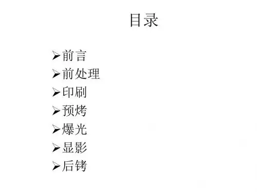
防焊制程流程(中英文实用版)英文文档内容:The solder mask process is a critical step in the printed circuit board (PCB) manufacturing industry.It involves applying a layer of protective material to the copper conductors on a PCB to prevent the solder from attaching to unwanted areas during the reflow soldering process.Here is an overview of the solder mask process flow:1.Design: The first step in the solder mask process is to design the solder mask layer using specialized software.This design is based on the Gerber files provided by the customer, which show the outlines of the PCB components and the desired solder mask color.2.Printing: Once the solder mask design is complete, it is sent to a printing machine.The machine uses a stencil to transfer the solder mask material (usually a photosensitive liquid or paste) onto the copper conductors of the PCB.The solder mask material is cured using UV light or heat, depending on the type of material used.3.Developing: After the solder mask material is cured, it is developed to remove the unexposed material, leaving behind a solid solder mask layer on the copper conductors.The developing process can be done manually or using an automated machine.4.Inspection: The PCB is then inspected for any defects in the soldermask layer, such as pinholes, missing solder mask, or misalignment.This inspection can be done using automated optical inspection (AOI) machines or manual inspection.5.Plating: The solder mask layer is then plated with a layer of protective material, such as epoxy or polyimide, to enhance the durability of the solder mask and to prevent any chemical damage during the subsequent PCB assembly processes.6.Drilling: After the plating process, the PCB is drilled to create holes for components and connectors.The drilling process is typically done using a CNC machine.7.Routining: The PCB is then routed to create the final outline of the board.The routing process is also done using a CNC machine.8.Finishing: The final step in the solder mask process is to remove any remaining solder mask material from the drill holes and to clean the PCB surface.This is done using a chemical etching process or a laser ablation process.The solder mask process is crucial to the functionality and reliability of the PCB, as it ensures that the solder attaches only to the desired areas on the board.中文文档内容:防焊制程是印刷电路板(PCB)制造行业中的关键步骤。