数字电路-第五章习题答案
- 格式:pdf
- 大小:150.16 KB
- 文档页数:9

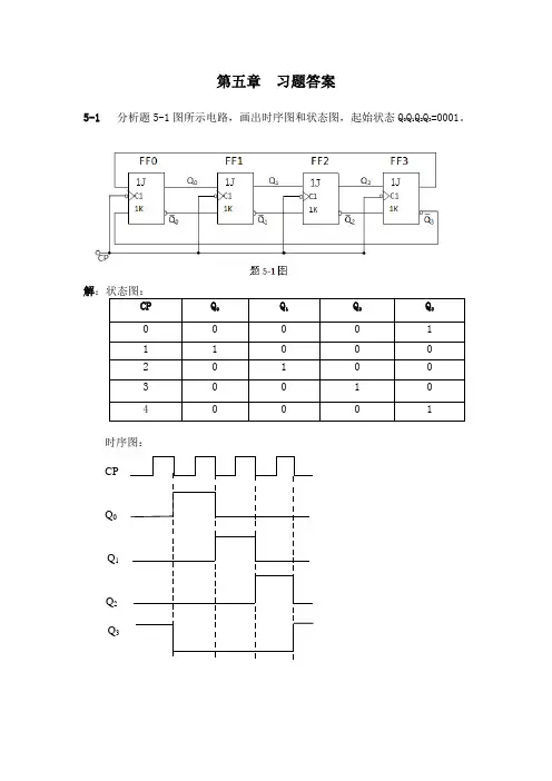
第五章习题答案5-1分析题5-1图所示电路,画出时序图和状态图,起始状态Q0Q1Q2Q3=0001。
解CP Q0 Q1Q2Q30 0 0 0 11 1 0 0 02 0 1 0 03 0 0 1 04 0 0 0 1 时序图:CPQ0Q1Q2Q35-2分析题5-2图所示电路,画出电路的状态图。
解CP Q0 Q1 Q20 0 0 01 1 0 02 0 1 03 0 0 14 0 0 05-3 JK触发器组成5-3图所示电路。
分析该电路为几进制计数器,并画出电路的状态图。
CP Q1 Q2Q30 0 0 01 1 0 02 0 1 03 1 1 04 0 0 15 0 0 0 该电路为五进制计数器5-4JK触发器促成如图5-4图所示的电路。
(1)分析该电路为几进制计数器,画出状态图。
(2)若令K3= 1,电路为几进制计数器,画出其状态图。
解:(1CP Q1 Q2Q30 1 2 3 4 5 6 7 0 0 01 0 00 1 01 1 00 0 11 0 1 0 1 1 0 0 0为7进制计数器CP Q1 Q2Q30 1 2 3 4 5 0 0 01 0 00 1 01 1 00 0 11 0 0为4进制计数器5-5 试画出题5-5图(a)所示电路中B,C端的波形。
输入端A,CP波形如题5-5图(b)所示,触发器的起始状态为零。
1 2 3 4 5 6 7 8 9 10 11 12 13 14 15 16 17 18 19CPAQ0Q1BC5-6分析题5-6图所示电路,画出电路的状态图,说明电路能否自启动。
CP Q1 Q2Q3Z0 1 2 3 4 5 6 7 0 1 0 0 0 01 0 1 0 1 1 1 00 1 1 11 0 0 0 1 1 0 00 1 0 01 0 1 00 0 1 01 0 0 0该电路能够自启动5-7 分析题5-7图所示电路,画出电路的状态图,说明电路能否自启动。
CP Q4 Q3Q2Q11234 567111111111 0 0 0 00 0 0 11 0 0 11 1 0 11 1 1 00 1 1 11 0 1 11 1 0 10 0 1 00 0 0 10 0 1 11 0 0 10 1 0 00 0 1 10 1 0 11 0 1 10 1 1 00 0 1 11 0 0 00 1 0 11 0 1 00 1 0 11 1 0 00 1 1 11 1 1 1 1 1 1 0由状态图可见,电路图能够自启动5-8画出题5-8图所示电路的状态图和时序图,简要说明电路的基本功能。

数字电路答案 第一章习题1-1 (1)10108222*86*8268201011026261011021616101100001011016(2) 211081081*85*84*81548200110010115415411011002166110110*********6CC(3)10110813.1251*85*81*815.18200100110115.115.11101.00121621101.0011101.0010.2DD(4)211108131.6252*80*83*85*8203.582010000011101203.5203.510000011.1012168310000011.10110000011.101083.AA1-2(1)285510110110110155 2162101101001011012DD10810555*85*845(2)2834511100101011100101345 216511100101111001015EE2108103453*84*85*8229(3)28514101.0011101.0011005.14 21653101.00110101.00115.30128105.145*81*84*85.1875(4)28744100111.101100111.10147.421627100111.10100100111.101027.AA101018625.398*58*78*45.47=++=-1-3 (1)10810161*86*8148200111016161110 21611101110EE(2)218101721*87*82*812282001010111172172111101016727101001111111010A A==(3)101281061.536*81*85*83*849.6728200111010101161.5361.53110001.101011 21631110001.10101100110001.1010110031.AC AC(4)21012810126.741*82*86*87*84*886.937582001010100110111126.74126.741010110.1111216561010110.111101010110.111156.FF1-4 (1)1620010101022101010A A28521010101010105210810525*82*842(2)16210110010111122101100101111B F B F2875451011001011111011001011115457321081054575*84*85*87*82863(3)1621101111000113.3.11010011.111D E D E28732311010011.111011010011.111323.72101810323.73*82*83*87*8211.875(4)162000111111100001110011 3.913.9111000011.11111001C F C F28770362111000011.11111001111000011.111110010703.762210123810703.7627*80*83*87*86*82*8451.97261-5(1)AC AB C B A +=+)(左式=右式,得证。
自我检查题5.1 时序电路和组合电路的根本区别是什么?同步时序电路与异步时序电路有何不同?解答:从功能上看,时序电路任何时刻的稳态输出不仅和该时刻的输入相关,而且还决定于该时刻电路的状态,从电路结构上讲,时序电路一定含有记忆和表示电路状态的存储器。
而组合电路任何时刻的稳态输出只决定于该时刻各个输入信号的取值,由常用门电路组成则是其电路结构的特点。
在同步时序电路中,各个触发器的时钟信号是相同的,都是输入CP 脉冲,异步时序电路则不同,其中有的触发器的时钟信号是输入cp 脉冲,有的则是其他触发器的输出,前者触发器的状态更新时同步的,后者触发器状态更新有先有后,是异步的。
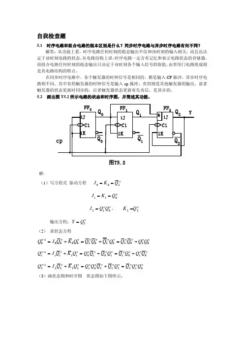
5.2 画出图T5.2所示电路的状态和时序图,并简述其功能。
图T5.2解:(1)写方程式 驱动方程 nQ K J 200==n Q K J 011==n n Q Q J 012=, n Q K 22=输出方程:nQ Y 2= (2) 求状态方程nn n n n n n n n n n Q Q Q Q Q Q Q Q Q K Q J Q 02020202000010+=+=+=+ n n n n n n n n n n n Q Q Q Q Q Q Q Q Q K Q J Q 01011010111111+=+=+=+ n n n n n n n n n n n Q Q Q Q Q Q Q Q Q K Q J Q 01222201222212=+=+=+(3)画状态图和时序图 状态图如下图所示:101时序图如下图所示:CP Q 0Q 1Q 25.3 试用边沿JK 触发器和门电路设计一个按自然态序进行计数的七进制同步加法计数器。
解:(1)状态图如下图:(2)求状态方程、输出方程CQ Q Q n n n /101112+++的卡诺图如下图所示:输出方程为nn Q Q C 12=状态方程:n n n n n Q Q Q Q Q 120112+=+ n n n n n n Q Q Q Q Q Q 0120111+=+ n n n n n Q Q Q Q Q 120110+=+驱动方程:n n n n n n n n n n n n n n n Q Q Q Q Q Q Q Q Q Q Q Q Q Q Q 0122120121220112)(++=++=+n n n n n n Q Q Q Q Q Q 1021011+=+n n n n n Q Q Q Q Q 0012101)(++=+与JK 触发器的特性方程 比较,可以得到驱动方程 n n Q Q J 012= 、 n Q K 12=n Q J 01= 、n n Q Q K 021=n n n n Q Q Q Q J 12120=+= 10=K(4) 无效状态转换情况 111/1000 能自启动(5) 逻辑图如下图所示:5.4 画出用时钟脉冲上升沿触发的边沿D 触发器组成的4位二进制异步加法计数器和减法计数器的逻辑电路图。
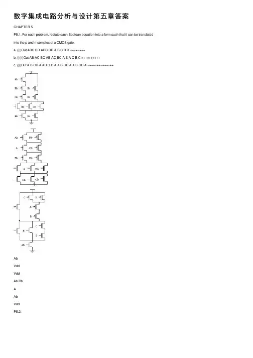
数字集成电路分析与设计第五章答案CHAPTER 5P5.1. For each problem, restate each Boolean equation into a form such that it can be translated into the p and n-complex of a CMOS gate.a. ()()Out ABC BD ABC BD A B C B D =+=+=+++b. ()()()Out AB AC BC AB AC BC A B A C B C =++=++=+++c. ()()Out A B CD A AB C D A A B CD A A B CD A =+++=++=+++=++AbVddVddAb BbAAbVddP5.2.AP5.3. First, convert the equation into its p and n-complex.()()()()()()()()()()()Out A B C BC AB AB C BC AB AB C BC AB AB C BC AB AB C BC AB AB C B C =⊕+=++=++=+=++=+++VddCbP5.4. The truth table is given below in terms of voltages. The function is F A B =The worse case V OH is V DD and the worse case V OL is 0V.P5.5. The first circuit is a NOR gate while the second is a NAND gate. The V OL and V OHcalculated are for the worst-case scenario. To find this, assume only one transistor turns on, this just reduces to a pseudo-NMOS/PMOS inverter, so the other transistors are not important.a. The V OL for the pseudo-NMOS (in 0.18µm) is:()()()2,1N N OXNSAT OX P GSP TPP SATOL W C L N DD TN GSP TP CP PDD TN SAT P N OX v C W V V I V k V V V V E L V V v W L C µ-==--+-=()2DD TP N N OX V V W C µ-()()()()()20.1DD TP CP P DD TN SAT P N DD TPDDN N DD TP CP P DD TN V V E L V V v W L V V V W V V E L V V µ-+--==-+-()()()()()()()()()()()()226440.18100.2100.210 1.80.50.14µm=1.40.11.8270 1.80.5240.2 1.80.5SAT P N DD TPN DD N DD TP CP P DD TN v W L V V W V V V E L V V µλ---=-+--==-+-Since the minimum width is 2λ, we make that the width. The V OH for the pseudo-PMOS (in 0.18µm) is:()()()()()()2221SDPSDP CP PN P V P OX P SGP TP SDP SAT OX N GSN TN V GSN TN CN N N SAT OX I sat I lin C W V V V v C W V V V V E L L v C µ=---= -++()2P OX N DD TN DD TN CN NC W V V V V E L µ-=-+()()()()(01DD OH DD OH CP PV V P DD TPDDOH V V P E L W V V VV L ------+()()()()()()20.1824620.184.8(70) 1.80.50.180.2(10)(810)1.80.51.80.5 1.21P P W L ----=-++4.2P W λ≈The pseudo-PMOS circuit will have bigger devices than the pseudo-NMOS.P5.6. The steps to solving this question are the same as the pseudo-NMOS question in Chapter4.a. For V OH , recognize that GS T V V >= for operation so the output can only be as high asDD T V V -. Since 0SB V ≠, body effect must be taken into account and the full equationis:()()()001.20.40.2OH DD T DDT V V V V Vγγ=-+=-+=-+ Iteration produces V OH =0.73V.b. For V OL , we must first recognize that the worst-case V OL occurs when only one of the pull-down transistors is on. Next we identify the regions of operation of the transistors. In this case, the pull-up transistor is always in saturation and the pull-down is most likely in the linear region since it will have a high input (high V GS ) and a low output (low V DS ). Then, we equate the two currents together and solve for V OL :()()()()2212222221111122460.61(1)(270)1.20.4(0.13)(10)(810)1.20.42(1.20.42)0.61DS DS CN OL OLV N OX GS T DS sat OX GS T V GS T CN E LV OL OL V OL I sat I lin W C V V V W v C V V V V E L L V V V µ-=---=-++--?--=--++ Using a programmable calculator or a spreadsheet program, V OL = 0.205V. The dc current with the output low is: ()()()()222222260.20520.2051(1)(270)(1.610)1.20.4(0.205)146.5DS DS CN V N OX GS T DS DS V ELW C V V V I L Aµµ---=+?--=+=The power with the output low is:(46.5)(1.2)55.8DS DD P I V A V W µµ===P5.7. See Example 5.2 which is based on the NAND gate. This question is the same except thatit addresses the NOR gate.With both inputs tied together, 88N P W W λλ==2χ=== ()()1.80.520.50.77V 112DD TP TNS V V V V χχIn the SPICE solution, the reason why the results vary for input A and B is due to body-effect.P5.8. The solution is shown below. Notice that there is no relevance with the lengths andwidths of the transistors when it comes to V OH , although they the do matter when calculating V OL .01.80.50.3 2.51Vout GG T GG out T V V V V V V γ=-=++=++=P5.9. For t PLH , we need to size the pull-up PMOS appropriately.()()()()15120.70.720.70.73010010845010PLH eqp LOAD p SQ LOAD PLHLt RC R C WL W R C k t λλ--====Ω?=?For V OL :()()()()()()()()()()()()()2246660.120.13 4.210810 1.610 1.20.4 1.08mA1.20.4240.1(270)(1.610)1.20.40.11138.577377232(3OLOL CN P sat OX GS T P GS T CP V N N OX OL TN OLN P V N N NW v C V V I sat V V E LW C V V V W I sat L L W W W stack L µλλλ-----===-+-+--?--==++===?=2)155(2)W stack λ=P5.10.The circuit is shown below:()()()()()()()()31512315120.720.70.7301075106350100.720.70.712.510751026.6275010PLH EQP LOAD P P EQPLOAD PLHPHL EQN LOAD NN EQNLOAD PHLLt RC R C W L W R C t Lt RC R C W L W R C t λλλλλ----====??=?====??=≈?Because the number of transistors in series is more than one, we must multiply the widths by the appropriate number. Here, all the NMOS transistors will have a width of 54λ. The PMOS transistors will have widths of 126λ and 190λ, respectively.P5.11. We estimate the dc power and dynamic switching power for this problem.a. The circuit’s dc power can be computed by computing the dc current when the output is low. This is given by I DS =550uA/um x 0.1um=55uA. Then P DC =66uW when the output is low.b. Its dynamic power can be calculated by simply using the equation 2dyn DD P CV f α=. Therefore, P dyn =(50fF)(V DD -V TN )(V DD )(100MHz)=4.4uW.P5.12. The pseudo-NMOS inverter has static current when the output is low. We can estimate itas:()()()()()()()()224660.110810 1.610 1.20.425.6A 1.20.4240.1P sat OX GS T P GS T CP W v C V V I sat V V E Lµ----===-+-+Then the average static power is P stat =(25.6uA)(1.2)/2 =15.4uW.The dynamic power is dyn DD swing avg P CV V f ==(50fF)(1.2)(1.1)f avg assuming that V OL is 0.1V.For the CMOS inverter, the static power is almost zero: P stat =I sub V DD . It is far less thanthe pseudo-NMOS case. The dynamic power dyn DD swing avg P CV V f ==(50fF)(1.2)2f avg is slightly larger than the pseudo-NMOS case.V VINCMOS InverterV V INPseudo-NMOSP5.13. Model development to compute αsc .P5.14. The energy delivered by the voltage source is:()()200202DDDDV C sourceDD DD L L DDC L DDV CDDcap C LC L C C LdvE i t V dt V C dt C V dv C V dt dv V E i t v dt C v dt C v dv C dt∞∞∞∞========As can be seen, only half the energy is stored in the capacitor. The other half was dissipated as heat through the resistor.P5.15. The average dynamic power does not depend on temperature if the frequency stays thesame. However, the short-circuit current will increase as temperature increases. In addition, the subthreshold current increases as temperature increases. So the overall power dissipation will be higher. P5.16. The circuit is shown below. The delay should incorporate both Q and Qb settling in400ps. All NMOS and PMOS devices are the same size in both NAND gates.()()()()()()()()15331220.70.70.70.720.71001030100.1212.5100.10.72400101µmN P P PHL PLH UP LOAD DOWN LOAD LOAD eqp eqn P N LOAD eqp eqn LOAD eqp eqn PL Lt t t R C R C C R R W W C R L R L WC R L R L W t --??=+=+=+ ?+=++==≈P5.17. The small glitch in J propagates through the flop even though it is small. This is due tothe fact that the JK-flop of Figure 5.20 has the 1’s catching problem. P5.18. The small glitch in J does not propagate through the flop since the edge-triggeredconfiguration does not have a 1’s catching problem.P5.19. The positive-edge triggered FF is as follows:QQDS(a) With CK=D=0 and S=R=1, the outputs are(b) Now CK=0。
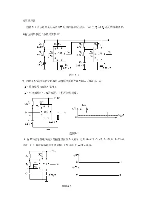
第五章习题1.题图5-1所示电路是用两片555组成的脉冲发生器,试画出Y 1和Y 2两处的输出波形,并标注要紧参数(参数只需估算)。
R 1C 133kR 233k 10题图5-12.题图5-2所示的555按时器组成的单稳态触发器及输入v I 的波形,求: (1)输出信号v O 的脉冲宽度T W ;(2)对应v I 画出v C 、v O 的波形,并标明波形幅度。
v I /V CC /3v Iv O题图5-23.由555按时器组成的多谐振荡器如图5-3所示,已知V DD =12V 、C =μF、R 1=15k Ω、R 2=22k Ω。
试求:(1)多谐振荡器的振荡周期;(2)画出的v C 和v O 波形。
v O /Vv C /V00tR Cv v OR题图5-34.由555按时器、3位二进制加计数器、理想运算放大器A 组成如题图5-4所示电路。
设计数器初始状态为000,且输出低电平V OL =0 V ,输出高电平V OH = V ,R d 为异步清零端,高电平有效。
(1)说明虚框(1)、(2)部份各组成什么功能电路?(2)虚框(3)组成几进制计器? (3)对应CP 画出v O 波形,并标出电压值。
题图5-45.用集成芯片555组成的施密特触发器电路及输入波形i v 如题图5-5所示,要求: (1)求出该施密特触发器的阈值电压V T +、V T -;(2)画出输出v o 的波形。
v I /V tv O /Vv v O题图5-56.用集成按时器555组成的电路及可产生的波形如题图5-6(a )、(b )所示,试回答: (1)该电路的名称;(2)指出(b )图中v C 波形是1~8引脚中,哪个引脚上的电压波形; (3)求出矩形波的宽度t W 。
v Iv O 0.3v v(a ) (b )题图5-67.题图5-7为简易门铃电路,设电路中元器件参数适合,R >>R 1,S 为门铃按钮,当按钮按一下放开后,门铃可响一段时刻。
第5章习题参考答案Problem 5.1library ieee;use ieee.std_logic_1164.all;package my_data_type isconstant m: integer :=8;type vector_array is array (natural range<>) ofstd_logic_vector(m-1 downto 0);end my_data_type;library ieee;use ieee.std_logic_1164.all;use work.my_data_type.all;entity n_mux isgeneric (n: integer :=8);port( datain: in vector_array(0 to n-1) ;sel: in integer range 0 to n-1;dataout: out std_logic_vector( m-1 downto 0)); end;architecture bhv of n_mux isbegindataout<=datain(sel);end;Problem 5.2方法一:利用简单赋值语句设计library ieee;use ieee.std_logic_1164.all;entity priority_encoder isport(x:in std_logic_vector(7 downto 1);y:out std_logic_vector(2 downto 0));end;architecture bhv of priority_encoder isbeginy(2)<=x(7) or x(6) or x(5) or x(4);y(1)<=x(7) or x(6) or (( not x(5) and not x(4)) and (x(3) or x(2)));y(0)<=x(7) or (not x(6) and (x(5) or (not x(4) and (x(3) or (not x(2) and x(1))))));end;方法二:利用WHEN语句设计library ieee;use ieee.std_logic_1164.all;entity priority_encoder isport(x:in std_logic_vector(7 downto 1);y:out std_logic_vector(2 downto 0));end;architecture bhv of priority_encoder isbeginy<="111" when x(7)='1' else"110" when x(6)='1' else"101" when x(5)='1' else"100" when x(4)='1' else"011" when x(3)='1' else"010" when x(2)='1' else"001" when x(1)='1' else"000";end;Problem 5.4library ieee;use ieee.std_logic_1164.all;use ieee.std_logic_unsigned.all;entity adder8 isport(a,b:in std_logic_vector(7 downto 0);cin:in std_logic;sum:out std_logic_vector(7 downto 0);cout:out std_logic);end;architecture bhv of adder8 issignal a0,b0,cin0, s:std_logic_vector(8 downto 0); begina0<='0'&a; b0<='0'&b; cin0<="00000000"&cin; s<=a0+b0+cin0;sum<=s(7 downto 0);cout<=s(8);end;Problem5.5library ieee;use ieee.std_logic_1164.all;use ieee.std_logic_arith.all;use ieee.std_logic_unsigned.all;use ieee.std_logic_signed.all;entity add_sub isport(a,b:in unsigned(7 downto 0);sel:in bit_vector(1 downto 0);sum:out std_logic_vector(8 downto 0)); end;architecture bhv of add_sub issignal temp1,temp2:unsigned (8 downto 0); signal temp3,temp4:signed(8 downto 0);--signal an,as,sn,ss:std_logic_vector(8 downto 0);signal a0,b0:signed (7 downto 0);signal cin0:std_logic_vector(7 downto 0);begina0<=conv_signed(a,8);b0<=conv_signed(b,8);temp1<=conv_unsigned((a+b),9);temp2<=conv_unsigned((a-b),9);temp3<=conv_signed((a0+b0),9);temp4<=conv_signed((a0-b0),9);sum<=conv_std_logic_vector(temp1,9)when sel="00" else conv_std_logic_vector(temp3,9)when sel="01" elseconv_std_logic_vector(temp2,9)when sel="10" elseconv_std_logic_vector(temp4,9);end;Problem 5.6library ieee;use ieee.std_logic_1164.all;entity gray_encoder isgeneric(n: integer:=4) ;port(input:in std_logic_vector(n-1 downto 0);output:out std_logic_vector(n-1 downto 0));end;architecture bhv of gray_encoder isbeginoutput(n-1)<=input(n-1);output(n-2 downto 0)<=input(n-2 downto 0) xor input(n-1 downto 1); end;Problem 5.7(将原题修改后的作业题,要求能够实现连续移位,当shift 信号为0时,保持不变,否则每次左移移位,最低位补0,直到全0为止。
第五章 数字电路基础一、填空题:1.(7-4易)______AB AB +=。
2.(7-4易)_____A AB +=。
3.(7-4中)______A AB +=。
4.(7-4难)___________AB AC BC ++=。
5.(7-2易)逻辑代数有 、 和逻辑非三种基本运算。
6.(7-4易)1____A ⊕=。
7.(7-4易)A ⊙1=__________。
8.(7-2易)如果输入与输出的关系是"有0出1,全1出0",这是 逻辑运算。
"全0出0,有1出1",这是 逻辑运算。
9.(7-2中)异或门的逻辑功能是 、 。
10.(7-1易) 晶体二极管具有____________特性,利用这一特性可作开关电路。
11.(7-1易)晶体二极管从导通到截止需要一段时间,称之为_______________。
12.(7-1易) 晶体三极管通过对其基极电位控制,可使其处于________状态或_______状态。
13.(7-1易) 晶体三极管的U BE _____ U th (填>,<,或=)时,其处于截止状态。
(U th 为三极管发射结导通电压)。
14.(7-1中) 在实验和实际中,可在三极管的基极电阻上并联一个______________来加速管子开启和关闭速度。
15.(7-3易) n 个变量有________个最小项。
16.(7-2易) 三态输出与非门的输出端有三种状态:______,______,______。
17.(7-3中) (127)10=( )2=( )8=( )1618.(7-3中) (254.25)10=( )2=( )8= ( )1619.(7-3难)(2.718)10=( )2(小数点后保留4位)= ( )8=( )1620.(7-4难)AB A C BC ++=_______________。
21.(7-1易)逻辑变量的取值有种,即。
5.11画出图P5.11电路Q端的波形。
设初态为“0”。
图P5.14 图P5.15 5.15 画出图P5.15电路中Q端的波形。
解:Q 端波形如图P5.15所示。
5.16 试作出图P5.16电路中Q A 、Q B 的波形。
解:Q 端波形如图P5.16所示。
R D CP CP ⊕Q 2
Q 1Q 2
A R D
B Q A
Q B
图P5.16 图P5.17
5.17 试作出图P5.17电路中Q 1、Q 2 的波形。
解:Q 端波形如图P5.17所示。
5.18 试作出图P5.18电路中Q 1和Q 2的波形(设Q 1和Q 2的初态均为“0”),并说明Q 1和
Q 2对于CP 2各为多少分频。
解:Q 端波形如图P5.18所示。
Q 1和Q 2对于CP 2都是4分频,即
图P5.18 图P5.19
5.19 已知电路如图P5.19,试作出Q 端的波形。
设Q 的初态为“0”。
解:Q 端波形如图P5.19所示。
5.20 已知输入u I 、输出u O 波形分别如图P5.20所示,试用两个D 触发器将该输入波形u I
转换成输出波形u O 。
解:实现电路如图P5.20所示。
图P5.20
?)
?,(2
22
1==CP Q CP Q f f f f CP 2CP 1Q 1Q 2
CP A Q
u I
u O。
习题参考答案注:参考答案,并不是唯一答案或不一定是最好答案。
仅供大家参考。
第一章习题2. C B A D B A C B A F ⋅⋅+⋅⋅+⋅⋅=3. 设:逻辑变量A 、B 、C 、D 分别表示占有40%、30%、20%、10%股份的四个股东,各变量取值为1表示该股东投赞成票;F 表示表决结果,F =1表示表决通过。
F =AB +AC +BCD4. 设:A 、B 开关接至上方为1,接至下方为0;F 灯亮为1,灯灭为0。
F =A ⊙B5. 设:10kW 、15kW 、25kW 三台用电设备分别为A 、B 、C ,设15kW 和25kW 两台发电机组分别为Y 和Z ,且均用“0”表示不工作,用“1”表示工作。
C AB Z BA B A Y ⋅=⋅=6.输入为余3码,用A 、B 、C 、D 表示,输出为8421BCD 码,用Y 0、Y 1、Y 2、Y 3表示。
D C A B A Y CB DC BD B Y DC Y DY ⋅⋅+⋅=⋅+⋅⋅+⋅=⊕==32107. 设:红、绿、黄灯分别用A 、B 、C 表示,灯亮时为1,灯灭时为0;输出用F 表示,灯正常工作时为0,灯出现故障时为1。
C A B A C B A F ⋅+⋅+⋅⋅=8. D C B D A H DC B AD C B A D C B A D C B A G DC B AD C A B A F DC B A E ⋅⋅+⋅=⋅⋅⋅+⋅⋅⋅+⋅⋅⋅+⋅⋅⋅=⋅⋅⋅+⋅⋅+⋅=⋅⋅⋅=第二章习题1. 设:红、绿、黄灯分别用A 、B 、C 表示,灯亮时其值为1,灯灭时其值为0;输出报警信号用Y 表示,灯正常工作时其值为0,灯出现故障时其值为1。
AC AB C B A Y ⋅⋅=2. 设:烟、温度和有害气体三种不同类型的探测器的输出信号用A 、B 、C 表示,作为报警信号电路的输入,有火灾探测信号时用1表示,没有时用0表示。
报警信号电路的书躇用Y 表示,有报警信号时用1表示,没有时用0表示。
第五章答案5.5ZQ Q XQ Q X Q Q X Q Q X QQ X K Q X J Q Q Q X Q X Q XQ Q Q X Q XQ K Q X J n n =∙++∙=∙+∙=∴∙==∙++∙=+∙∙=∴==++2121212112121221121221112121,,下降沿触发CP X Q1Q25.632113321321121223111131,1,,,1,Q Q Q Q K Q Q J Q Q Q Q K J Q Q Q K Q J n n n ∙=∴==⊕=∴==∙=∴==+++000,100,010,011,111,000 5进制计数器 5.83321132212113111231CP Q Q Q Q CP Q Q CP Q Q Q Q CP CP CP n n n ∙=∙=∙∙===+++000,100,010,011,111,000 5进制 5.92212111100211012100211CP Q Q CP Q Q CP Q Q Q Q Q CP Q Q Q Q CP n n n n ∙=∙=∙==→+=++++能自启动的7进制计数器5.101221120Q CP Q A D Q D AQ D =+===A=0时Q2翻转,Q0不变,Q1不变 A=1时Q2=Q0=1,Q1不变 A 发生变化才会引起变化 5.1174163是同步清零同步置数的思维二进制计数器 只有S0时Z 为0,所以012Q Q Q Z ++=11210121010012X Q Q X Q Q Q X Q Q X Q Q Q LD +++= 0112122X Q X Q Q Q D ++= 11010121X Q X Q Q Q Q D ++= 00100120X Q X Q Q Q Q D ++= 03=D按照表达式就可以画出电路图(略) 5.12两个74161都连成0000,0001,0010,0011,0100,1000,1001,1010,1011,1100循环的10进制计数器,右边只有在左边为1100时才计一个数 100进制计数器 5.137490是异步清0,先连成10进制,当输出为0111清0。
第五章锁存器和触发器1、Q n 1二S RQ n, SR = O2、Q n, 03、324、TCP J I I I I I I I7、4-13题解图8、D= A 二BCP_ I~I I~I I~I I~I I~LI Iz卄I TH 1D i - I i i1 . I | , __ L,I ■ I ______第六章时序逻辑电路1、 输入信号,原来的状态2、 异3、 n 5、反馈清零、反馈置数扌-6、N乂—LJ UU 仑厂 II ~ 7、状态方程和输出方程:㈣ =A®Q'tZ^AQ&激励方程A =Kq = A &/. =e 0=i 状态方程0:戚;忧"无©土死输出方程Z=AQ1Q0根据状态方程组和输出方程可列出状态表,如表题解6 . 2 . 4所示,状态图如图题解2. 4 所示。
Q - M?; + M V ;* Q ; = + “:14、图题解6.2.4Q;・枫"烟00保持,01右移10左移11并行输入当启动信号端输人一低电平时,使S仁1 ,这时有So= Sl= 1 ,移位寄存器74HC194执行并行输人功能,Q3Q2Q1Q0 = D3D2D1D0 = 1110。
启动信号撤消后,由于Q°= 0,经两级与非门后,使S仁0 ,这时有S1S0= 01 ,寄存器开始执行右移操作。
在移位过程中,因为Q3Q2、Q1、Q0中总有一个为0,因而能够维持S1S0=01状态,使右移操作持续进行下去°其移位情况如图题解6, 5, 1所示。
该电路能按固定的时序输出低电平脉冲,是一个四相时序脉冲产生电路。
-JT AAA TL幺I15、状态方程为儿⑷儿個)X(O24、解:74HC194功能由S1S0控制。
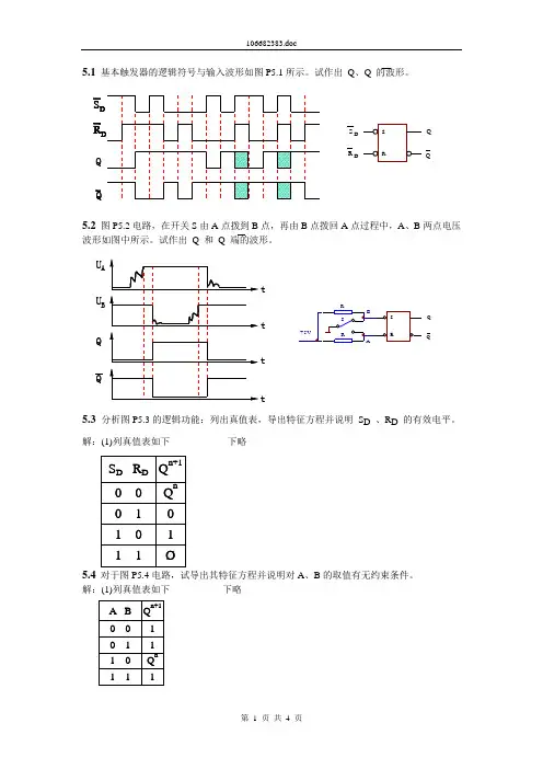
本章习题5.1分析图题4.1a 电路的逻辑功能,列出逻辑功能表,画出R、S 输入图b 信号时的输出波形。
题5.1 逻辑功能表解: 见题5.1 逻辑功能表和波形图。
5.2画出图题5.2各触发器在时钟脉冲作用下的输出波形。
(初态为“0”) 解:波形见题5.2图。
5.3 画出图题4.3中各不同触发方式的D 触发器在输入信号作用下的输出波形 (初态为0)。
Q n S R Q n+1 Q —n+1 功能0 1 0 1 0 置位1 1 0 1 0 置位00 1 0 1 复位10 1 0 1 复位00 0 0 1 保持10 0 1 0 保持0 1 1 1 1 非法11111非法解:波形见题5.3图。
5.4 图题5.4a由CMOS或非门和传输门组成的触发器,分析电路工作原理,说明触发器类型。
如果用两个图a的电路构成图b电路,说明图b电路是什么性质的触发器。
解:图a为同步D触发器,CP为使能控制,低电平有效。
当CP=“0”时,TG1通、TG2断,触发器根据D信号改变状态;当CP=“1”时,TG1断、TG2通,触发器状态保持。
逻辑符号如图5.2a。
图b为主从D触发器,时钟CP的上升沿有效,逻辑符号如图5.2b。
5.5 画出图题5.5(a)所示电路在输入图(b)信号时的输出波形。
解:当A=“1”时,CP的下降沿使Q=“1”。
当Q=“1”且 CP =“1”时,Q复位。
波形见题5.5图。
5.6画出图题5.6(a)电路的三个输出Q2、Q1、Q0在图(b)信号输入时的波形变化图(初始状态均为“0”)。
分析三个输出信号和输入信号的关系有何特点。
解:波形见题5.6图。
输出信号按位序递增顺序比输入滞后一个CP周期。
5.7 画出图题5.7所示电路的三个输出Q2、Q1、Q0在时钟脉冲作用下波形变化图(初始状态均为“0”)。
若三个输出组成三位二进制码,Q2为最高位,分析输出码和时钟脉冲输入个数之间的关系。
解:波形见题5.7图,输出码随时钟输入递减:“000”→“111”→“110” →“101” →“100” →“011” →“010” →“011” →“001” →“000”,每8个时钟周期循环一次。
第五章同步时序电路习题答案: 5.1 解:n n Q X D Q ⊕==+1 n XQ Z =5.2 解:n XQ J 01= X K =1 X J =0 n XQK 10=n n n n n n XQ XQ XQ Q XQ Q 1011011+=+=+ n n n n n n XQ Q X Q XQ Q X Q 1001010+=+=+ n n Q XQ Z 10=Q 1n Q 0n X Q 1n+1Q 0n+1 Z 0 0 0 0 0 1 0 0 10 1 1 0 1 0 0 0 1 0 1 1 1 0 1 1 0 0 0 0 1 1 0 1 1 1 1 1 1 0 0 0 1 1 1 1 1 1 05.3 解:n n n Q Q D Q 02010==+n n n n n n n Q Q Q Q Q Q D Q 010101111⊕=+==+ n n n n Q Q Q D Q 012212==+1/10/1 X 010 1 0/1 1/1 1/1 0/0n Q+n n Q Z初态为“1”nn Q Q 01X/ZX1+n Q 0+n Q ZX1+n Q 0+n Q Z Q 2n Q 1n Q 0n Q 2n+1Q 1n+1Q 0n+1 0 0 0 0 0 10 0 1 0 1 0 0 1 0 0 1 1 0 1 1 1 0 0 1 0 0 0 0 0 1 0 1 0 1 0 1 1 00 1 0 Q 212+n Q 逻辑功能:可自启动的同步五进制加法计数器。
5.45.55.6 解:(1)当X 1X 2=“00”;初始状态为“00”时:112=+n Q 121==n Q J 1111==X J Kn n Q Q 111=+逻辑功能:电路实现2分频。
(2)当X 1X 2=“01”;初始状态为“00”时:n Q J 21= 1111==X J K n n n Q Q Q 1211=+n Q J 12= 1112==X Q K n n n n Q Q Q 1212=+逻辑功能: 电路实现3分频。
(3)当X 1X 2=“11”;初始状态为“00”时: n Q J 21= n Q X J K 2111==n n n n n n Q Q Q Q Q Q 2121211=+=+ n Q J 12= n n Q X Q K 1112== n n n n n n Q Q Q Q Q Q 1212112=+=+ 逻辑功能: 电路实现4分频。
Y 3 Y 2 Y 1 Y 0n n n Q Q Q J 1234= nQ K 14=n n Q Q J 143= nn Q Q K 123=n n n Q Q Q J 1342= n Q K 12=111==K J n n n n n n n Q Q Q Q Q Q Q 14123414+=+n n n n n n n Q Q Q Q Q Q Q 31213413)(++=+nn n n n n n Q Q Q Q Q Q Q 12123412)(++=+14+n Q CP13+n Q 12+n Q 11+n Q Zn n Q Q 111=+nn n n Q Q Q Q Z 1234=时序图:11+n Q 12+n Q 11+n Q 12+n Q “1”5.7 (1)(2)Q D 端输出是12分频,占空比是50%。
D C B Q Q Q K ⊕=)(5.8 (1) 基本R-S 触发器 ( × ); (2) 同步R-S 触发器( × ); (3) 主从J-K 触发器 ( 能 ); (4) 维持阻塞D 触发器(能 ); (5) 边沿J-K 触发器 ( 能 ); (6) CMOS 主从D 触发器(能 )。
5.9 根据题意D 2=XQ XD 0nI ⋅,很容易画出下面的逻辑图:5.10 解:四种状态应使用2个触发器。
设:Q 1=Y 1,Q 0=Y 01) 用D 触发器设计;XQ Q X Q Q X Q Q X Q Q X Q Q Q D n ⊕⊕=+++==+010*******11 0100Q Q D n ==+01Q Q Z = 2)用J —K 触发器设计;XQ Q X Q Q X Q Q X Q Q Q n 010*******+++=+=1010)(Q X Q Q X Q ⊕+⊕X Q K J ⊕==011010Q Q n =+ 122==K J 01Q Q Z =5.11 解:用J —K 触发器设计一个4进制计数器,Q 1Q 0为变量译码器的输入。
n n n n n Q Q Q Q Q 101011+=+ n Q K J 011== n n Q Q 010=+ 100==K JDnCn Bn An Q Q Q Q n Q 1n Q 011+n Q10+n Q 0 0 0 1 0 1 1 0 1 11 0 1 1 0 0DQ QQ Q QQCPFF0FF1FF2DD XD I5.12RCP1+nQ0+nQY0Y1Y2Y3nQJ12=n21XQQKnn12+=nnn112nn021n25.13 解:设S 0:初始及检测成功状态;S 1:输入一个“1”状态;S 2:输入“10”状态;S 3:输入“101”状态;X :输入;Z :输出。
(1)状态图 (2)状态表 (3)状态分配方案(4)状态方程 方案一:方案二:方案三、状态X 0 1 S 1 S 0 S 2 S 3S 0/0 S 2/0 S 0/0 S 2/0S 1/0 S 1/0 S 3/0 S 0/11 2 3 S 0 00 00 01S 1 01 01 00S 2 11 10 10S 3 10 11 11X Z 0 0 0 0 0 0 0 × 0 ×0 0 1 0 10 0 × 1 ×0 1 0 1 1 0 1 × ×00 1 1 0 1 0 0 × ×01 1 0 0 0 0 × 1 ×11 1 1 1 0 0 × 0 ×1 1 0 0 1 1 0 × 0 1 ×1 0 1 0 0 1 × 1 0 ×n Q 1 n Q 0 11+n Q 10+n Q 0011K J K J X/Z X Q Q X Q K J n n n 01011+==XQ Q Q Q X Q K J n n n n n 0101100++== X Z 0 0 0 0 0 0 0 × 0 ×0 0 1 0 1 0 0 × 1 ×0 1 0 1 0 0 1 × ×10 1 1 0 1 0 0 × ×01 0 0 0 0 0 × 1 ×01 0 1 1 1 0 × 0 1×1 1 0 1 0 0 × 0 ×11 1 1 0 0 1 × 1 ×1n Q 1 n Q 0 11+n Q 10+n Q 0011K J K J X Q X Q X Q K J n n n 01000++==XQ Q X Q Q X Q Q K J n n n n n n 01010111++== X Z 0 1 0 0 1 0 0 × ×00 1 1 0 00 0 × ×10 0 0 1 00 1 × 0×0 0 1 0 0 0 0 × 0×1 0 0 0 1 0 × 1 1×1 0 1 1 1 0 × 0 1×1 1 0 1 00 × 0 ×11 1 1 0 1 1 × 1 ×0n Q 1 n Q 0 11+n Q10+n Q 0011K J K J X Q Q X Q K J n n n 01011+==从JK 的卡诺图可以看出电路的 简化结果相似,以方案三画逻辑电路5.14 解:从时序图可得出状态图为:方法一:若将i φ看作触发器的输出,三个触发器不可能有这样的状态,因此应有6个状态,并且在传输“1”,可用6个触发器构成移位寄存器型计数器。
其中533211,,Q Q Q ===φφφ。
此时,状态图为: 逻辑图:方法二:用3个触发器构成6进制计数器,123φφφ为输出。
同理:n n Q Q 123=φ n n n Q Q Q 0122=φ n n Q Q 011=φn n n n n n Q Q Q Q Q Q 543210123/φφφ5 n n n Q Q Q 012 123/φφφ 0 0 00 0 1 0 0 00 0 1 0 1 1 0 0 10 1 10 1 0 0 0 00 1 0 1 1 0 0 1 01 1 0 1 0 0 0 0 01 0 00 0 0 1 0 0n n n Q Q Q 012101112+++n n n Q Q Q 123φφφnn n Q Q Q D 12100==+n n n n Q Q Q Q D 120111+==+nn n Q Q Q D 01122==+X/Y 1Y 2Z5.15 解:方法一:从时序图中可以看出将Y 1、Y 2、Z 为输出时,每经过8个时钟为一个循环。
其状态图为: 若以自然态序状态分配,状态表为:X Q Q X Q X Q Q D n n n n n 0110122++==+ 或 n n n n n n n n Q Q Q Q Q Q Q Q D 0121202122++==+同理,从卡诺图可以求出: 01111Q Q Q D n ⊕==+ n n Q Q D 0100==+n Q Y 01= X Q Q Q Q Q Q Y n n n n n 101122++= X Q Q X Q Q Z n n n n 0101+=方法二:从时序图中可以看出Y 1Y 2的状态为00→11→01→10→00。
设:n n Q Y Q Y 0211==;则状态图、状态表为: n n Q Q D 1111==+ 同理: X Q Q Q D n n n ⊕⊕==+01100X Q Q X Q Q Z n n n n 0101+=显然,方法二的结果比方法一的结果要简单得多。
其逻辑图为:5.16 解:ZW 的状态为00、01、10、11,所以设:输出Z=Q 1;W=Q 0;输入:Xn n Q Q 01 X/Z状态图 状态表X Q X Q Q D n n n 10111+==+5.17解: 1、状态转换图2.1253640713128151491011Qd 对CP 十分频,Qd 的占空比是50%。