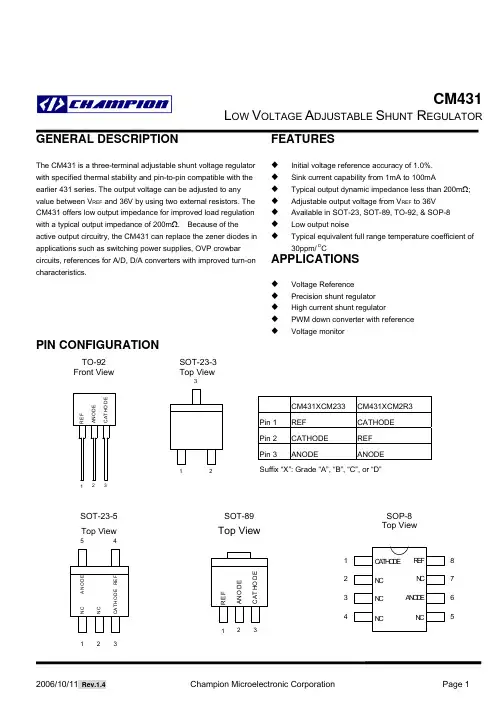
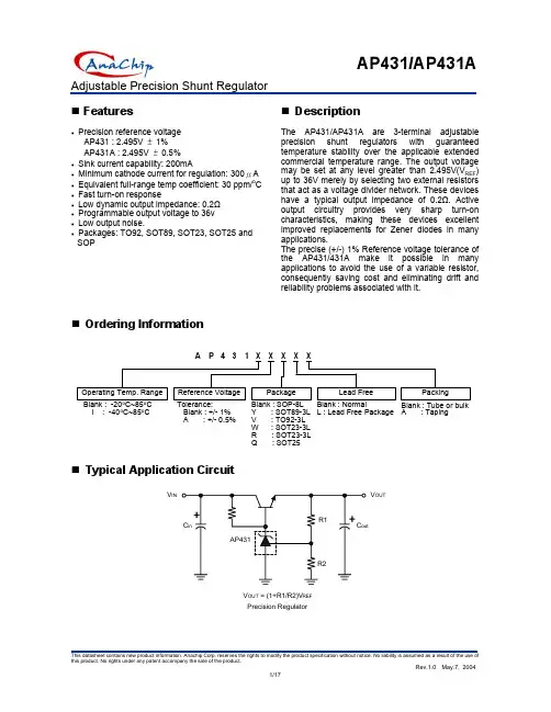
APL431LAYC-TBL中文资料
- 格式:pdf
- 大小:222.52 KB
- 文档页数:15
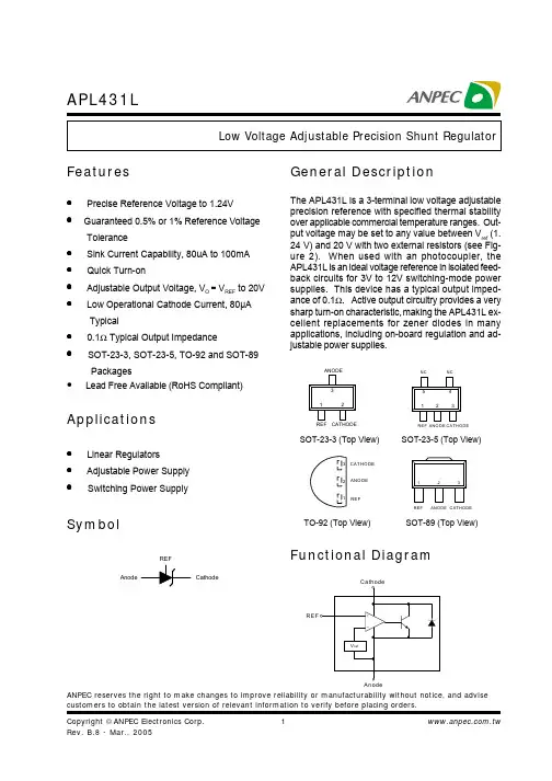
APL431LANPEC reserves the right to make changes to improve reliability or manufacturability without notice, and advise customers to obtain the latest version of relevant information to verify before placing orders.FeaturesGeneral DescriptionApplicationsThe APL431L is a 3-terminal low voltage adjustable precision reference with specified thermal stability over applicable commercial temperature ranges. Out-put voltage may be set to any value between V ref (1.24 V) and 20 V with two external resistors (see Fig-ure 2). When used with an photocoupler, the APL431L is an ideal voltage reference in isolated feed-back circuits for 3V to 12V switching-mode power supplies. This device has a typical output imped-ance of 0.1Ω. Active output circuitry provides a very sharp turn-on characteristic, making the APL431L ex-cellent replacements for zener diodes in many applications, including on-board regulation and ad-justable power supplies.• Precise Reference Voltage to 1.24V• Guaranteed 0.5% or 1% Reference VoltageTolerance• Sink Current Capability, 80uA to 100mA • Quick Turn-on• Adjustable Output Voltage, V O = V REF to 20V • Low Operational Cathode Current, 80µATypical• 0.1Ω Typical Output Impedance• SOT-23-3, SOT-23-5, TO-92 and SOT-89Packages• Lead Free Available (RoHS Compliant)• Linear Regulators• Adjustable Power Supply • Switching Power SupplySymbolFunctional DiagramSOT-23-3 (Top View)REF ANODECATHODE123SOT-89 (Top View)REFANODE CATHODE123REFANODECATHO DE321TO-92 (Top View)CathodeAnodeREFREF NCCATHODENCANODE 12345SOT-23-5 (Top View)APL431LOrdering and Marking InformationNotes: ANPEC lead-free products contain molding compounds/die attach materials and 100% matte in plate termination finish; which are fully compliant with RoHS and compatible with both SnPb and lead-free soldiering operations. ANPEC lead-free products meet or exceed the lead-free requirements of IPC/JEDEC J STD-020C for MSL classification at lead-free peak reflow temperature.Absolute Maximum RatingsAPL431LElectrical Characteristics T A = 25°C ( unless otherwise noted)Notes : 1.Full temperature range is 0°C to 70°C for APL431LXXC,and -40°C to 85°C for APL431LXXl.Test FiguresFigure 1. Test Circuit for V KA =V REF , V O =V KA =V REF Figure 3. Test Circuit for I K(off)V INV oAPL431LTest Figures (Cont.)Figure 2. Test Circuit for V KA >V REF ,V O = V KA = V REF × (1+R 1/R 2) + I REF × R 1V INV oApplication SchematicV oVPrecision Voltage ReferenceV oV INPrecision High-Current Series RegulatorNotes for Application Circuits:1) T o improve the stability of output voltage, a 0.1µF capacitor between cathode and anode of APL431L is strongly recommended.2)Set V OUT according to the following equation: V OUT = V REF (1+R1/R2)+l REF R13)Choose the value for R B as follows:A)The maximum limit for R B should be such that the cathode current(l K ) is greater than the mini mum operating current (80µA) at V IN(MIN). B)The minimum limit for RB should be such that the cathode current (l K ) does not exceed 100mA under all load conditions, and the instantaneous turnon value for lk does not exceed 150mA. Both of the following conditions must. be met: V IN(MAX)150mA V IN(MAX)-V OUTl OUT(MIN)+100mA(to limit instantaneous turn-on l K ) R B,Min ≥(to limit l K under normal operating conditions)R B,Min ≥0.080.100.120.140.160.18-50-252550751001251501.221.231.241.251.26-50-25255075100125150Junction Temperature (°C)R e f e r e n c e V o l t a g e (V )R e f e r e n c e I n p u t C u r r e n t (µA )Junction Temperature (°C)Referemce Voltage vs.Junction TemperatureReference Input Current vs.Junction TemperatureAPL431L0.10.20.30.40.5-50-252550751001251500Sµ01V5Sµ3V0Sµ5Sµ01V03VTypical CharacteristicsInputR a t i o o f D e l t a R e f e r e n c e V o l t a g e t oJunction Temperature (°C)O f f S t a t e C a t h o d e C u r r e n t (µA )Off State Cathode Current vs.Junction Temperature/∆V vs. Junction TemperatureI KA =1mAOutputInputOutputT A =25°CI KA =0.1mAT A =25°CAPL431L1020304050607080901000.00010.0010.010.11-100102030405060501001502002503003500.010.1110100101001000100001000001000000Typical CharacteristicsFrequency (Hz)Z k a (Ω)Frequency (Hz)G a i n (d B )P h a s e S h i f t (d e g r e e )Gain vs. Phase Shift vs. FrequencyZka vs. FrequencyLoad Capacitance (µF)I k (m A )Stability Boundary ConditionsAPL431LPackage Information SOT-23APL431LPackage Information SOT-23-5APL431LPackage Information TO-92APL431LPackage InformationSOT-89 (Reference EIAJ ED-7500A Reg stration SC-62)APL431LPhysical SpecificationsT LT P25T e m p e r a t u r eTim eReflow Condition (IR/Convection or VPR Reflow)Classificatin Reflow ProfilesAPL431LReliability Test ProgramCarrier Tape & Reel DimensionsAPL431LCarrier Tape & Reel DimensionsCarrier Tape & Reel Dimensions(mm)APL431LCover Tape DimensionsCustomer ServiceAnpec Electronics Corp.Head Office :5F, No. 2 Li-Hsin Road, SBIP,Hsin-Chu, T aiwan, R.O.C.T el : 886-3-5642000Fax : 886-3-5642050Taipei Branch :7F, No. 137, Lane 235, Pac Chiao Rd.,Hsin Tien City, Taipei Hsien, Taiwan, R. O. C.T el : 886-2-89191368Fax : 886-2-89191369。