数字逻辑_chapter3_答案
- 格式:pdf
- 大小:114.78 KB
- 文档页数:22
第一章开关理论基础1.将下列十进制数化为二进制数和八进制数十进制二进制八进制49 110001 6153 110101 65127 1111111 177635 1001111011 11737.493 111.1111 7.7479.43 10011001.0110111 231.3342.将下列二进制数转换成十进制数和八进制数二进制十进制八进制1010 10 12111101 61 751011100 92 1340.10011 0.59375 0.46101111 47 5701101 13 153.将下列十进制数转换成8421BCD码1997=0001 1001 1001 011165.312=0110 0101.0011 0001 00103.1416=0011.0001 0100 0001 01100.9475=0.1001 0100 0111 01014.列出真值表,写出X的真值表达式A B C X0 0 0 00 0 1 00 1 0 00 1 1 11 0 0 01 0 1 11 1 0 11 1 1 1 X=A BC+A B C+AB C+ABC5.求下列函数的值当A,B,C为0,1,0时:A B+BC=1(A+B+C)(A+B+C)=1(A B+A C)B=1当A,B,C为1,1,0时:A B+BC=0(A+B+C)(A+B+C)=1(A B+A C)B=1当A,B,C为1,0,1时:A B+BC=0(A+B+C)(A+B+C)=1(A B+A C)B=06.用真值表证明下列恒等式(1) (A⊕B)⊕C=A⊕(B⊕C)A B C (A⊕B)⊕C A⊕(B⊕C)0 0 0 0 00 0 1 1 10 1 0 1 10 1 1 0 01 0 0 1 11 0 1 0 01 1 0 0 01 1 1 1 1所以由真值表得证。
(2)A⊕B⊕C=A⊕B⊕CA B C A⊕B⊕C A⊕B⊕C0 0 0 1 10 0 1 0 00 1 0 0 00 1 1 1 11 0 0 0 01 0 1 1 11 1 0 1 11 1 1 0 07.证明下列等式(1)A+A B=A+B证明:左边= A+A B=A(B+B)+A B=AB+A B+A B=AB+A B+AB+A B=A+B=右边(2)ABC+A B C+AB C=AB+AC证明:左边= ABC+A B C+AB C= ABC+A B C+AB C+ABC=AC(B+B)+AB(C+C)=AB+AC=右边(3)EDCCDACBAA)(++++=A+CD+E 证明:左边=EDCCDACBAA)(++++=A+CD+A B C+CD E=A+CD+CD E=A+CD+E=右边(4) C B A C B A B A ++=C B C A B A ++ 证明:左边=C B A C B A B A ++=C B A C AB C B A B A +++)( =C B C A B A ++=右边8.用布尔代数化简下列各逻辑函数表达式9.将下列函数展开为最小项表达式 (1) F(A,B,C) = Σ(1,4,5,6,7)(2) F(A,B,C,D) = Σ(4,5,6,7,9,12,14) 10.用卡诺图化简下列各式(1)C AB C B BC A AC F +++=化简得F=C(2)C B A D A B A D C AB CD B A F++++=F=D A B A +(3) F(A,B,C,D)=∑m (0,1,2,5,6,7,8,9,13,14)化简得F=D BC D C A BC A C B D C ++++(4) F(A,B,C,D)=∑m (0,13,14,15)+∑ϕ(1,2,3,9,10,11)化简得F=AC AD B A ++11.利用与非门实现下列函数,并画出逻辑图。
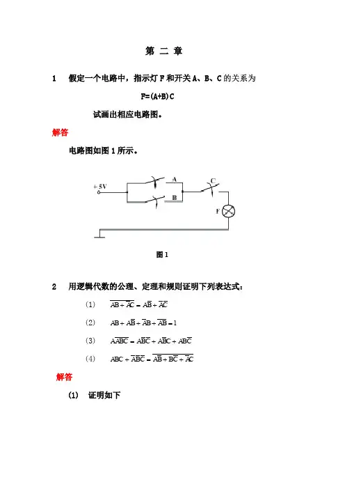
第三章(组合逻辑电路)作业及答案1、写出图3-1所示组合逻辑电路中输入输出的逻辑关系式和真值表。
图3-1:组合逻辑电路逻辑图解:(1)C A A AC B AY +=++=1(2)D B C B A CD B A CD B A D BD CD A B A Y ++=++=+=++=)(2 2、试分析图3-2所示组合逻辑电路,写出其逻辑函数表达式。
若设S 1﹑S 0为功能控制信号,A ﹑B 为输入信号,L 为输出,说明当S 1﹑S 0取不同信号值时,电路所实现的逻辑功能。
图3-2:组合逻辑电路逻辑图3、试用与门、或门和非门,或者与门、或门和非门的组合来实现如下各逻辑函数关ABS 1S=1=1&=1系,画出相应的逻辑电路图。
(1)1Y AB BC=+(2)2Y A C B=+()(3)3Y ABC B EF G=++()&&1≥Y1.1ABC.&1≥Y2.1ABC&1≥1≥&&1ABC.EFG.Y3...4、试用门电路设计4线-2线优先编码器,输入、输出信号都是高电平有效,要求任一按键按下时,G S为1,否则G S=0;还要求没有按键按下时,E O信号为1,否则为0。
5、试用逻辑门电路设计一个2选1数据选择器,输入信号为A、B,选择信号为S,输出信号为Y,要求写出真值表、逻辑函数表达式和画出逻辑电路图。
6、某公司3条装配线各需要100kW电力,采用两台发电动机供电,一台100kW,另外一台是200kW,3条装配线不同时开工,试设计一个发电动机控制电路,可以按照需求启动发电动机以达到节电的目的。
7、图3-3是由3线/8线译码器74LS138和与非门构成的组合逻辑电路,试写出P和P2的逻辑表达式,并列出真值表,说明其逻辑功能。
1BIN/OCT01201234567B AC 10074LS138P 1P 2图3-3 组合逻辑电路图8、试用3线-8线译码器74LS138和与非门实现以下多输出函数:1F AB C AB BC AC =++(,,) ∑=),,,(),,(75422m C B A F9、图3-4是由八选一数据选择器74LS151构成的组合逻辑电路,试写出当G 1G 0为各种不同取值时输出Y 与输入A 、B 的逻辑函数表达式。
第三章 时序逻辑1.写出触发器的次态方程,并根据已给波形画出输出 Q 的波形。
解:2. 说明由RS 触发器组成的防抖动电路的工作原理,画出对应输入输出波形解:3. 已知JK 信号如图,请画出负边沿JK 触发器的输出波形(设触发器的初态为0)4. 写出下图所示个触发器次态方程,指出CP 脉冲到来时,触发器置“1”的条件。
解:(1),若使触发器置“1”,则A 、B 取值相异。
(2),若使触发器置“1”,则A 、B 、C 、D 取值为奇数个1。
5.写出各触发器的次态方程,并按所给的CP 信号,画出各触发器的输出波形(设初态为0)解:6. 7. 1)(1=+++=+c b a Qa cb Q nn B A B A D +=D C B A K J ⊕⊕⊕==Q AQ B Q D Q C Q E Q F Q G Q H28. 作出状态转移表和状态图,确定其输出序列。
解:求得状态方程如下 故输出序列为:000119. 用D 触发器构成按循环码(000→001→011→111→101→100→000)规律工作的六进制同步计数器解:先列出真值表,然后求得激励方程PS NS 输出N0 0 0 0 0 1 00 0 1 0 1 1 0 0 1 1 1 1 1 0 1 1 1 1 0 1 0 1 0 1 1 0 0 0 1 0 0 0 0 0 1化简得:逻辑电路图如下:10. 用D 触发器设计3位二进制加法计数器,并画出波形图。
n Q 2n Q 1n Q 012+n Q 11+n Q 10+n Q311. 用下图所示的电路结构构成五路脉冲分配器,试分别用简与非门电路及74LS138集成译码器构成这个译码器,并画出连线图。
解:先写出激励方程,然后求得状态方程得真值表得状态图若用与非门实现,译码器输出端的逻辑函数为:若用译码器74LS138实现,译码器输出端的逻辑函数为:12若将下图接成12进制加法器,预置值应为多少?画出状态图及输出波形图。
3 33习 题1.解: CO =AB +BC +ACAC BC AB C B A ABC CO C B A ABC S +++++=+++=)()(AC BC AB C B A ABC )(+++=AC BC AB C AC BC AB B AC BC AB A ABC +++= A B AB C AC C A B C BC B A ABC +++= C B A C B A C B A ABC +++=真值表A B C S CO A B C S CO 0 0 0 0 0 1 0 0 1 0 0 0 1 1 0 1 0 1 0 1 0 1 0 1 0 1 1 0 0 1 011111111电路功能:一位全加器,A 、B 为两个加数,C 为来自低位的进位,S 是相加的和,CO 是进位。
2.解:处于工作状态的译码器C 、D 应输入的状态C D ① 0 0 ② 0 1 ③ 1 0 ④11逻辑功能:由74LS139构成的4线—16线译码器3.解:由图可见,74HC138的功能扩展输入端必须满足E 1=1、032==E E 才能正常译码,因此E 1=A 3=1;542A A E =,即A 4=1,A 5=1; 0763=+=A A E ,即A 6=0,A 7=0。
所以,该地址译码器的译码地址范围为A 7A 6A 5A 4A 3A 2A 1A 0=00111A 2A 1A 0=00111000~3 3400111111,用十六进制表示即为38H ~3FH 。
输入、输出真值表如表P3.3-1所示。
表3.3-1 地址译码器的真值表4.解:由图写出逻辑函数并化简,得02460246L Y Y Y Y Y Y Y Y A BC ABC ABC ABC C ==+++=+++=5. 解:F AB B C A B C AB C ABC ABC =+=+++3 359.解:4选1数据选择器的逻辑表达式为: 301201101001D A A D A A D A A D A A Y +++=将A 1=A ,A 0=B ,D 0=1,D 1=C ,C D =2,D 3=C 代入得 ABC C B A BC A C B A C B A ABC C B A BC A B A Y ++++=+++=根据表达式可画出波形图:C ABL10.解:(1)写出逻辑函数表达式: C AB C B A BC A C B A C B A L ++++=(2)用卡诺图化简3 3611.解:567m m m ABC C B A ABC C AB AC AB L ++=+++=+=13. 解:D C B D C D D C A D C B D C C A F +++=++=)(0⋅+++=+++=CD D C D C A D C AB D C B D C D C A D C A令A 1=C ,A 0=D ,AB D =0,A D =1,D 2=1,D 3=0 连线图:14. 解:3 371。
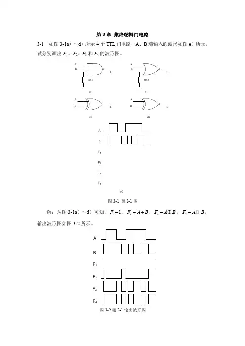
第3章集成逻辑门电路3-1 如图3-1a)~d)所示4个TTL门电路,A、B端输入的波形如图e)所示,试分别画出F1、F2、F3和F4的波形图。
A1A234a)b)c)d)F1F2F3F4BAe)图3-1 题3-1图解:从图3-1a)~d)可知,11F=,2F A B=+,3F A B=⊕,4F A B= ,输出波形图如图3-2所示。
F1F2F3F4AB图3-2题3-1输出波形图3-2 电路如图3-3a )所示,输入A 、B 的电压波形如图3-3b )所示,试画出各个门电路输出端的电压波形。
1A 23b)a)AB图3-3 题3-2图解:从图3-3a )可知,1F AB =,2F A B =+,3F A B =⊕,输出波形如图3-4所示。
F 1F 2F 3AB图3-4 题3-2输出波形3-3在图3-5a )所示的正逻辑与门和图b )所示的正逻辑或门电路中,若改用负逻辑,试列出它们的逻辑真值表,并说明F 和A 、B 之间是什么逻辑关系。
b)a)图3-5 题3-3图解:(1)图3-5a )负逻辑真值表如表3-1所示。
表3-1 与门负逻辑真值表F 与A 、B 之间相当于正逻辑的“或”操作。
(2)图3-5b )负逻辑真值表如表3-2所示。
表3-2 或门负逻辑真值表F 与A 、B 之间相当于正逻辑的“与”操作。
3-4试说明能否将与非门、或非门和异或门当做反相器使用?如果可以,各输入端应如何连接?解:与非门、或非门和异或门经过处理以后均可以实现反相器功能。
1)与非门:将多余输入端接至高电平或与另一端并联; 2)或非门:将多余输入端接至低电平或与另一端并联;3) 异或门:将另一个输入端接高电平。
3-5为了实现图3-6所示的各TTL 门电路输出端所示的逻辑关系,请合理地将多余的输入端进行处理。
b)a)AB=A B=+A BC DABC D图3-6 题3-5图解:a )多余输入端可以悬空,但建议接高电平或与另两个输入端的一端相连;b )多余输入端接低电平或与另两个输入端的一端相连;c) 未用与门的两个输入端至少一端接低电平,另一端可以悬空、接高电平或接低电平;d )未用或门的两个输入端悬空或都接高电平。

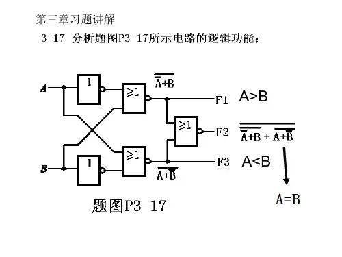
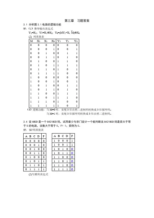
3-1 分析题图3-1所示电路,写出电路输出Y 1和Y 2的逻辑函数表达式,列出真值表,说明它的逻辑功能。
解:由题图3-1从输入信号出发,写出输出Y 1和Y 2的逻辑函数表达式为1Y A B C =⊕⊕ ; 2()()Y A B C AB A B C A =⊕⋅⋅=⊕⋅+B将上式中的A 、 B 、C 取值000~111,分别求出Y 1和Y 2,可得出真值表如题解 表3-1所示。
题解 表3-1ABCA B ⊕()A B C ⊕⋅AB1Y2Y0 0 0 0 0 0 0 0 0 0 1 0 0 0 1 0 0 1 0 1 0 0 1 0 0 1 1 1 1 0 0 1 1 0 0 1 0 0 1 0 1 0 1 1 1 0 0 1 1 1 0 0 0 1 0 1 111111综上,由题解 表3-1可以看出,该电路实现了一位全加器的功能。
其中,A 和B 分别是被加数及加数,C 为相邻低位来的进位数;Y1为本位和数,Y 2为相邻高位的进位数。
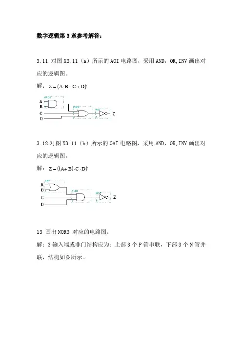
3-2 分析题图3-2所示电路,要求:写出输出逻辑函数表达式,列出真值表,画出卡诺图,并总结电路功能。
解:由题图3-2从输入信号出发,写出输出F 的逻辑函数表达式为()()F A B C D =:::将上式中的A 、 B 、C 、D 取值0000~1111,求出F ,可得真值表和卡诺图分别如题解 表3-2和题解 图3-1所示。
题解 表3-2A B C DA B : C D :F0 0 0 0 1 1 1 0 0 0 1 1 0 0 0 0 1 0 1 0 0 0 0 1 1 1 1 1 0 1 0 0 0 1 0 0 1 0 1 0 0 1 0 1 1 0 0 0 1 0 1 1 1 0 1 0 1 0 0 0 0 1 0 1 0 0 1 0 0 11 0 1 0 0 0 1 1 0 1 1 0 1 0 1 1 0 0 1 1 1 1 1 0 1 1 0 0 1 1 1 0 1 0 0 1 1 1 1 1 1 1综上,由题解 表3-2可以看出,当输入A 、 B 、C 、D 中含有偶数个“1”时,输出;否则,当输入A 、 B 、C 、D 中含有奇数个“1”时,输出。
数字逻辑第三版答案【篇一:数字逻辑第三章作业答案】txt>?z???a?b??c?d???abzc3.12?z????a?b???c?d???abzcvddabcaabcz3.20 74hc00的dcnoise marginlow state:1.35-0.33(0.1) = 1.02(1.25)vhigh state: 3.84 (4.4)-3.15=0.69 (1.25)v 括号里的数值表示输出驱动cmos负载时的直流噪声容限 3.57azbvddazz???a??b?c???【篇二:数字逻辑(第二版)毛法尧课后题答案(1-6章)】列不同进制数写成按权展开式:1.2 完成下列二进制表达式的运算:1.3 将下列二进制数转换成十进制数、八进制数和十六进制数:⑵ (0.207)10=(0.34fdf)16=(0.001101)2=(0.15176)8⑶ (33.333)10=(21.553f7)16=(100001.010101)2=(41.25237)81.5 如何判断一个二进制正整数b=b6b5b4b3b2b1b0能否被(4)10整除?解: 一个二进制正整数被(2)10除时,小数点向左移动一位, 被(4)10除时,小数点向左移动两位,能被整除时,应无余数,故当b1=0和b0=0时, 二进制正整数b=b6b5b4b3b2b1b0能否被(4)10整除.1.6 写出下列各数的原码、反码和补码:⑴ 0.1011[0.1011]原=0.1011; [0.1011]反=0.1011; [0.1011]补=0.1011⑵ 0.0000[0.000]原=0.0000; [0.0000]反=0.0000; [0.0000]补=0.0000⑶ -10110[-10110]原=110110; [-10110]反=101001; [-10110]补=1010101.7 已知[n]补=1.0110,求[n]原,[n]反和n.解:由[n]补=1.0110得: [n]反=[n]补-1=1.0101, [n]原=1.1010,n=-0.10101.8 用原码、反码和补码完成如下运算:⑴ 0000101-0011010[0000101-0011010]原=10010101;∴0000101-0011010=-0010101。
f 习题三3.1写出如图判p3.1中各逻辑图的逻辑表达式,并化简成最简与或表达式。
BCBC(a) (b)AA C(c)(d)图p3.1题3.1逻辑图解:(a )C B C B A C B C B A F +=•=(b) 1=)+(+)+(+)+(=+•+•+=C B B A C A C B B A C A F(c)CA BC AB C B A AB C B A AB F++=)⊕(+=)⊕(+=1 ABC C B A C B A C B A C B A F +++=⊕⊕=2(d)F=A⊙B⊙C= ABC C B A C B A C B A C AB B A C AB B A +++=•)+(+•+3.2、3.2、化简下列逻辑函数,并用与非门和或非门实现。
解:(1)∑)7,3,2,0(=),,(m C B A F与非门实现:BC B A BC B A F •=+=或非门实现:C B C A F +=,C B C A C B C A F F +++=)+)(+(== (2) C A C B AB C B A F ++=),,( 解:与非门实现:AB C AB C F •=+=或非门实现:C B C A F +=,C B C A C B C A F F +++=)+)(+(== ┏ (^ω^)=☞(3) ABD D C B C A B A D C B A F +++=),,,( 解:与非门实现:BCD AC AB BCD AC AB F ••=++= 或非门实现:C B D A C A B A F +++=,C BD A C A B A C B D A C A B A F F +++++++=)+)(+)(+)(+(==(4) ∑)15,14,10,8,2,0(=),,,(m D C B A F解:与非门实现:ABC BD ABC BD F •=+= 或非门实现:C B D B D A B A F +++=,C BD B D A B A C B D B D A B A F F +++++++=)+)(+)(+)(+(==(图略)3.3、分析如图p3.2所示组合逻辑电路,写出输出函数表达式,列出真值表,说明电路的逻辑功能。
C HAPTER 3 Exercise 3.1Exercise 3.3Exercise 3.5Exercise 3.7The circuit is sequential because it involves feedback and the output de-pends on previous values of the inputs. This is a SR latch. When S = 0 and R = 1, the circuit sets Q to 1. When S = 1 and R = 0, the circuit resets Q to 0. When both S and R are 1, the circuit remembers the old value. And when both S and R are 0, the circuit drives both outputs to 1.Exercise 3.9Exercise 3.11If A and B have the same value, C takes on that value. Otherwise, C retains its old value.Exercise 3.13Exercise 3.15Exercise 3.17If N is even, the circuit is stable and will not oscillate.Exercise 3.19The system has at least five bits of state to represent the 24 floors that the elevator might be on.Exercise 3.21The FSM could be factored into four independent state machines, one for each student. Each of these machines has five states and requires 3 bits, so at least 12 bits of state are required for the factored design.Exercise 3.23This finite state machine asserts the output Q when A AND B is TRUE.10S000S101S210TABLE 3.1State encoding for Exercise 3.231010000X000001X01001X000001X11001011101100000010010001010000 TABLE 3.2Combined state transition and output table with binary encodings for Exercise 3.23=S'1S1S0B S1AB+=S'0S1S0A=Q'S1ABExercise 3.25s t a t e e n c o d i n gs1:0S0000S1001TABLE 3.3State encoding for Exercise 3.2510S2010S3100S4101TABLE 3.3State encoding for Exercise 3.2521021000000000 00010010 00100000 00110100 01001000 01011010 10000000 10010011 10101001 10111010 TABLE 3.4Combined state transition and output table with binary encodings for Exercise 3.25=S'2S2S1S0S2S1S0+=S'1S2S1S0A=()+S'0A S2S0S2S1=Q S2S1S0A S2S1S0A+Exercise 3.27FIGURE 3.12020000001001011011010010110110111111101101100100000TABLE 3.5State transition table for Exercise 3.27S '2S 1S 0S 2S 0+=S '1S 2S 0S 1S 0+=S '0S 2S 1 =Q 2S 2=Q 1S 1=Q 0S 0=FIGURE 3.2Hardware for Gray code counter FSM for Exercise 3.27Exercise 3.29(a)FIGURE 3.3Waveform showing Z output for Exercise 3.29(b) This FSM is a Mealy FSM because the output depends on the current value of the input as well as the current state.(c)FIGURE 3.4State transition diagram for Exercise 3.29(Note: another viable solution would be to allow the state to transition from S0 to S1 on . The arrow from S0 to S0 would then be .)BA 0/BA 0/c u r r e n t s t a t es 1:0i n p u t s n e x t s t a t es '1:0o u t p u tz b a 00X 0000000111000110110100000010111101101010111011100X 00010110TABLE 3.6State transition table for Exercise 3.29FIGURE 3.5Hardware for FSM of Exercise 3.26Note: One could also build this functionality by registering input A , pro-ducing both the logical AND and OR of input A and its previous (registered)101101111000001101111111010111110111010TABLE 3.6State transition table for Exercise 3.29S '1BA S 1S 0+()BA S 1S 0+()+=S '0A S 1S 0B ++()=Z BA S 0A B +()+=value, and then muxing the two operations using B. The output of the mux is Z: Z = AA prev (if B = 0); Z = A + A prev (if B = 1).Exercise 3.31This finite state machine is a divide-by-two counter (see Section 3.4.2) when X = 0. When X = 1, the output, Q, is HIGH.1010000010011101000011101X X01TABLE 3.7State transition table with binary encodings for Exercise 3.31100000111X1TABLE 3.8Output table for Exercise 3.31Exercise 3.33(a) First, we calculate the propagation delay through the combinational log-ic:t pd = 3t pd_XOR= 3 × 100 ps= 300 psNext, we calculate the cycle time:T c≥ t pcq + t pd + t setup≥[70 + 300 + 60] ps= 430 psf = 1 / 430 ps = 2.33 GHz(b)T c > t pcq + t pd + t setup + t skewThus,t skew < T c - (t pcq + t pd + t setup), where T c = 1 / 2 GHz = 500 ps <[500 - 430] ps = 70 ps(c)First, we calculate the contamination delay through the combinational log-ic:t cd = t cd_XOR= 55 pst ccq + t cd > t hold + t skewThus,t skew < (t ccq + t cd) - t hold< (50 + 55) - 20< 85 ps(d)FIGURE 3.6Alyssa’s improved circuit for Exercise 3.33First, we calculate the propagation and contamination delays through the combinational logic:t pd = 2t pd_XOR= 2 × 100 ps= 200 pst cd = 2t cd_XOR= 2 × 55 ps= 110 psNext, we calculate the cycle time:T c≥ t pcq + t pd + t setup≥[70 + 200 + 60] ps= 330 psf = 1 / 330 ps = 3.03 GHzt skew < (t ccq + t cd) - t hold< (50 + 110) - 20< 140 psExercise 3.35(a) T c= 1 / 40 MHz = 25 nsT c ≥ t pcq + Nt CLB + t setup25 ns≥[0.72 + N(0.61) + 0.53] psThus, N < 38.9N = 38(b)t skew < (t ccq + t cd_CLB ) - t hold < [(0.5 + 0.3) - 0] ns < 0.8 ns = 800 psExercise 3.37P(failure)/sec = 1/MTBF = 1/(50 years * 3.15 x 10⁷ sec/year) = 6.34 x 10⁻¹⁰ (EQ 3.26)P(failure)/sec waiting for one clock cycle: N*(T 0/T c )*e -(Tc-tsetup)/Tau = 0.5 * (110/1000) * e -(1000-70)/100 = 5.0 x 10⁻⁶P(failure)/sec waiting for two clock cycles: N*(T 0/T c )*[e -(Tc-tsetup)/Tau ]2 = 0.5 * (110/1000) * [e-(1000-70)/100]2 = 4.6 x 10⁻¹⁰This is just less than the required probability of failure (6.34 x10⁻¹⁰). Thus, 2 cycles of waiting is just adequate to meet the MTBF.Exercise 3.39We assume a two flip-flop synchronizer. The most significant impact on the probability of failure comes from the exponential component. If we ignore the T 0/T c term in the probability of failure equation, assuming it changes little with increases in cycle time, we get:Solving for T c 2 - T c 1, we get:P failure ()et τ--–=MTBF 1P failure ()--------------------------eT c t setup –τ-----------------------==MTBF 2MTBF 1------------------10e T c 2T c 1–30ps ---------------------==T c 2T c 1–69ps=Thus, the clock cycle time must increase by 69 ps. This holds true for cycle times much larger than T0 (20 ps) and the increased time (69 ps).Question 3.15050000001000001000000110000010000100000010000010100010000010000010000001001000001001000000001000100010100000100000100000010000100000110000000000101000001000001TABLE 3.9State transition table for Question 3.1 =S'5S4A=S'4S3A=S'3S2A=S'2S1A=()++S'1A S1S3S5=()+++S'0A S0S2S4S5=Q S5FIGURE 3.8Finite state machine hardware for Question 3.1Question 3.3A latch allows input D to flow through to the output Q when the clock is HIGH. A flip-flop allows input D to flow through to the output Q at the clock edge. A flip-flop is preferable in systems with a single clock. Latches are pref-erable in two-phase clocking systems, with two clocks. The two clocks are used to eliminate system failure due to hold time violations. Both the phase and fre-quency of each clock can be modified independently.Question 3.5FIGURE 3.9State transition diagram for edge detector circuit of Question 3.5n te 10i n p u t n e x t s t a t es'1:0a000000010101000011101000010110TABLE 3.10State transition table for Question 3.5 S'1AS1=S'0AS1S0=S O L U T I O N S 61David Money Harris and Sarah L. Harris, Digital Design and Computer Architecture, 2nd Edition © 2012 by Elsevier Inc.Exercise SolutionsFIGURE 3.10Finite state machine hardware for Question 3.5Question 3.7A flip-flop with a negative hold time allows D to start changing before the clock edge arrives.Question 3.9Without the added buffer, the propagation delay through the logic, t pd , mustbe less than or equal to T c - (t pcq + t setup ). However, if you add a buffer to theclock input of the receiver, the clock arrives at the receiver later. The earliestthat the clock edge arrives at the receiver is t cd_BUF after the actual clock edge.Thus, the propagation delay through the logic is now given an extra t cd _BUF . So,t pd now must be less than T c + t cd _BUF - (t pcq + t setup ).Q S 1=David Money Harris and Sarah L. Harris, Digital Design and Computer Architecture, © 2007 by Elsevier Inc. Exercise Solutions62S O L U T I O N S c h a p t e r3。