半导体集成电路原理与设计—第三章答辩
- 格式:ppt
- 大小:803.50 KB
- 文档页数:25
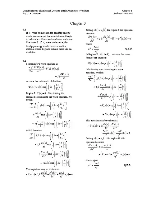
Chapter 33.1If o a were to increase, the bandgap energy would decrease and the material would begin to behave less like a semiconductor and more like a metal. If o a were to decrease, the bandgap energy would increase and thematerial would begin to behave more like an insulator._______________________________________ 3.2Schrodinger's wave equation is:()()()t x x V xt x m ,,2222ψ⋅+∂ψ∂- ()tt x j ∂ψ∂=, Assume the solution is of the form:()()⎥⎥⎦⎤⎢⎢⎣⎡⎪⎪⎭⎫ ⎝⎛⎪⎭⎫ ⎝⎛-=ψt E kx j x u t x exp , Region I: ()0=x V . Substituting theassumed solution into the wave equation, we obtain:()⎥⎥⎦⎤⎢⎢⎣⎡⎪⎪⎭⎫ ⎝⎛⎪⎭⎫ ⎝⎛-⎩⎨⎧∂∂-t E kx j x jku x m exp 22 ()⎪⎭⎪⎬⎫⎥⎥⎦⎤⎢⎢⎣⎡⎪⎪⎭⎫ ⎝⎛⎪⎭⎫ ⎝⎛-∂∂+t E kx j x x u exp ()⎥⎥⎦⎤⎢⎢⎣⎡⎪⎪⎭⎫ ⎝⎛⎪⎭⎫ ⎝⎛-⋅⎪⎭⎫ ⎝⎛-=t E kx j x u jE j exp which becomes()()⎥⎥⎦⎤⎢⎢⎣⎡⎪⎪⎭⎫ ⎝⎛⎪⎭⎫ ⎝⎛-⎩⎨⎧-t E kx j x u jk m exp 222 ()⎥⎥⎦⎤⎢⎢⎣⎡⎪⎪⎭⎫ ⎝⎛⎪⎭⎫ ⎝⎛-∂∂+t E kx j x x u jkexp 2 ()⎪⎭⎪⎬⎫⎥⎥⎦⎤⎢⎢⎣⎡⎪⎪⎭⎫ ⎝⎛⎪⎭⎫ ⎝⎛-∂∂+t E kx j x x u exp 22 ()⎥⎥⎦⎤⎢⎢⎣⎡⎪⎪⎭⎫ ⎝⎛⎪⎭⎫ ⎝⎛-+=t E kx j x Eu exp This equation may be written as()()()()0222222=+∂∂+∂∂+-x u mE x x u x x u jk x u kSetting ()()x u x u 1= for region I, the equation becomes:()()()()021221212=--+x u k dx x du jk dxx u d α where222mE=α Q.E.D.In Region II, ()O V x V =. Assume the same form of the solution:()()⎥⎥⎦⎤⎢⎢⎣⎡⎪⎪⎭⎫ ⎝⎛⎪⎭⎫ ⎝⎛-=ψt E kx j x u t x exp , Substituting into Schrodinger's wave equation, we find:()()⎥⎥⎦⎤⎢⎢⎣⎡⎪⎪⎭⎫ ⎝⎛⎪⎭⎫ ⎝⎛-⎩⎨⎧-t E kx j x u jk m exp 222 ()⎥⎥⎦⎤⎢⎢⎣⎡⎪⎪⎭⎫ ⎝⎛⎪⎭⎫ ⎝⎛-∂∂+t E kx j x x u jkexp 2 ()⎪⎭⎪⎬⎫⎥⎥⎦⎤⎢⎢⎣⎡⎪⎪⎭⎫ ⎝⎛⎪⎭⎫ ⎝⎛-∂∂+t E kx j x x u exp 22 ()⎥⎥⎦⎤⎢⎢⎣⎡⎪⎪⎭⎫ ⎝⎛⎪⎭⎫ ⎝⎛-+t E kx j x u V O exp ()⎥⎥⎦⎤⎢⎢⎣⎡⎪⎪⎭⎫ ⎝⎛⎪⎭⎫ ⎝⎛-=t E kx j x Eu exp This equation can be written as:()()()2222x x u x x u jk x u k ∂∂+∂∂+- ()()02222=+-x u mEx u mV OSetting ()()x u x u 2= for region II, this equation becomes()()dx x du jk dxx u d 22222+ ()022222=⎪⎪⎭⎫ ⎝⎛+--x u mV k O α where again222mE=α Q.E.D._______________________________________3.3We have ()()()()021221212=--+x u k dx x du jk dx x u d α Assume the solution is of the form:()()[]x k j A x u -=αexp 1 ()[]x k j B +-+αexpThe first derivative is()()()[]x k j A k j dxx du --=ααexp 1()()[]x k j B k j +-+-ααexp and the second derivative becomes()()[]()[]xk j A k j dx x u d --=ααexp 2212 ()[]()[]x k j B k j +-++ααexp 2Substituting these equations into thedifferential equation, we find ()()[]x k j A k ---ααexp 2()()[]x k j B k +-+-ααexp 2(){()[]x k j A k j jk --+ααexp 2()()[]}x k j B k j +-+-ααexp ()()[]{x k j A k ---ααexp 22 ()[]}0exp =+-+x k j B α Combining terms, we obtain()()()[]222222αααα----+--k k k k k ()[]x k j A -⨯αexp()()()[]222222αααα--++++-+k k k k k ()[]0exp =+-⨯x k j B α We find that00= Q.E.D. For the differential equation in ()x u 2 and the proposed solution, the procedure is exactly the same as above._______________________________________ 3.4We have the solutions ()()[]x k j A x u -=αexp 1()[]x k j B +-+αexp for a x <<0 and()()[]x k j C x u -=βexp 2()[]x k j D +-+βexp for 0<<-x b .The first boundary condition is ()()0021u u =which yields 0=--+D C B AThe second boundary condition is 0201===x x dx du dx duwhich yields()()()C k B k A k --+--βαα ()0=++D k β The third boundary condition is ()()b u a u -=21 which yields()[]()[]a k j B a k j A +-+-ααexp exp ()()[]b k j C --=βexp ()()[]b k j D -+-+βexp and can be written as ()[]()[]a k j B a k j A +-+-ααexp exp ()[]b k j C ---βexp()[]0exp =+-b k j D βThe fourth boundary condition isbx a x dx dudx du -===21 which yields()()[]a k j A k j --ααexp()()[]a k j B k j +-+-ααexp ()()()[]b k j C k j ---=ββexp()()()[]b k j D k j -+-+-ββexp and can be written as ()()[]a k j A k --ααexp()()[]a k j B k +-+-ααexp()()[]b k j C k ----ββexp()()[]0exp =+++b k j D k ββ_______________________________________ 3.5(b) (i) First point: πα=aSecond point: By trial and error, πα729.1=a (ii) First point: πα2=aSecond point: By trial and error, πα617.2=a_______________________________________3.6 (b) (i) First point: πα=a Second point: By trial and error,πα515.1=a (ii) First point: πα2=aSecond point: By trial and error, πα375.2=a_______________________________________ 3.7 ka a a a P cos cos sin =+'ααα Let y ka =, x a =αThen y x x x P cos cos sin =+' Consider dy d of this function.()[]{}y x x x P dy d sin cos sin 1-=+⋅'- We find()()()⎭⎬⎫⎩⎨⎧⋅+⋅-'--dy dx x x dy dx x x P cos sin 112y dydxx sin sin -=- Theny x x x x x P dy dx sin sin cos sin 12-=⎭⎬⎫⎩⎨⎧-⎥⎦⎤⎢⎣⎡+-'For πn ka y ==, ...,2,1,0=n 0sin =⇒y So that, in general,()()dk d ka d a d dy dxαα===0 And 22 mE=α Sodk dEm mE dk d ⎪⎭⎫ ⎝⎛⎪⎭⎫ ⎝⎛=-22/122221 α This implies thatdk dE dk d ==0α for an k π= _______________________________________ 3.8 (a) πα=a 1 π=⋅a E m o 212 ()()()()2103123422221102.41011.9210054.12---⨯⨯⨯==ππa m E o 19104114.3-⨯=J From Problem 3.5πα729.12=a π729.1222=⋅a E m o ()()()()2103123422102.41011.9210054.1729.1---⨯⨯⨯=πE 18100198.1-⨯=J 12E E E -=∆1918104114.3100198.1--⨯-⨯=19107868.6-⨯=Jor 24.4106.1107868.61919=⨯⨯=∆--E eV(b) πα23=aπ2223=⋅a E m o()()()()2103123423102.41011.9210054.12---⨯⨯⨯=πE18103646.1-⨯=J From Problem 3.5, πα617.24=aπ617.2224=⋅a E m o()()()()2103123424102.41011.9210054.1617.2---⨯⨯⨯=πE18103364.2-⨯=J 34E E E -=∆1818103646.1103364.2--⨯-⨯= 1910718.9-⨯=Jor 07.6106.110718.91919=⨯⨯=∆--E eV_______________________________________3.9 (a) At π=ka , πα=a 1π=⋅a E m o 212()()()()2103123421102.41011.9210054.1---⨯⨯⨯=πE19104114.3-⨯=JAt 0=ka , By trial and error, πα859.0=a o ()()()()210312342102.41011.9210054.1859.0---⨯⨯⨯=πoE19105172.2-⨯=J o E E E -=∆11919105172.2104114.3--⨯-⨯= 2010942.8-⨯=Jor 559.0106.110942.81920=⨯⨯=∆--E eV (b) At π2=ka , πα23=aπ2223=⋅a E m o()()()()2103123423102.41011.9210054.12---⨯⨯⨯=πE18103646.1-⨯=JAt π=ka . From Problem 3.5, πα729.12=aπ729.1222=⋅a E m o()()()()2103123422102.41011.9210054.1729.1---⨯⨯⨯=πE18100198.1-⨯=J23E E E -=∆1818100198.1103646.1--⨯-⨯= 19104474.3-⨯=Jor 15.2106.1104474.31919=⨯⨯=∆--E eV_______________________________________3.10 (a) πα=a 1π=⋅a E m o 212()()()()2103123421102.41011.9210054.1---⨯⨯⨯=πE19104114.3-⨯=JFrom Problem 3.6, πα515.12=aπ515.1222=⋅a E m o()()()()2103123422102.41011.9210054.1515.1---⨯⨯⨯=πE1910830.7-⨯=J 12E E E -=∆1919104114.310830.7--⨯-⨯= 19104186.4-⨯=Jor 76.2106.1104186.41919=⨯⨯=∆--E eV (b) πα23=aπ2223=⋅a E m o()()()()2103123423102.41011.9210054.12---⨯⨯⨯=πE18103646.1-⨯=JFrom Problem 3.6, πα375.24=aπ375.2224=⋅a E m o()()()()2103123424102.41011.9210054.1375.2---⨯⨯⨯=πE18109242.1-⨯=J 34E E E -=∆1818103646.1109242.1--⨯-⨯= 1910597.5-⨯=Jor 50.3106.110597.51919=⨯⨯=∆--E eV_____________________________________3.11 (a) At π=ka , πα=a 1π=⋅a E m o 212()()()()2103123421102.41011.9210054.1---⨯⨯⨯=πE19104114.3-⨯=JAt 0=ka , By trial and error, πα727.0=a oπ727.022=⋅a E m o o()()()()210312342102.41011.9210054.1727.0---⨯⨯⨯=πo E19108030.1-⨯=Jo E E E -=∆11919108030.1104114.3--⨯-⨯= 19106084.1-⨯=Jor 005.1106.1106084.11919=⨯⨯=∆--E eV (b) At π2=ka , πα23=aπ2223=⋅a E m o()()()()2103123423102.41011.9210054.12---⨯⨯⨯=πE18103646.1-⨯=JAt π=ka , From Problem 3.6,πα515.12=aπ515.1222=⋅a E m o()()()()2103423422102.41011.9210054.1515.1---⨯⨯⨯=πE1910830.7-⨯=J23E E E -=∆191810830.7103646.1--⨯-⨯= 1910816.5-⨯=Jor 635.3106.110816.51919=⨯⨯=∆--E eV_______________________________________3.12For 100=T K, ()()⇒+⨯-=-1006361001073.4170.124gE164.1=g E eV200=T K, 147.1=g E eV 300=T K, 125.1=g E eV 400=T K, 097.1=g E eV 500=T K, 066.1=g E eV 600=T K, 032.1=g E eV_______________________________________3.13The effective mass is given by1222*1-⎪⎪⎭⎫⎝⎛⋅=dk E d mWe have()()B curve dkE d A curve dk E d 2222> so that ()()B curve m A curve m **<_______________________________________ 3.14The effective mass for a hole is given by1222*1-⎪⎪⎭⎫ ⎝⎛⋅=dk E d m p We have that()()B curve dkEd A curve dk E d 2222> so that ()()B curve m A curve m p p **<_______________________________________ 3.15Points A,B: ⇒<0dk dEvelocity in -x directionPoints C,D: ⇒>0dk dEvelocity in +x directionPoints A,D: ⇒<022dk Ednegative effective massPoints B,C: ⇒>022dkEd positive effective mass _______________________________________3.16 For A: 2k C E i = At 101008.0+⨯=k m 1-, 05.0=E eV Or ()()2119108106.105.0--⨯=⨯=E J So ()2101211008.0108⨯=⨯-C3811025.1-⨯=⇒CNow ()()38234121025.1210054.12--*⨯⨯==C m 311044.4-⨯=kgor o m m ⋅⨯⨯=--*31311011.9104437.4o m m 488.0=* For B: 2k C E i =At 101008.0+⨯=k m 1-, 5.0=E eV Or ()()2019108106.15.0--⨯=⨯=E JSo ()2101201008.0108⨯=⨯-C 3711025.1-⨯=⇒CNow ()()37234121025.1210054.12--*⨯⨯==C m 321044.4-⨯=kg or o m m ⋅⨯⨯=--*31321011.9104437.4o m m 0488.0=*_______________________________________ 3.17For A: 22k C E E -=-υ()()()2102191008.0106.1025.0⨯-=⨯--C 3921025.6-⨯=⇒C()()39234221025.6210054.12--*⨯⨯-=-=C m31108873.8-⨯-=kgor o m m ⋅⨯⨯-=--*31311011.9108873.8o m m 976.0--=* For B: 22k C E E -=-υ()()()2102191008.0106.13.0⨯-=⨯--C 382105.7-⨯=⇒C()()3823422105.7210054.12--*⨯⨯-=-=C m3210406.7-⨯-=kgor o m m ⋅⨯⨯-=--*31321011.910406.7o m m 0813.0-=*_______________________________________ 3.18(a) (i) νh E =or ()()341910625.6106.142.1--⨯⨯==h E ν1410429.3⨯=Hz(ii) 141010429.3103⨯⨯===νλc E hc 51075.8-⨯=cm 875=nm(b) (i) ()()341910625.6106.112.1--⨯⨯==h E ν1410705.2⨯=Hz(ii) 141010705.2103⨯⨯==νλc410109.1-⨯=cm 1109=nm_______________________________________ 3.19(c) Curve A: Effective mass is a constantCurve B: Effective mass is positive around 0=k , and is negativearound 2π±=k ._______________________________________ 3.20()[]O O k k E E E --=αcos 1 Then()()()[]O k k E dkdE ---=ααsin 1()[]O k k E -+=ααsin 1 and()[]O k k E dk E d -=ααcos 2122Then 221222*11 αE dk E d m o k k =⋅== or 212*αE m = _______________________________________ 3.21(a) ()[]3/123/24l t dn m m m =* ()()[]3/123/264.1082.04o o m m = o dn m m 56.0=*(b) oo l t cn m m m m m 64.11082.02123+=+=* oo m m 6098.039.24+= o cn m m 12.0=*_______________________________________3.22(a) ()()[]3/22/32/3lh hh dp m m m +=*()()[]3/22/32/3082.045.0o o m m += []om ⋅+=3/202348.030187.0o dp m m 473.0=*(b) ()()()()2/12/12/32/3lh hh lh hh cpm m m m m ++=*()()()()om ⋅++=2/12/12/32/3082.045.0082.045.0 o cp m m 34.0=*_______________________________________ 3.23For the 3-dimensional infinite potential well, ()0=x V when a x <<0, a y <<0, and a z <<0. In this region, the wave equation is:()()()222222,,,,,,z z y x y z y x x z y x ∂∂+∂∂+∂∂ψψψ()0,,22=+z y x mEψ Use separation of variables technique, so let ()()()()z Z y Y x X z y x =,,ψSubstituting into the wave equation, we have222222z ZXY y Y XZ x X YZ ∂∂+∂∂+∂∂ 022=⋅+XYZ mEDividing by XYZ , we obtain 021*********=+∂∂⋅+∂∂⋅+∂∂⋅ mEz Z Z y Y Y x X XLet 01222222=+∂∂⇒-=∂∂⋅X k x X k x X X x x The solution is of the form:()x k B x k A x X x x cos sin += Since ()0,,=z y x ψ at 0=x , then ()00=X so that 0=B . Also, ()0,,=z y x ψ at a x =, so that()0=a X . Then πx x n a k = where ...,3,2,1=x nSimilarly, we have 2221y k y Y Y -=∂∂⋅ and 2221z k z Z Z -=∂∂⋅ From the boundary conditions, we find πy y n a k = and πz z n a k =where...,3,2,1=y n and ...,3,2,1=z n From the wave equation, we can write022222=+---mE k k k z y xThe energy can be written as()222222⎪⎭⎫⎝⎛++==a n n n m E E z y x n n n z y x π _______________________________________ 3.24The total number of quantum states in the 3-dimensional potential well is given (in k-space) by()332a dk k dk k g T ⋅=ππ where222 mEk =We can then writemEk 2=Taking the differential, we obtaindE E mdE E m dk ⋅⋅=⋅⋅⋅⋅=2112121 Substituting these expressions into the density of states function, we have()dE E mmE a dE E g T ⋅⋅⋅⎪⎭⎫ ⎝⎛=212233 ππ Noting that π2h = this density of states function can be simplified and written as ()()dE E m hadE E g T ⋅⋅=2/33324π Dividing by 3a will yield the density of states so that()()E hm E g ⋅=32/324π _______________________________________ 3.25 For a one-dimensional infinite potential well, 222222k a n E m n ==*πDistance between quantum states()()aa n a n k k n n πππ=⎪⎭⎫ ⎝⎛=⎪⎭⎫ ⎝⎛+=-+11 Now()⎪⎭⎫ ⎝⎛⋅=a dk dk k g T π2NowE m k n *⋅=21dE Em dk n⋅⋅⋅=*2211 Then()dE Em a dE E g n T ⋅⋅⋅=*2212 π Divide by the "volume" a , so()Em E g n *⋅=21πSo ()()()()()E E g 31341011.9067.0210054.11--⨯⋅⨯=π ()E E g 1810055.1⨯= m 3-J 1- _______________________________________3.26(a) Silicon, o n m m 08.1=*()()c n c E E h m E g -=*32/324π ()dE E E h m g kT E E c n c c c⋅-=⎰+*232/324π()()kT E E c n c c E E h m 22/332/33224+*-⋅⋅=π ()()2/332/323224kT h m n ⋅⋅=*π ()()[]()()2/33342/33123210625.61011.908.124kT ⋅⋅⨯⨯=--π ()()2/355210953.7kT ⨯=(i) At 300=T K, 0259.0=kT eV()()19106.10259.0-⨯=2110144.4-⨯=J Then ()()[]2/3215510144.4210953.7-⨯⨯=c g25100.6⨯=m 3- or 19100.6⨯=c g cm 3-(ii) At 400=T K, ()⎪⎭⎫⎝⎛=3004000259.0kT 034533.0=eV ()()19106.1034533.0-⨯=21105253.5-⨯=J Then ()()[]2/32155105253.5210953.7-⨯⨯=c g 2510239.9⨯=m 3- or 191024.9⨯=c g cm 3-(b) GaAs, o nm m 067.0=*()()[]()()2/33342/33123210625.61011.9067.024kT g c ⋅⋅⨯⨯=--π ()()2/3542102288.1kT ⨯=(i) At 300=T K, 2110144.4-⨯=kT J ()()[]2/3215410144.42102288.1-⨯⨯=c g2310272.9⨯=m 3- or 171027.9⨯=c g cm 3-(ii) At 400=T K, 21105253.5-⨯=kT J ()()[]2/32154105253.52102288.1-⨯⨯=c g2410427.1⨯=m 3-181043.1⨯=c g cm 3-_______________________________________ 3.27(a) Silicon, o p m m 56.0=* ()()E E h mE g p-=*υυπ32/324()dE E E h mg E kTE p⋅-=⎰-*υυυυπ332/324()()υυυπE kTE pE E hm 32/332/33224-*-⎪⎭⎫ ⎝⎛-=()()[]2/332/333224kT hmp-⎪⎭⎫ ⎝⎛-=*π ()()[]()()2/33342/33133210625.61011.956.024kT ⎪⎭⎫ ⎝⎛⨯⨯=--π ()()2/355310969.2kT ⨯=(i)At 300=T K, 2110144.4-⨯=kT J ()()[]2/3215510144.4310969.2-⨯⨯=υg2510116.4⨯=m3-or 191012.4⨯=υg cm 3- (ii)At 400=T K, 21105253.5-⨯=kT J()()[]2/32155105253.5310969.2-⨯⨯=υg2510337.6⨯=m3-or 191034.6⨯=υg cm 3- (b) GaAs, o p m m 48.0=*()()[]()()2/33342/33133210625.61011.948.024kT g ⎪⎭⎫ ⎝⎛⨯⨯=--πυ ()()2/3553103564.2kT ⨯=(i)At 300=T K, 2110144.4-⨯=kT J()()[]2/3215510144.43103564.2-⨯⨯=υg2510266.3⨯=m 3- or 191027.3⨯=υg cm 3-(ii)At 400=T K, 21105253.5-⨯=kT J()()[]2/32155105253.53103564.2-⨯⨯=υg2510029.5⨯=m 3-or 191003.5⨯=υg cm 3-_______________________________________ 3.28(a) ()()c nc E E h m E g -=*32/324π()()[]()c E E -⨯⨯=--3342/33110625.61011.908.124πc E E -⨯=56101929.1 For c E E =; 0=c g1.0+=c E E eV; 4610509.1⨯=c g m 3-J 1-2.0+=c E E eV; 4610134.2⨯=m 3-J 1-3.0+=c E E eV; 4610614.2⨯=m 3-J 1- 4.0+=c E E eV; 4610018.3⨯=m 3-J 1- (b) ()E E h m g p-=*υυπ32/324()()[]()E E -⨯⨯=--υπ3342/33110625.61011.956.024E E -⨯=υ55104541.4 For υE E =; 0=υg1.0-=υE E eV; 4510634.5⨯=υg m 3-J 1-2.0-=υE E eV; 4510968.7⨯=m 3-J 1-3.0-=υE E eV; 4510758.9⨯=m 3-J 1-4.0-=υE E eV; 4610127.1⨯=m 3-J 1-_______________________________________ 3.29(a) ()()68.256.008.12/32/32/3=⎪⎭⎫ ⎝⎛==**pnc m m g g υ(b) ()()0521.048.0067.02/32/32/3=⎪⎭⎫ ⎝⎛==**pncmm g g υ_______________________________________3.30 Plot _______________________________________3.31(a) ()()()!710!7!10!!!-=-=i i i i i N g N g W()()()()()()()()()()()()1201238910!3!7!78910===(b) (i) ()()()()()()()()12!10!101112!1012!10!12=-=i W 66=(ii) ()()()()()()()()()()()()1234!8!89101112!812!8!12=-=i W 495=_______________________________________ 3.32 ()⎪⎪⎭⎫⎝⎛-+=kT E E E f F exp 11(a) kT E E F =-, ()()⇒+=1exp 11E f ()269.0=E f (b) kT E E F 5=-, ()()⇒+=5exp 11E f()31069.6-⨯=E f(c) kT E E F 10=-, ()()⇒+=10exp 11E f ()51054.4-⨯=E f_______________________________________ 3.33()⎪⎪⎭⎫ ⎝⎛-+-=-kT E E E f F exp 1111or()⎪⎪⎭⎫ ⎝⎛-+=-kT E E E f F exp 111(a) kT E E F =-, ()269.01=-E f (b) kT E E F 5=-, ()31069.61-⨯=-E f(c) kT E E F 10=-, ()51054.41-⨯=-E f_______________________________________3.34 (a) ()⎥⎦⎤⎢⎣⎡--≅kT E E f F F exp c E E =; 61032.90259.030.0exp -⨯=⎥⎦⎤⎢⎣⎡-=F f 2kT E c +; ()⎥⎦⎤⎢⎣⎡+-=0259.020259.030.0exp F f 61066.5-⨯=kT E c +; ()⎥⎦⎤⎢⎣⎡+-=0259.00259.030.0exp F f 61043.3-⨯=23kT E c +; ()()⎥⎦⎤⎢⎣⎡+-=0259.020259.0330.0exp F f 61008.2-⨯= kT E c 2+; ()()⎥⎦⎤⎢⎣⎡+-=0259.00259.0230.0exp F f 61026.1-⨯= (b) ⎥⎦⎤⎢⎣⎡-+-=-kT E E f F F exp 1111 ()⎥⎦⎤⎢⎣⎡--≅kT E E F exp υE E =; ⎥⎦⎤⎢⎣⎡-=-0259.025.0exp 1F f 51043.6-⨯= 2kT E -υ; ()⎥⎦⎤⎢⎣⎡+-=-0259.020259.025.0exp 1F f 51090.3-⨯=kT E -υ; ()⎥⎦⎤⎢⎣⎡+-=-0259.00259.025.0exp 1F f 51036.2-⨯=23kTE -υ; ()()⎥⎦⎤⎢⎣⎡+-=-0259.020259.0325.0exp 1F f 51043.1-⨯= kT E 2-υ;()()⎥⎦⎤⎢⎣⎡+-=-0259.00259.0225.0exp 1F f 61070.8-⨯=_______________________________________3.35 ()()⎥⎦⎤⎢⎣⎡-+-=⎥⎦⎤⎢⎣⎡--=kT E kT E kT E E f F c F F exp exp and()⎥⎦⎤⎢⎣⎡--=-kT E E f F F exp 1 ()()⎥⎦⎤⎢⎣⎡---=kT kT E E F υexp So ()⎥⎦⎤⎢⎣⎡-+-kT E kT E F c exp ()⎥⎦⎤⎢⎣⎡+--=kT kT E E F υexp Then kT E E E kT E F F c +-=-+υ Or midgap c F E E E E =+=2υ_______________________________________ 3.3622222ma n E n π= For 6=n , Filled state()()()()()2103122234610121011.92610054.1---⨯⨯⨯=πE 18105044.1-⨯=Jor 40.9106.1105044.119186=⨯⨯=--E eV For 7=n , Empty state()()()()()2103122234710121011.92710054.1---⨯⨯⨯=πE 1810048.2-⨯=Jor 8.12106.110048.219187=⨯⨯=--E eV Therefore 8.1240.9<<F E eV_______________________________________ 3.37(a) For a 3-D infinite potential well()222222⎪⎭⎫ ⎝⎛++=a n n n mE z y x π For 5 electrons, the 5th electron occupies the quantum state 1,2,2===z y x n n n ; so()2222252⎪⎭⎫ ⎝⎛++=a n n n m E z y x π()()()()()21031222223410121011.9212210054.1---⨯⨯++⨯=π 1910761.3-⨯=J or 35.2106.110761.319195=⨯⨯=--E eV For the next quantum state, which is empty,the quantum state is 2,2,1===z y x n n n . This quantum state is at the same energy, so35.2=F E eV(b) For 13 electrons, the 13th electron occupies the quantum state3,2,3===z y x n n n ; so ()()()()()2103122222341310121011.9232310054.1---⨯⨯++⨯=πE1910194.9-⨯=Jor 746.5106.110194.9191913=⨯⨯=--E eV The 14th electron would occupy the quantum state 3,3,2===z y x n n n . This state is atthe same energy, so746.5=F E eV _______________________________________ 3.38The probability of a state at E E E F ∆+=1being occupied is ()⎪⎭⎫ ⎝⎛∆+=⎪⎪⎭⎫ ⎝⎛-+=kT E kT E E E f F exp 11exp 11111 The probability of a state at E E E F∆-=2being empty is()⎪⎪⎭⎫ ⎝⎛-+-=-kT E E E f F 222exp 1111⎪⎭⎫ ⎝⎛∆-+⎪⎭⎫ ⎝⎛∆-=⎪⎭⎫ ⎝⎛∆-+-=kT E kT E kT E exp 1exp exp 111or()⎪⎭⎫ ⎝⎛∆+=-kT E E f exp 11122so ()()22111E f E f -= Q.E.D. _______________________________________3.39 (a) At energy 1E , we want 01.0exp 11exp 11exp 1111=⎪⎪⎭⎫ ⎝⎛-+⎪⎪⎭⎫ ⎝⎛-+-⎪⎪⎭⎫ ⎝⎛-kT E E kT E E kT E E F F FThis expression can be written as 01.01exp exp 111=-⎪⎪⎭⎫ ⎝⎛-⎪⎪⎭⎫⎝⎛-+kT E E kT E E F F or()⎪⎪⎭⎫ ⎝⎛-=kT E E F 1exp 01.01 Then()100ln 1kT E E F += or kT E E F 6.41+= (b) At kT E E F 6.4+=, ()()6.4exp 11exp 1111+=⎪⎪⎭⎫ ⎝⎛-+=kT E E E f F which yields()01.000990.01≅=E f _______________________________________3.40(a)()()⎥⎦⎤⎢⎣⎡--=⎥⎦⎤⎢⎣⎡--=0259.050.580.5exp exp kT E E f F F 61032.9-⨯= (b) ()060433.03007000259.0=⎪⎭⎫⎝⎛=kT eV 31098.6060433.030.0exp -⨯=⎥⎦⎤⎢⎣⎡-=F f(c) ()⎥⎦⎤⎢⎣⎡--≅-kT E E f F F exp 1 ⎥⎦⎤⎢⎣⎡-=kT 25.0exp 02.0 or 5002.0125.0exp ==⎥⎦⎤⎢⎣⎡+kT ()50ln 25.0=kT or ()()⎪⎭⎫⎝⎛===3000259.0063906.050ln 25.0T kTwhich yields 740=T K _______________________________________3.41 (a) ()00304.00259.00.715.7exp 11=⎪⎭⎫⎝⎛-+=E f or 0.304% (b) At 1000=T K, 08633.0=kT eVThen ()1496.008633.00.715.7exp 11=⎪⎭⎫⎝⎛-+=E for 14.96% (c) ()997.00259.00.785.6exp 11=⎪⎭⎫ ⎝⎛-+=E for 99.7% (d) At F E E =, ()21=E f for all temperatures _______________________________________ 3.42 (a) For 1E E = ()()⎥⎦⎤⎢⎣⎡--≅⎪⎪⎭⎫ ⎝⎛-+=kT E E kT E E E f F F 11exp exp 11Then ()611032.90259.030.0exp -⨯=⎪⎭⎫ ⎝⎛-=E f For 2E E =, 82.030.012.12=-=-E E F eVThen ()⎪⎭⎫ ⎝⎛-+-=-0259.082.0exp 1111E for()⎥⎦⎤⎢⎣⎡⎪⎭⎫ ⎝⎛---≅-0259.082.0exp 111E f 141078.10259.082.0exp -⨯=⎪⎭⎫ ⎝⎛-=(b) For 4.02=-E E F eV,72.01=-F E E eV At 1E E =,()()⎪⎭⎫⎝⎛-=⎥⎦⎤⎢⎣⎡--=0259.072.0exp exp 1kT E E E f F or()131045.8-⨯=E f At 2E E =,()()⎥⎦⎤⎢⎣⎡--=-kT E E E f F 2exp 1 ⎪⎭⎫ ⎝⎛-=0259.04.0expor()71096.11-⨯=-E f_______________________________________ 3.43(a) At 1E E =()()⎪⎭⎫⎝⎛-=⎥⎦⎤⎢⎣⎡--=0259.030.0exp exp 1kT E E E f F or()61032.9-⨯=E fAt 2E E =, 12.13.042.12=-=-E E F eV So()()⎥⎦⎤⎢⎣⎡--=-kT E E E f F 2exp 1 ⎪⎭⎫ ⎝⎛-=0259.012.1expor()191066.11-⨯=-E f (b) For 4.02=-E E F ,02.11=-F E E eV At 1E E =,()()⎪⎭⎫⎝⎛-=⎥⎦⎤⎢⎣⎡--=0259.002.1exp exp 1kT E E E f F or()181088.7-⨯=E f At 2E E =,()()⎥⎦⎤⎢⎣⎡--=-kT E E E f F 2exp 1 ⎪⎭⎫⎝⎛-=0259.04.0expor ()71096.11-⨯=-E f_______________________________________ 3.44()1exp 1-⎥⎦⎤⎢⎣⎡⎪⎪⎭⎫ ⎝⎛-+=kTE E E f Fso()()2exp 11-⎥⎦⎤⎢⎣⎡⎪⎪⎭⎫ ⎝⎛-+-=kT E E dE E df F⎪⎪⎭⎫ ⎝⎛-⎪⎭⎫⎝⎛⨯kT E E kT F exp 1or()2exp 1exp 1⎥⎦⎤⎢⎣⎡⎪⎪⎭⎫ ⎝⎛-+⎪⎪⎭⎫ ⎝⎛-⎪⎭⎫⎝⎛-=kT E E kT E E kT dE E df F F (a) At 0=T K, For()00exp =⇒=∞-⇒<dE dfE E F()0exp =⇒+∞=∞+⇒>dEdfE E FAt -∞=⇒=dEdfE E F(b) At 300=T K, 0259.0=kT eVFor F E E <<, 0=dE dfFor F E E >>, 0=dEdfAt F E E =,()()65.91110259.012-=+⎪⎭⎫ ⎝⎛-=dE df (eV)1-(c) At 500=T K, 04317.0=kT eVFor F E E <<, 0=dE dfFor F E E >>, 0=dE df At F E E =,()()79.511104317.012-=+⎪⎭⎫ ⎝⎛-=dE df (eV)1- _______________________________________3.45(a) At midgap E E =,()⎪⎪⎭⎫⎝⎛+=⎪⎪⎭⎫ ⎝⎛-+=kT E kT E E E f g F 2exp 11exp 11 Si: 12.1=g E eV,()()⎥⎦⎤⎢⎣⎡+=0259.0212.1exp 11E for ()101007.4-⨯=E fGe: 66.0=g E eV()()⎥⎦⎤⎢⎣⎡+=0259.0266.0exp 11E f or ()61093.2-⨯=E fGaAs: 42.1=g E eV ()()⎥⎦⎤⎢⎣⎡+=0259.0242.1exp 11E for()121024.1-⨯=E f(b) Using the results of Problem 3.38, the answers to part (b) are exactly the same as those given in part (a)._______________________________________3.46 (a) ()⎥⎦⎤⎢⎣⎡--=kT E E f F F exp ⎥⎦⎤⎢⎣⎡-=-kT 60.0exp 108 or ()810ln 60.0+=kT ()032572.010ln 60.08==kT eV ()⎪⎭⎫⎝⎛=3000259.0032572.0T so 377=T K (b) ⎥⎦⎤⎢⎣⎡-=-kT 60.0exp 106 ()610ln 60.0+=kT()043429.010ln 60.06==kT ()⎪⎭⎫ ⎝⎛=3000259.0043429.0Tor 503=T K_______________________________________3.47(a) At 200=T K, ()017267.03002000259.0=⎪⎭⎫ ⎝⎛=kT eV ⎪⎪⎭⎫ ⎝⎛-+==kT E E f F F exp 1105.019105.01exp =-=⎪⎪⎭⎫ ⎝⎛-kT E E F()()()19ln 017267.019ln ==-kT E E F 05084.0=eV By symmetry, for 95.0=F f , 05084.0-=-F E E eVThen ()1017.005084.02==∆E eV (b) 400=T K, 034533.0=kT eV For 05.0=F f , from part (a),()()()19ln 034533.019ln ==-kT E E F 10168.0=eVThen ()2034.010168.02==∆E eV _______________________________________。
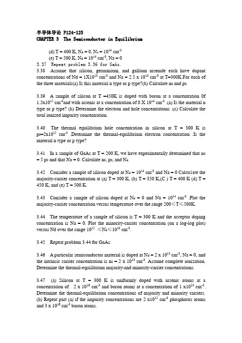
半导体导论 P124-125CHAPTER 3 The Semiconductor in Equilibrium(d) T = 400 K, N d = 0, N a = 1014 cm-3(e) T = 500 K, N d = 1014 cm-3, Na = 03.37 Repeat problem 3.36 for GaAs.3.38 Assume that silicon, germanium, and gallium arsenide each have dopant concentrations of Nd = 1X1013 cm-3 and Na = 2.5 x 1014 cm-3 at T=300K.For each of the three materials(a) Is this material n type or p type?(b) Calculate n0 and p0.3.39 A sample of silicon at T =450K is doped with boron at a concentration 0f 1.5x1015 cm-3and with arsenic at a concentration of 8 X 1014 cm-3 .(a) Is the material n type or p type? (b) Determine the electron and hole concentrations .(c) Calculate the total ionized impurity concentration.3.40 The thermal equilibrium hole concentration in silicon at T = 300 K is p0=2x1015cm-3.Determine the thermal-equilibrium electron concentration .Is the material n type or p type?3.41 In a sample of GaAs at T = 200 K, we have experimentally determined that n0 = 5 p0 and that Na = 0. Calculate n0, p0, and N d.3.42 Consider a sample of silicon doped at N d = 1014 cm-3 and Na = 0 Calcu1ate the majority-carrier concentration at (a) T = 300 K, (b) T = 350 K,(C ) T = 400 K (d) T = 450 K, and (e) T = 500 K.3.43 Consider a sample of silicon doped at N d= 0 and Na = 1014cm-3 .Plot the majority-carrier concentration versus temperature over the range 200≤T≤500K.3.44 The temperature of a sample of silicon is T = 300 K and the acceptor doping concentration is Na = 0. Plot the minority-carrier concentration (on a log-log plot) versus Nd over the range 1015≤N d≤1018 cm-3.3.45 Repeat problem 3.44 for GaAs.3.46 A particular semiconductor material is doped at N d = 2 x 1013 cm-3, Na = 0, and the intrinsic carrier concentration is ni = 2 x 1013 cm-3. Assume complete ionization. Determine the thermal-equilibrium majority-and minority-carrier concentrations.3.47 (a) Silicon at T = 300 K is uniformly doped with arsenic atoms at a concentration of 2 x 1016 cm-3 and boron atoms at a concentration of 1 x1013 cm-3. Determine the thermal-equilibrium concentrations of majority and minority carriers.(b) Repeat part (a) if the impurity concentrations are 2 x1015 cm-3 phosphorus atoms and 3 x 1016 cm-3 boron atoms.3.48 In silicon at T = 300 K, we have experimentally found that n0=4.5 x 104 cm-3and N d=5x1015cm-3. (a) Is the material n type or p type? (b) Determine the majority and minority-carrier concentrations. (c) What types and concentrations of impurity atoms exist in the material?Section 3.6 Position of Fermi Energy Level3.49 Consider germanium with an acceptor concentration of Na = 1015 cm-3 and a donor concentration of N d = 0. Consider temperatures of T = 200, 400,and 600 K. Calculate the position of the Fermi energy with respect to the intrinsic Ferrni level at these temperatures.3.50 Consider germanium at T = 300 K with donor concentrations of N d= 104, 1016and1018 cm-3 .Let Na = 0. Calculate the position of the Fermi energy level with respect to the intrinsic Fermi level for these doping concentrations.3.51 A GaAs device is doped with a donor concentration of 3X1015cm-3 .For the device to operate properly ,the intrinsic carrier concentration must remain less than 5 percent of the total electron concentration .What is the maximum temperature that the device may operate?3.52 Consider germanium with an concentration of Na=1015cm-3and a donor concentration of N d=0.Plot the position of the Fermi energy with respect to the intrinsic Fermi level as a function of temperature over the range 200 ≤T ≤600 K.3,53 Consider silicon at T =300K with Na=0. Plot the position of the Fermi energy with respect to the intrinsic Fermi level as a function of the donor doping concentration over the range 1014≤N d≤1018cm-3.3.54 For a particular semiconductor,Eg=1.50eV,m*p=10m*n,T=300K,and ni=105cm-3. (a)Determine the position of the intrinsic Fermi energy level with respect to the center of the bandgap. (b)Impurity atoms are added so that the Fermi energy level is 0.45eV below the center of the bandgap .(i)Are acceptor or donor atoms added? (ii)What is the concentration if impurity atoms added?3.55 Silicon at T = 300 K contains acceptor atoms at a concentration of Na = 5 x1015cm-3 . Donor atoms are add forming an n-type compensated semiconductor such that the Fermi level is 0.215 eV below the conduction band edge .What concentration of donor atoms are added?3.56 Silicon at T = 300 K is doped with acceptor atoms at a concentration of Na = 7 x1015cm-3. (a) Determine E f-E v. (b) Calculate the concentration of additional acceptor atoms that must be added to move the Fermi level a distance kT closer to thevalence-band edge.3.57 (a) Determine the position of the Fermi level with respect to the intrinsic Fermi level in silicon at T = 300 K that is doped with phosphorus atoms at a concentration of 1015cm-3. (b) Repeat part (a) if the silicon is doped with boron atoms at a concentration of 1015cm-3. (c) Calculate the electron concentration in the silicon for parts (a) and (b).3.58 Gallium arsenide at T = 300 K contains acceptor impurity atoms at a density of 1015cm-3. Additional impurity atoms are to be added so that the Fermi level is 0.45 eV below the intrinsic level. Determine the concentration and type (donor or acceptor) of impurity atoms to be added.3.59 Determine the Fermi energy level with respect to the intrinsic Fermi level for each condition given in Problem 3.36.3.60 Find the Fermi energy level with respect to the valence band energy for the conditions given in Problem 3.37.3.61 Calculate the position of the Fermi energy level with respect to the intrinsic Fermi for the conditions given in Problem 3.48.Summary and Review3.62 A special semiconductor material is to be “designed. ” The semiconductor is tobe n type and doped with 1 x 1015 cm -3donor atoms . Assume complete ionization and assume N a=0. The effective density of states functions are given by N c=N v=1.5x1019cm-3 and ate independent of temperature .A particular semiconductor device fabricated with this material requires the electron concentration to be no greater than 1.01x1019cm-3 at T=400K. What is the minimum value of the bandgap energy ?译文第三章半导体的平衡(d) T = 400 K, N d = 0, N a = 1014 cm-3(e) T = 500 K, N d = 1014 cm-3, Na = 03.37重复3.36砷化镓的问题3.38假设硅,锗,镓砷化物各有厘米的Nd = 1X1013 cm-3掺杂浓度和Na = 2.5 ×1014 cm-3在T = 300K. 对于每三种材料(一)这是N型还是P型材料?(二)计算N0和P0。
1半导体中的电子状态1.2半导体中电子状态和能带1.3半导体中电子的运动有效质量1半导体中E与K的关系2半导体中电子的平均速度3半导体中电子的加速度1.4半导体的导电机构空穴1硅和锗的导带结构对于硅,由公式讨论后可得:I.磁感应沿【1 1 1】方向,当改变B(磁感应强度)时,只能观察到一个吸收峰II.磁感应沿【1 1 0】方向,有两个吸收峰III.磁感应沿【1 0 0】方向,有两个吸收峰IV磁感应沿任意方向时,有三个吸收峰2硅和锗的价带结构重空穴比轻空穴有较强的各向异性。
2半导体中杂质和缺陷能级缺陷分为点缺陷,线缺陷,面缺陷(层错等1.替位式杂质间隙式杂质2.施主杂质:能级为E(D,被施主杂质束缚的电子的能量状态比导带底E(C低ΔE(D,施主能级位于离导带底近的禁带中。
3. 受主杂质:能级为E(A,被受主杂质束缚的电子的能量状态比价带E(V高ΔE(A,受主能级位于离价带顶近的禁带中。
4.杂质的补偿作用5.深能级杂质:⑴非3,5族杂质在硅,锗的禁带中产生的施主能级距离导带底较远,离价带顶也较远,称为深能级。
⑵这些深能级杂质能产生多次电离。
6.点缺陷:弗仑克耳缺陷:间隙原子和空位成对出现。
肖特基缺陷:只在晶体内部形成空位而无间隙原子。
空位表现出受主作用,间隙原子表现出施主作用。
3半导体中载流子的分布统计电子从价带跃迁到导带,称为本征激发。
一、状态密度状态密度g(E是在能带中能量E附近每单位间隔内的量子态数。
首先要知道量子态,每个量子态智能容纳一个电子。
导带底附近单位能量间隔内的量子态数目,随电子的能量按抛物线关系增大,即电子能量越高,状态密度越大。
二、费米能级和载流子的统计分布在T=0K时,费米能级E(f可看作是量子态是否被电子占据的一个界限。
附图:随着温度的升高,电子占据能量小于费米能级的量子态的概率下降,占据高于费米能级的量子态的概率上升。
2波尔兹曼分布函数在E-E(f>>K(0T时,服从波尔兹曼分布(是费米能级的一种简化形式)。
集成电路布图设计权属纠纷答辩书尊敬的法官:我作为被告方代表,就本案中的集成电路布图设计权属纠纷一事,谨向法庭陈述如下答辩:一、案件背景及争议焦点本案涉及的是集成电路布图设计权属纠纷。
原告认为他在2015年设计的该布图已被被告进行了未经授权的使用,要求赔偿经济损失并停止侵权行为。
而被告则主张他本人独立设计了类似布图,不存在对原告的侵权行为。
争议焦点主要集中在以下几个方面:1. 原告是否独立创作了该布图;2. 被告是否未经授权使用了该布图;3. 被告所称的类似布图是否与原告的布图存在实质上的相似性。
二、原告主张及分析1. 原告主张自己独立创作了该布图,并具有布图的知识产权;2. 原告认为被告在未经其授权的情况下使用了该布图,构成了对原告权益的侵害;3. 原告提供了证据材料,包括创作时间、设计过程的记录以及相关专利申请材料等。
针对原告的主张,我们将从以下几个方面进行分析:首先,我们对原告的独立创作主张持异议。
根据我们的调查与证据收集,我们发现被告在布图设计的时间点早于原告并且在未接触到原告的布图前已经完成了类似的设计。
因此,原告的布图并非独立创作,被告并无未经授权使用的行为。
其次,就被告未经授权使用该布图一事,我们坚信被告并未与原告接触、获取该布图的相关信息,因此不存在对原告权益的侵害。
被告的设计与原告的布图相似只是巧合,并非抄袭行为。
最后,针对原告提供的证据材料,我们对其真实性进行质疑。
相关材料并无法证明原告对该布图的所有权,并且无法排除被告可能独立创作的可能性。
因此,原告所提供的证据并不足以证明被告存在侵权行为。
基于以上分析,我们坚决否认了原告的主张,并提出被告的正当性防卫。
三、被告权利及证据根据我方的调查与证据收集,我们得出了以下结论:1. 被告在未接触到原告布图的情况下,独立完成了类似的布图设计;2. 被告的设计与原告的布图相似仅是巧合,并非抄袭行为;3. 原告所提供的证据材料并不足以证明被告存在未经授权使用布图的侵权行为。
半导体集成电路原理与设计—第三章半导体集成电路(Integrated Circuit,简称IC)是现代电子技术的基石之一,广泛应用于通信、计算机、消费电子等领域。
在实际的IC设计与制造过程中,原理与设计是至关重要的环节。
第三章主要介绍了半导体集成电路的原理与设计,以下将按照逻辑结构进行论述。
1. 半导体材料与器件半导体材料是制作集成电路的基础,常用的半导体材料有硅(Si)和砷化镓(GaAs)等。
在制造过程中,需要利用半导体材料制作各种器件,如二极管、晶体管、场效应管等。
2. CMOS电路设计基础CMOS(Complementary Metal-Oxide-Semiconductor)是目前最常用的集成电路技术。
该章节将重点介绍CMOS电路的基本原理和设计方法。
CMOS电路具有低功耗、高集成度等优势,在现代电子设备中得到广泛应用。
3. 集成电路数字电路设计数字系统是现代电子设备中最基础的部分,该章节详细介绍了数字电路的设计原理与方法。
其中包括组合逻辑电路、时序逻辑电路、存储器设计等内容。
4. 集成电路模拟电路设计模拟电路在各种电子设备中起着重要作用,本章节将详细介绍集成电路模拟电路设计的基本原理和方法。
主要包括运算放大器设计、滤波器设计等内容。
5. 集成电路布图设计集成电路布图设计是将电路设计转化为实际可制造的布图。
本章节将介绍布图设计的基本规则、工具和步骤,并重点讨论自动布图设计的方法。
在以上各章节中,我们详细学习了半导体材料与器件的基础知识,掌握了CMOS电路设计的基本原理和方法,并对数字电路设计、模拟电路设计以及布图设计等进行了深入学习。
通过本章的学习,我们不仅能够理解半导体集成电路的原理与设计,还能够掌握实际应用中的相关技术。
在日后的实际工作中,我们将能够运用所学知识,设计出高性能、低功耗的集成电路,为电子技术的发展做出更大的贡献。
半导体集成电路原理与设计是现代电子工程师不可或缺的专业知识,希望大家通过本章的学习能够更好地掌握相关技术,为推动电子技术的发展贡献自己的力量。