AON6484规格书
- 格式:pdf
- 大小:501.35 KB
- 文档页数:6

12864系列点阵型液晶显示模块使用说明书一、OCM12864液晶显示模块概述1.OCM12864液晶显示模块是128×64点阵型液晶显示模块,可显示各种字符及图形,可与CPU直接接口,具有8位标准数据总线、6条控制线及电源线。
采用KS0107控制IC。
2.外观尺寸:113×65×11mm(ocm12864-1), 93×70×10mm(ocm12864-2)78×70×10mm(ocm12864-3),3.视域尺寸:73.4×38.8mm(ocm12864-1) 70.7×38mm(ocm12864-2),64×44mm(ocm12864-3)4.重量:大约g补充说明:外观尺寸可根据用户的要求进行适度调整。
二、最大工作范围1、逻辑工作电压(Vcc):4.5~5.5V2、电源地(GND):0V3、LCD驱动电压(Vee):0~-10V4、输入电压:Vee~Vdd5、工作温度(Ta):0~55℃(常温) / -20~70℃(宽温)6、保存温度(Tstg):-10~65℃三、电气特性(测试条件 Ta=25,Vdd=5.0+/-0.25V)1、输入高电平(Vih):3.5Vmin2、输入低电平(Vil):0.55Vmax3、输出高电平(Voh):3.75Vmin4、输出低电平(Vol):1.0Vmax5、工作电流:2.0mAmax四、接口说明12864-3A接口说明表五、指令描述1、显示开/关设置CODE : R/W D/I DB7 DB6 DB5 DB4 DB3 DB2 DB1 DB0功能:设置屏幕显示开/关。
DB0=H ,开显示;DB0=L ,关显示。
不影响显示RAM(DD RAM)中的内容。
2、设置显示起始行CODE : R/W D/I DB7 DB6 DB5 DB4 DB3 DB2 DB1 DB0功能:执行该命令后,所设置的行将显示在屏幕的第一行。
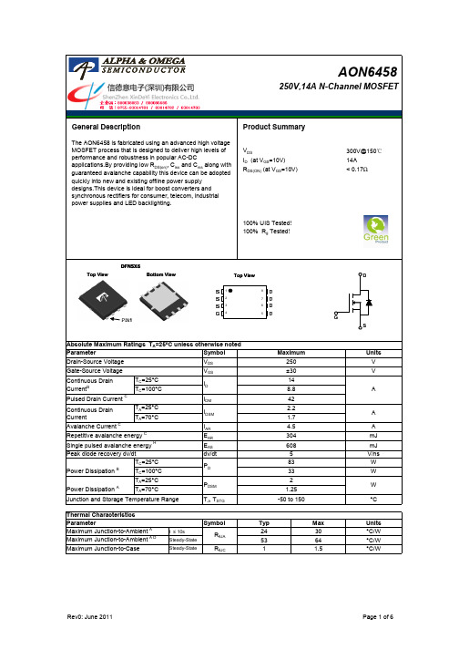
General DescriptionAbsolute Maximum Ratings T =25°C unless otherwise noted Symbol Symbolt ≤ 10s Steady-State Steady-StateR θJCMaximum Junction-to-CaseMaximum Junction-to-Ambient A R θJA Maximum Junction-to-Ambient A D Max 53Units 30°C/W 24ParameterTyp Thermal Characteristics Parameter A Drain-Source Voltage Gate-Source Voltage T =100°C T C =25°C Continuous Drain Current B°C/W°C/W 1641.5DPIN1SymbolMinTypMaxUnits250300BV DSS /∆TJ 0.25V/ o C 110I GSS Gate-Body leakage current ±100n ΑV GS(th)Gate Threshold Voltage3.23.84.5V R DS(ON)0.140.17Ωg FS 16S V SD 0.721V I S Maximum Body-Diode Continuous Current14A I SM42A C iss 81010281240pF C oss 110167225pF C rss 51117pF R g1.9 3.9 5.9ΩQ g 172227nC Q gs 6.3nC Q gd 8nC t D(on)28ns t r 57ns t V DS =5V, I D =250µA V DS =200V, T J =125°C Static Drain-Source On-Resistance V GS =10V, I D =10A V DS =0V, V GS =±30V Maximum Body-Diode Pulsed CurrentInput Capacitance Output CapacitanceDYNAMIC PARAMETERS Turn-On Rise Time Gate Drain Charge Gate Source Charge Reverse Transfer Capacitance V GS =0V, V DS =25V, f=1MHz Gate resistanceElectrical Characteristics (T J =25°C unless otherwise noted)STATIC PARAMETERS ParameterConditionsI DSS Zero Gate Voltage Drain Current V DS =250V, V GS =0V µA V Zero Gate Voltage Drain Current Drain-Source Breakdown Voltage I D =250µA, V GS =0V, T J =25°C I D =250µA, V GS =0V, T J =150°C BV DSS ID=250µA, VGS=0V SWITCHING PARAMETERS Forward Transconductance I S =1A,V GS =0VV DS =40V, I D =10A Total Gate Charge V GS =10V, V DS =200V, I D =10AV GS =10V, V DS =125V, I D =10A,ΩTurn-On DelayTime Diode Forward VoltageV GS =0V, V DS =0V, f=1MHzD(off)65ns t f 40ns t rr 125158190ns Q rr0.811.2µCTHIS PRODUCT HAS BEEN DESIGNED AND QUALIFIED FOR THE CONSUMER MARKET. APPLICATIONS OR USES AS CRITICAL COMPONENTS IN LIFE SUPPORT DEVICES OR SYSTEMS ARE NOT AUTHORIZED. AOS DOES NOT ASSUME ANY LIABILITY ARISING OUT OF SUCH APPLICATIONS OR USES OF ITS PRODUCTS. AOS RESERVES THE RIGHT TO IMPROVE PRODUCT DESIGN,FUNCTIONS AND RELIABILITY WITHOUT NOTICE.Body Diode Reverse Recovery Charge I F =10A,dI/dt=100A/µs,V DS =100VTurn-Off DelayTime Body Diode Reverse Recovery TimeI F =10A,dI/dt=100A/µs,V DS =100VTurn-Off Fall TimeR G =25A. The value of R θJA is measured with the device mounted on 1 in 2FR-4 board with 2oz. Copper, in a still air environment with T A =25°C. The Power Dissipation P DSM is based on R θJA t ≤10s value and the maximum allowed junction temperature of 150°C. The value in any given application depends on the user's specific board design.B. The power dissipation PD is based on T J(MAX)=150°C, using junction-to-case thermal resistance, and is more useful in setting the upper dissipation limit for cases where additional heatsinking is used.C. Repetitive rating, pulse width limited by junction temperature T J(MAX)=150°C. Ratings are based on low frequency and duty cycles to keep initial T J =25°C.D. The R θJA is the sum of the thermal impedance from junction to case R θJC and case to ambient.E. The static characteristics in Figures 1 to 6 are obtained using <300µs pulses, duty cycle 0.5% max.F. These curves are based on the junction-to-case thermal impedance which is measured with the device mounted to a large heatsink, assuming a maximum junction temperature of T J(MAX)=150°C. The SOA curve provides a single pulse rating.G.These tests are performed with the device mounted on 1 in 2 FR-4 board with 2oz. Copper, in a still air environment with T A =25°C.H. L=60mH, I AS =4.5A, V DD =150V, R G =25Ω, Starting T J =25°C.TYPICAL ELECTRICAL AND THERMAL CHARACTERISTICSV 6 I VoltageFigure 4: On-Resistance vs. Junction TemperatureV 401.0E-041.0E-031.0E-021.0E-011.0E+001.0E+011.0E+020.20.40.60.8 1.0I S (A )V SD (Volts)Figure 6: Body-Diode Characteristics25°C125°C051015202530051015202530I D (A )DS (Volts)Figure 1: On-Region Characteristics V GS =5.5V6.0V10V6.5V0.1110100248 10I D (A )V GS (Volts)Figure 2: Transfer Characteristics-55°CV DS =40V25°C125°C0.000.05 0.10 0.15 0.20 0.25 0.30 0510152025R D S (O N )(Ω)D (A)Figure 3: On-Resistance vs. Drain Current and GateV GS =10V00.511.522.53-100-5050100150200N o r m a l i z e d O n -R e s i s t a n c eTemperature (°C)GS =10V I D =10A0.80.911.11.2-100-5050100150200B V D S S (N o r m a l i z e d )T J(o C)Figure 5: Break Down vs. Junction Temperature0.0010.010.11100.0000010.000010.00010.0010.010.1110100Z θJ C N o r m a l i z e d T r a n s i e n t T h e r m a l R e s i s t a n c ePulse Width (s)Figure 11: Normalized Maximum Transient Thermal Impedance (Note F)D=T on /TT J,PK =T C +P DM .Z θJC .R θJCIn descending orderD=0.5, 0.3, 0.1, 0.05, 0.02, 0.01, single pulseSingle PulseT onT P D0.0010.010.11100.00010.0010.010.11101001000Z θJ A N o r m a l i z e d T r a n s i e n t T h e r m a l R e s i s t a n c ePulse Width (s)Figure 15: Normalized Maximum Transient Thermal Impedance (Note G)D=T on /TT J,PK =T A +P DM .Z θJA .R θJA R θJA =64°C/WIn descending orderD=0.5, 0.3, 0.1, 0.05, 0.02, 0.01, single pulseSingle PulseT onTP DVdsC ha rgeVddARGate Charge Test Circuit & W av eformResistiv e Switching Test Circuit & W av eforms VddVdsI dVgsBV I Unclamped Inductive Switching (UIS) Test Circuit & W av eforms I Diode Recovery Vd ARDSS2E = 1/2 LIVdd AR。
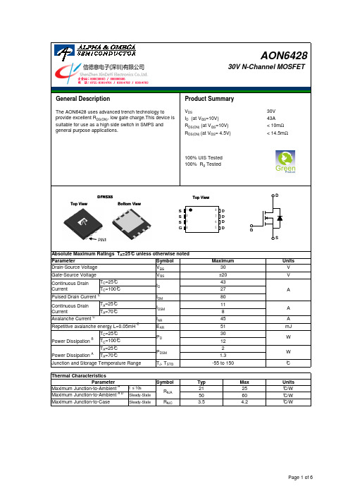
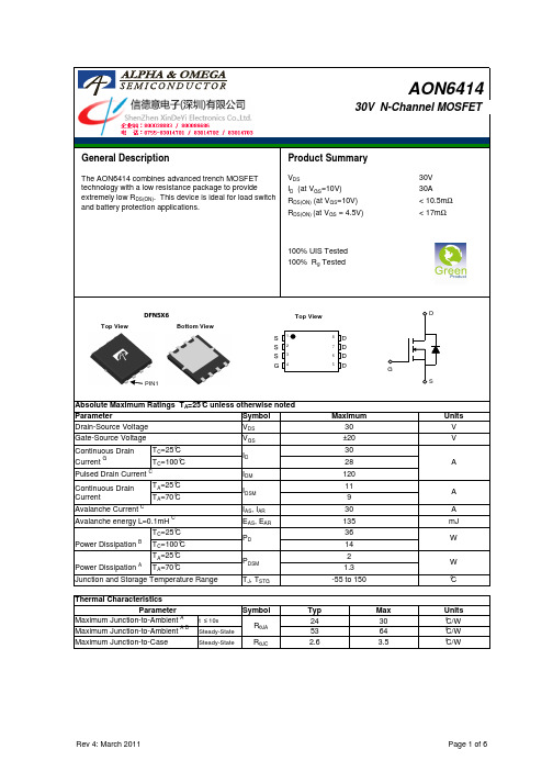
Symbolt ≤ 10s Steady-State Steady-StateR θJCMaximum Junction-to-Case°C/W°C/W Maximum Junction-to-Ambient A D 2.6643.5Power Dissipation B W Power DissipationAW T =70°C T =25°C AT =25°C A T =70°CT =25°C T =100°C Avalanche energy L=0.1mHCmJ Avalanche Current CContinuous Drain CurrentA V MaximumUnits Parameter Absolute Maximum Ratings T A =25°C unless otherwise noted V ±20Gate-Source Voltage Drain-Source Voltage 30Units Maximum Junction-to-Ambient A °C/W R θJA 245330Junction and Storage Temperature Range °CThermal CharacteristicsPulsed Drain Current CContinuous Drain Current GParameterTyp Max T =25°C T =100°C PIN1SymbolMin TypMaxUnits BV DSS 30V V DS =30V, V GS =0V1T J =125°C5I GSS ±100nA V GS(th)Gate Threshold Voltage 1.3 1.92.5V I D(ON)120A 8.710.5T J =125°C13161417m Ωg FS40S V SD 0.721V I S40A C iss 10001300pF C oss 340pF C rss 100pF R g1.32.0ΩQ g (10V)1823nC Q g (4.5V)8.5nC Q gs 3.1nC Q gd 4.8nC t D(on) 5.6ns t r 5.5ns t D(off)18.5ns t f 5ns t rr 2938ns Q rr24nCTHIS PRODUCT HAS BEEN DESIGNED AND QUALIFIED FOR THE CONSUMER MARKET. APPLICATIONS OR USES AS CRITICAL COMPONENTS IN LIFE SUPPORT DEVICES OR SYSTEMS ARE NOT AUTHORIZED. AOS DOES NOT ASSUME ANY LIABILITY ARISING OUT OF SUCH APPLICATIONS OR USES OF ITS PRODUCTS. AOS RESERVES THE RIGHT TO IMPROVE PRODUCT DESIGN,FUNCTIONS AND RELIABILITY WITHOUT NOTICE.Total Gate Charge V GS =10V, V DS =15V, I D =20AGate Drain Charge V GS =0V, V DS =15V, f=1MHz SWITCHING PARAMETERS Total Gate Charge Gate Source Charge Gate resistanceV GS =0V, V DS =0V, f=1MHzTurn-On Rise Time Turn-Off DelayTime V GS =10V, V DS =15V, R L =0.75Ω,R GEN =3ΩTurn-Off Fall TimeTurn-On DelayTime m ΩV GS =4.5V, I D =20AI S =1A,V GS =0VV DS =5V, I D =20A Maximum Body-Diode Continuous CurrentInput Capacitance Output CapacitanceDYNAMIC PARAMETERS R DS(ON)Static Drain-Source On-ResistanceForward Transconductance Diode Forward VoltageV DS =V GS I D =250µA Electrical Characteristics (T J =25°C unless otherwise noted)STATIC PARAMETERS ParameterConditions I DSS Zero Gate Voltage Drain Current µA V DS =0V, V GS = ±20V Gate-Body leakage current Body Diode Reverse Recovery TimeBody Diode Reverse Recovery Charge I F =20A, dI/dt=100A/µsDrain-Source Breakdown Voltage On state drain currentI D =250µA, V GS =0V V GS =10V, V DS =5V V GS =10V, I D =20AReverse Transfer Capacitance I F =20A, dI/dt=100A/µsA: The value of R θJA is measured with the device in a still air environment with T A =25°C.B. The power dissipation P D is based on T J(MAX)=150°C, using junction-to-case thermal resistance, and is more useful in setting the upper dissipation limit for cases where additional heatsink is used.C: Repetitive rating, pulse width limited by junction temperature T J(MAX)=150°C.D. The R θJA is the sum of the thermal impedence from junction to case R θJC and case to ambient.E. The static characteristics in Figures 1 to 6 are obtained using <300 µs pulses, duty cycle 0.5% max.F. These curves are based on the junction-to-case thermal impedence which is measured with the device mounted to a large heatsink,assuming a maximum junction temperature of T J(MAX)=150°C.G. These tests are performed with the device mounted on 1 in 2 FR-4 board with 2oz. Copper, in a still air environment with T A =25°C. The SOA curve provides a single pulse rating.H. Surface mounted on a 1 in 2 FR-4 board with 2oz. Copper.J. Maximum current is limited by bonding wire.TYPICAL ELECTRICAL AND THERMAL CHARACTERISTICSVdsChargeGate Charge Test Circuit & WaveformVdd90%Resistive Switching Test Circuit & WaveformsVddVdsIdVgsBV IUnclamped Inductive Switching (UIS) Test Circuit & WaveformsARDSS2E = 1/2 LI Vdd AR AR。


***********规格书
***********规格书简介如下:
该产品是一款电子元器件,属于连接器、互连器件类别,特别适用于家庭背板连接器,符合DIN 41612系列标准。
其主要特性包括接头类型为母引脚,具有48个针脚的电源接口,间距为0.200"(即5.08mm)。
此外,该产品的触点材料采用铜合金,具有优良的导电性能。
在额定电流6A、额定电压125V交流的条件下,该产品能稳定工作。
以下是***********规格书的相关信息:
型号:***********
类别:连接器,互连器件,家庭背板连接器,DIN 41612系列
包装:散装
连接器类型:接头,母引脚
针脚数:48(电源)
间距:0.200"(5.08mm)
触点材料:铜合金
额定电流:6A
额定电压:125V交流
以上信息可能并不完整,建议访问电子元器件相关网站或咨询相关厂商,以获取更详细、准确的规格书信息。
同时,请注意选择正规渠道购买电子元器件,以确保产品质量和售后服务。
Pomona®All dimensions are in inches. Tolerances (except noted): .xx = ±.02” (,51 mm), .xxx = ± .005” (,127 mm).All specifications are to the latest revisions. Specifications are subject to change without notice.Registered trademarks are the property of their respective companies. Made in USA6/9/99Pomona ACCESS 90601 (800) 444-6785 or (425) 446-6010 SY/EH/LS More drawings available at Page 1 of 1 Model 4684 Adapter – BNC Female To Banana Plug With Ground LeadSales: 800-490-2361 Fax: 888-403-3360 Technical Assistance: 800-241-2060 FEATURES:• Permits BNC male to be used with equipment having standard banana jacks.• Allows the ground jack to be located up to 63,5 (2.50) away from the output/input jack.MATERIALS:Upper Conn: BNC FemaleFinish: Body – Tarnish resistant.Center Contact – Gold plated per requirements of MIL-C-39012.Insulation: Polypropylene molded to connector, plug body and wire.Color: Red.Marking: “POMONA 4684.”Ground Lead: In-line Banana Plug. Spring – Beryllium Copper per QQ-C-533, Alloy 172,Cond. H.T.Material: Body – Brass per QQ-B-626, Alloy 360, ½ Hard.Finish: Nickel plated per QQ-N-290, Class 2, 200/300 microinches.Wire: 18 AWG, stranding 65 x 36 t.c., PVC insulated, 3.66 (.144) O.D.Color: BlackBanana Plug Insulation: Polypropylene molded to plug body and wire.Color: Black.Lower Conn: Banana PlugMaterial: Spring – Beryllium Copper per QQ-C-533, Alloy 172, Cond. H.T.Body – Brass per QQ-B-626, Alloy 360, ½ Hard.Finish: Nickel plated per QQ-N-290, Class 2, 200/300 microinches.RATINGS:Operating Temperature: +55º C. (+131º F.) Max.Voltage: Hand-held Testing: 30VAC/60VEDC Max.Hand Free Testing in Controlled Voltage Environments: 500 VRMS Max.ORDERING INFORMATION: Model 4684/分销商库存信息: POMONA4684。