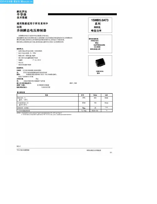
MTAN2135-CG中文资料
- 格式:pdf
- 大小:50.86 KB
- 文档页数:1
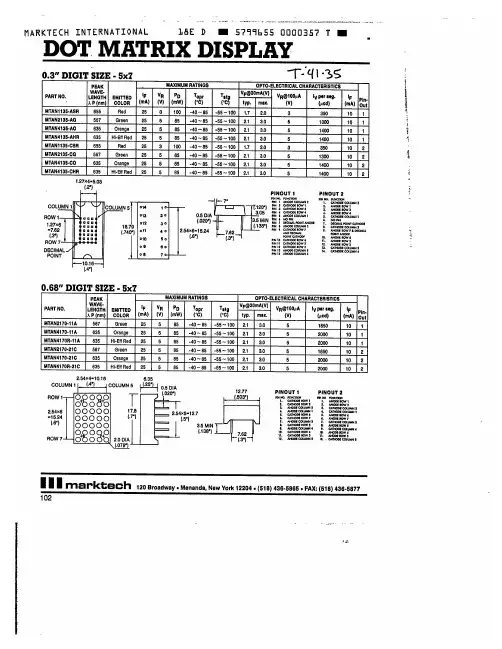

Features•SPI-compatible serial bus interface•Single and double transfer rate (STR/DTR)•Clock frequency–166 MHz (MAX) for all protocols in STR –90 MHz (MAX) for all protocols in DTR•Dual/quad I/O commands for increased through-put up to 90 MB/s•Supported protocols in both STR and DTR –Extended I/O protocol –Dual I/O protocol –Quad I/O protocol •Execute-in-place (XIP)•PROGRAM/ERASE SUSPEND operations•Volatile and nonvolatile configuration settings •Software reset•Additional reset pin for selected part numbers•Dedicated 64-byte OTP area outside main memory –Readable and user-lockable–Permanent lock with PROGRAM OTP command •Erase capability –Bulk erase–Sector erase 64KB uniform granularity –Subsector erase 4KB, 32KB granularity •Security and write protection–Volatile and nonvolatile locking and software write protection for each 64KB sector –Nonvolatile configuration locking –Password protection–Hardware write protection: nonvolatile bits (BP[3:0] and TB) define protected area size –Program/erase protection during power-up –CRC detects accidental changes to raw data •Electronic signature–JEDEC-standard 3-byte signature (BB18h)–Extended device ID: two additional bytes identify device factory options •JESD47H-compliant–Minimum 100,000 ERASE cycles per sector –Data retention: 20 years (TYP)OptionsMarking•Voltage – 1.7–2.0V U •Density –128Mb128•Device stacking –MonolithicA •Device generationB •Die revisionA •Pin configuration–RESET# and HOLD#8•Sector Size –64KBE •Packages – JEDEC-standard, RoHS-compliant–24-ball T-PBGA, 05/6mm x 8mm (5 x 5 array)12–24-ball T-PBGA 05/6mm x 8mm (4 x 6 array)14–Wafer level chip-scale package,15balls , 9 active balls (XFWLBGA 0.5P)54–8-pin SOP2, 208 mils body width (SO8W)SE –16-pin SOP2, 300 mils body width (SO16W)SF –W-PDFN-8 6mm x 5mm (MLP8 6mm x 5mm)W7–W-PDFN-8 8mm x 6mm (MLP8 8mm x 6mm)W9•Standard security 0•Special options –Standard S –AutomotiveA •Operating temperature range –From –40°C to +85°C IT –From –40°C to +105°CAT找Memory 、FPGA 、二三极管、连接器、模块、光耦、电容电阻、单片机、处理器、晶振、传感器、 滤波器,上深圳市美光存储技术有限公司Signal Assignments – Package Code: SE, W7, W9Figure 7: 8-Pin, SOP2 or W-PDFN (Top View)12348765S#DQ1W#/DQ2V SS1MT25QXXXXXXX 3EXX-XXXXS#DQ1W#/DQ2V SSV CC DQ3/HOLD#C DQ0V CC DQ3/RESET#C DQ0Notes:1.RESET# or HOLD# signals can share pin 7 with DQ3, depending on the selected device(see Part Numbering Ordering Information). When using single and dual I/O commands on these parts, DQ3 must be driven HIGH by the host, or an external pull-up resistor must be placed on the PCB, in order to avoid allowing the HOLD# or RESET# input to float.2.On the underside of the W-PDFN package, there is an exposed central pad that is pulledinternally to V SS . It can be left floating or can be connected to V SS . It must not be con-nected to any other voltage or signal line on the PCB.3.MT25QXXXXXXX8EXX-XXXX not available in 8-pin package.Signal Assignments – Package Code: SFFigure 8: 16-Pin, Plastic Small Outline – SO16 (Top View)12345678161514131211109C DQ0V SS W#/DQ2DQ3/HOLD#V CC RESET#DNU DNU DNU DNU DNU DNU DNU C DQ0V SS W#/DQ2DNU DNU DNU DNU C DQ0V SS W#/DQ2DNU DNU DNU DNU S#DQ1DQ3/HOLD#V CC DNUDNU DNUDNU S#DQ1DQ3/RESET#V CC DNU DNUDNU DNU S#DQ18MT25QXXXXXXX 3EXX-XXXXMT25QXXXXXXX 1EXX-XXXX Notes:1.RESET# or HOLD# signals can share pin 1 with DQ3, depending on the selected device(see Part Numbering Ordering Information). When using single and dual I/O commands on these parts, DQ3 must be driven HIGH by the host, or an external pull-up resistor must be placed on the PCB, in order to avoid allowing the HOLD# or RESET# input to float.128Mb, 1.8V Multiple I/O Serial Flash Memory Signal Assignments – Package Code: SE, W7, W9128Mb, 1.8V Multiple I/O Serial Flash Memory Signal Assignments – Package Code: SF128Mb, 1.8V Multiple I/O Serial Flash MemorySignal Descriptions128Mb, 1.8V Multiple I/O Serial Flash Memory Package Dimensions – Package Code: 12Notes: 1.All dimensions are in millimeters.。
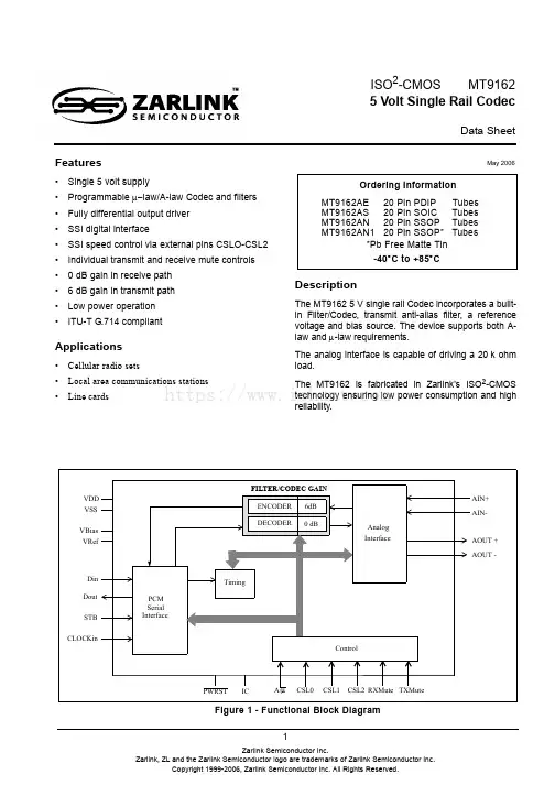
1Features•Single 5 volt supply•Programmable µ−law/A-law Codec and filters •Fully differential output driver •SSI digital interface•SSI speed control via external pins CSLO-CSL2•Individual transmit and receive mute controls •0dB gain in receive path •6dB gain in transmit path •Low power operation •ITU-T G.714 compliantApplications•Cellular radio sets•Local area communications stations •Line cardsDescriptionThe MT9162 5V single rail Codec incorporates a built-in Filter/Codec, transmit anti-alias filter, a reference voltage and bias source. The device supports both A-law and µ-law requirements.The analog interface is capable of driving a 20k ohm load.The MT9162 is fabricated in Zarlink's ISO 2-CMOS technology ensuring low power consumption and high reliability.May 2006Ordering InformationMT9162AE 20 Pin PDIP Tubes MT9162AS 20 Pin SOIC Tubes MT9162AN 20 Pin SSOP Tubes MT9162AN120 Pin SSOP*Tubes*Pb Free Matte Tin-40°C to +85°CISO 2-CMOS MT9162 5 Volt Single Rail CodecData SheetFigure 1 - Functional Block Diagramhttps://MT9162Data SheetFigure 2 - Pin ConnectionsPin Description Pin # Name Description1V Bias Bias Voltage (Output). (V DD /2) volts is available at this pin for biasing external amplifiers. Connect 0.1 µ F capacitor to V SS . Connect 1 µF capacitor to Vref.2V RefReference Voltage for Codec (Output). Nominally [(V DD /2)-1.9] volts. Used internally. Connect 0.1 µ F capacitor to V SS . Connect 1 µF capacitor to VBias3PWRST Power-up Reset. Resets internal state of device via Schmitt Trigger input (active low).4IC Internal Connection. Tie externally to V SS for normal operation.5A/µA/µ Law Selection . CMOS level compatible input pin governs the companding law used by the device. A-law selected when pin tied to V DD or µ-law selected when pin tied to V SS .6RXMute Receive Mute. When 1, the transmit PCM is forced to negative zero code. When 0, normal operation.CMOS level compatible.7TXMute Transmit Mute. When 1, the transmit PCM is forced to negative zero code. When 0, normal operation.CMOS level compatible.8910CSL0CSL1CSL2Clock Speed Select. These pins are used to program the speed of the SSI mode as well as the conversion rate between the externally supplied MCL clock and the 512 kHz clock required by the filter/codec. Refer to Table 2 for details. CMOS level compatible.11D outData Output. A tri-state digital output for 8-bit wide channel data being sent to the Layer 1 device. Data is shifted out via the pin concurrent with the rising edge of BCL during the timeslot defined by STB.12D in Data Input. A digital input for 8-bit wide data from the layer 1 device. Data is sampled on the falling edge of BCL during the timeslot defined by STB. CMOS level compatible.13STBData Strobe. This input determines the 8-bit timeslot used by the device for both transmit and receive data. This active high signal has a repetition rate of 8 kHz. CMOS level compatible.14CLOCKin Clock (Input). The clock provided to this input pin is used by the internal device functions. Connect bitclock to this pin when it is 512 kHz or greater. Connect a 4096 kHz clock to this pin when the bit clock is 128 kHz or 256 kHz. CMOS level compatible.15V DDPositive Power Supply. Nominally 5 volts.AIN-AIN+VBias VRef IC RXMUTE CSL0CSL1CSL2Din DoutVSS AOUT +AOUT -VDD1234567891011121314151620191817PWRSTTXMUTESTB CLOCKin 20 PIN PDIP/SOIC/SSOP A/µhttps://MT9162Data SheetOverviewThe 5V single rail Codec features complete Analog/Digital and Digital/Analog conversion of audio signals (Filter/Codec) and an analog interface to a standard analog transmitter and receiver (Analog Interface). The receiver amplifier is capable of driving a 20k ohm load.Functional DescriptionFilter/CodecThe Filter/Codec block implements conversion of the analog 0-3.3 kHz speech signals to/from the digital domain compatible with 64 kb/s PCM B-Channels. Selection of companding curves and digital code assignment are programmable. These are ITU-T G.711 A-law or µ-Law, with true-sign/Alternate Digit Inversion.The Filter/Codec block also implements a transmit audio path gain in the analog domain. Figure 3 depicts the nominal half-channel for the MT9162.The internal architecture is fully differential to provide the best possible noise rejection as well as to allow a wide dynamic range from a single 5 volt supply design. This fully differential architecture is continued into the analog interface section to provide full chip realization of these capabilities for the external functions.A reference voltage (V Ref ), for the conversion requirements of the Codec section, and a bias voltage (V Bias ), for biasing the internal analog sections, are both generated on-chip. V Bias is also brought to an external pin so that it may be used for biasing external gain setting amplifiers. A 0.1µF capacitor must be connected from V Bias to analog ground at all times. Likewise, although V Ref may only be used internally, a 0.1µF capacitor from the V Ref pin to ground is required at all times. The analog ground reference point for these two capacitors must be physically the same point. To facilitate this the V Ref and V Bias pins are situated on adjacent pins.The transmit filter is designed to meet ITU-T G.714 specifications. An anti-aliasing filter is included. This is a second order lowpass implementation with a corner frequency at 25 kHz.The receive filter is designed to meet ITU-T G.714 specifications. Filter response is peaked to compensate for the sinx/x attenuation caused by the 8 kHz sampling rate.Companding law selection for the Filter/Codec is provided by the A/ µ companding control pin. Table 1 illustrates these choices.16AOUT-Inverting Analog Output. (balanced).17AOUT+Non-Inverting Analog Output. (balanced).18V SS Ground. Nominally 0 volts.19Ain-Inverting Analog Input. No external anti-aliasing is required.20Ain+Non-Inverting Analog Input. Non-inverting input. No external anti-aliasing is required.Pin Description (continued)Pin # Name Descriptionhttps://MT9162Data SheetTable 1 - Law SelectionAnalog InterfacesStandard interfaces are provided by the MT9162. These are:•The analog inputs (transmitter), pins AIN+/AIN-. The maximum peak to peak input is 3.667Vpp µ−law and across AIN+/AIN- 3.8Vpp A-law.•The analog outputs (receiver), pins AOUT+/AOUT-.This internally compensated fully differential output driver is capable of driving a load of 20k ohms.PCM Serial InterfaceA serial link is required to transport data between the MT9162 and an external digital transmission device. The MT9162 utilizes the strobed data interface found on many standard Codec devices. This interface is commonly referred to as Simple Serial Interface (SSI).The required mode of operation is selected via the CSL2-0 control pins. See Table 2 for selections based in CSL2-0 pin settings.Quiet CodeThe PCM serial port can be made to send quiet code to the decoder and receive filter path by setting the RxMute pin high. Likewise, the PCM serial port will send quiet code in the transmit path when theFigure 2 - Table 2: Bit Clock Rate SelectionTxMute pin is high. When either of these pins are low their respective paths function normally. The -Zero entry of Table 1 is used for the quiet code definition.Code ITU-T (G .711)µ -Law A-Law + Full Scale 1000 00001010 1010+ Zero 1111 11111101 0101-Zero (quiet code)0111 11110101 0101- Full Scale0000 00000010 1010CSL 2CSL 1CSL 0External Clock Bit Rate (kHz)CLOCKin (kHz)10012840961012564096000512512001153615360102048204801140964096https://MT9162Data SheetSSI ModeThe SSI BUS consists of input and output serial data streams named Din and Dout respectively, a Clock input signal (CLOCKin), and a framing strobe input (STB). A 4.096 MHz master clock is also required for SSI operation if the bit clock is less than 512kHz. The timing requirements for SSI are shown in Figures 5 & 6.In SSI mode the MT9162 supports only B-Channel operation. Hence, in SSI mode transmit and receive B-Channel data are always in the channel defined by the STB input.The data strobe input STB determines the 8-bit timeslot used by the device for both transmit and receive data. This is an active high signal with an 8 kHz repetition rate.SSI operation is separated into two categories based upon the data rate of the available bit clock. If the bit clock is 512 kHz or greater then it is used directly by the internal MT9162 functions allowing synchronous operation. If the available bit clock is 128 kHz or 256 kHz, then a 4096 kHz master clock is required to derive clocks for the internal MT9162 functions.Applications where Bit Clock (BCL) is below 512 kHz are designated as asynchronous. The MT9162 will re-align its internal clocks to allow operation when the external master and bit clocks are asynchronous. Control pins CSL2, CSL1 and CSL0 are used to program the bit rates.Figure 3 - Audio Gain PartitioningFor synchronous operation, data is sampled from Din, on the falling edge of BCL during the time slot defined by the STB input. Data is made available, on Dout, on the rising edge of BCL during the time slot defined by the STB input. Dout is tri-stated at all times when STB is not true. If STB is valid, then quiet code will be transmitted on Dout during the valid strobe period. There is no frame delay through the PCM serial circuit for synchronous operation.MT9162Data SheetFor asynchronous operation Dout and Din are as defined for synchronous operation except that the allowed output jitter on Dout is larger. This is due to the resynchronization circuitry activity and will not affect operation since the bit cell period at 128 kb/s and 256 kb/s is relatively large. There is a one frame delay through the PCM serial circuit for asynchronous operation. Refer to the specifications of Figures 5 & 6 for both synchronous and asynchronous SSI timing. PWRSTWhile the MT9162 is held in PWRST no device control or functionality is possible.ApplicationsFigure 4 shows the MT9162 in a line card application.Figure 4 - Line Card Application0.1 µF0.1 µFVBias +5V+5VDC to DC ConverterTwisted Pair+5VDout DinLinZ T Lout1234567891011121314151620191817Frame PulseClockA/µMT9162Typical External GainA V= 5-10()100k 100k 100k 100k 100k 100k 100k 1k1k 1k 1k 1k 1k CS2CS1CS0TxMUTERxMUTE MT8972DNICFrom Digital PhoneOut to Subscriber LineInterfaceInput from SubscriberLine Interface1 µFhttps://MT9162Data Sheet Absolute Maximum Ratings†Parameter Symbol Min.Max.Units 1Supply V oltage V DD - V SS- 0.37V 2V oltage on any I/O pin V I/V O V SS - 0.3V DD + 0.3V 3Current on any I/O pin (transducers excluded)I I/I O± 20mA 4Storage Temperature T S- 65+ 150°C 5Power Dissipation (package)P D750mW†Exceeding these values may cause permanent damage. Functional operation under these conditions is not implied.Recommended Operating Conditions - Voltages are with respect to V SS unless otherwise statedCharacteristics Sym.Min.Typ.Max.Units Test Conditions 1Supply V oltage V DD 4.755 5.25V2CMOS Input V oltage (high)V IHC 4.5V DD V3CMOS Input V oltage (low)V ILC V SS0.5V4Operating Temperature T A- 40+ 85°Chttps://Power CharacteristicsCharacteristics Sym.Min.Typ.Max.Units Test Conditions 1Static Supply Current (clock disabled)I DDC1420µA Outputs unloaded, Inputsignals static, not loaded 2Dynamic Supply Current:Total all functions enabled I DDFT7.010mA See Note 1Note 1: Power delivered to the load is in addition to the bias current requirements.MT9162Data Sheet†DC Electrical Characteristics are over recommended temperature range & recommended power supply voltages.‡Typical figures are at 25 °C and are for design aid only: not guaranteed and not subject to production testing.*Note 1 - Magnitude measurement, ignore signs.†AC Electrical Characteristics are over recommended temperature range & recommended power supply voltages.‡Typical figures are at 25 °C and are for design aid only: not guaranteed and not subject to production testing.DC Electrical Characteristics † - Voltages are with respect to ground (V SS ) unless otherwise stated.CharacteristicsSym.Min.Typ.‡Max.Units Test Conditions1Input HIGH V oltage CMOS inputs V IHC 3.5V2Input LOW V oltage CMOS inputs V ILC 1.5V 3VBias V oltage Output V Bias V DD /2V Max. Load = 10k Ω4V Ref Output V oltage V Ref V DD /2-1.9V No load 5Input Leakage Current I IZ 0.110µA V IN =V DD to V SS6Positive Going Threshold V oltage (PWRST only)Negative Going Threshold V oltage (PWRST only)V T+V T- 3.71.3V V 7Output HIGH Current I OH 37mA V OH = 0.9*V DD See Note 18Output LOW Current I OL 510mA V OL = 0.1*V DD See Note 19Output Leakage Current I OZ 0.0110µA V OUT = V DD and V SS 10Output Capacitance C o15pF11Input CapacitanceC i10pF Clockin Tolerance Characteristics †CharacteristicsMin.Typ.‡Max.Units Test Conditions 1CLOCKin Frequency (Asynchronous Mode)4095.640964096.4kHz(i.e., 100 ppm)https://MT9162Data Sheet†AC Electrical Characteristics are over recommended temperature range & recommended power supply voltages.‡Typical figures are at 25 °C and are for design aid only: not guaranteed and not subject to production testing.AC Characteristics † for A/D (Transmit) Path - 0dBm0 = A Lo3.17 - 3.17dB = 1.773V rms for µ-Law and 0dBm0 = A Lo3.14- 3.14dB = 1.843V rms for A-Law, at the Codec. (V Ref =0.6 volts and V Bias =2.5 volts.)CharacteristicsSym.Min.Typ.‡Max.Units Test Conditions 1Analog input equivalent to overload decisionA Li3.17A Li3.147.3347.6Vp-p Vp-pµ-Law A-LawBoth at Codec2Absolute half-channel gain AIN ± to Dout G AX1 5.2 6.0 6.8dB Transmit filter gain=0dB setting. @1020Hz 3Gain tracking vs. input level ITU-T G .714 Method 2G TX-0.3-0.6-1.60.30.61.6dB dB dB 3 to -40 dBm0-40 to -50 dBm0-50 to -55 dBm04Signal to total Distortion vs. input level.ITU-T G .714 Method 2D QX352924dB dB dB0 to -30 dBm0-40 dBm0-45 dBm05Transmit Idle Channel Noise N CX N PX 8.5-7112-69dBrnC0dBm0p µ-Law A-Law6Gain relative to gain at <50Hz 60Hz 200Hz300 - 3000 Hz 3000 - 3400 Hz 4000 Hz >4600 Hz G RX-0.25-0.9-45-23-40-25-300.00.250.25-12.5-25dB dB dB dB dB dB dB 7Absolute DelayD AX 360µs at frequency of minimum delay8Group Delay relative to D AXD DX750380130750µs µs µs µs500-600 Hz 600 - 1000 Hz 1000 - 2600 Hz 2600 - 2800 Hz 9Power Supply Rejection f=1020 Hz f=0.3 to 3 kHz f=3 to 4 kHz f=4 to 50 kHzPSSR PSSR1PSSR2PSSR33737403540dB dB dB dB±100mV peak signal on V DD µ-lawPSSR1-3 not production testedhttps://MT9162Data Sheet†AC Electrical Characteristics are over recommended temperature range & recommended power supply voltages.‡Typical figures are at 25 °C and are for design aid only: not guaranteed and not subject to production testing.†Electrical Characteristics are over recommended temperature range & recommended power supply voltages.‡Typical figures are at 25 °C and are for design aid only: not guaranteed and not subject to production testing.AC Characteristics † for D/A (Receive) Path - 0dBm0 = A Lo3.17 - 3.17dB = 1.773V rms for µ-Law and 0dBm0 = A Lo3.14- 3.14dB = 1.843V rms for A-Law, at the Codec. (V Ref =0.6 volts and V Bias =2.5 volts.)CharacteristicsSym.Min.Typ.‡Max.Units Test Conditions 1Analog output at the Codec full scaleA Lo3.17A Lo3.147.2257.481Vp-p Vp-p µ-Law A-Law 2Absolute half-channel gain.Din to AOUT ±G AR1-0.800.8dB @1020Hz 3Gain tracking vs. input level ITU-T G .714 Method 2G TR-0.3-0.6-1.60.30.61.6dB dB dB 3 to -40 dBm0-40 to -50 dBm0-50 to -55 dBm04Signal to total distortion vs. input level.ITU-T G .714 Method 2G QR352924dB dB dB 0 to -30 dBm0-40 dBm0-45 dBm05Receive Idle Channel Noise N CR N PR 7-8410-80dBrnC0dBm0p µ-Law A-Law6Gain relative to gain at 1020Hz 200Hz300 - 3000 Hz 3000 - 3400 Hz 4000 Hz >4600 Hz G RR-0.25-0.900.250.250.25-12.5-25dB dB dB dB dB7Absolute DelayD AR240µsat frequency of min. delay 8Group Delay relative to D AR D DR750380130750µs µs µs µs 500-600 Hz600 - 1000 Hz 1000 - 2600 Hz 2600 - 2800 Hz 9CrosstalkD/A to A/D A/D to D/ACT RT CT TR-74-80dB dBG .714.16ITU-TElectrical Characteristics † for Analog OutputsCharacteristicsSym.Min.Typ.‡Max .Units Test Conditions1Load impedance at Output E ZL 20kohms across AOUT ±2Allowable output capacitive loadE CL 20pF each pin:AOUT+, AOUT-3Analog output harmonic distortionE D0.5%20k ohms load across AOUT ±VO ≤693mV RMShttps://MT9162Data Sheet†Electrical Characteristics are over recommended temperature range & recommended power supply voltages.‡Typical figures are at 25 °C and are for design aid only: not guaranteed and not subject to production testing.†Timing is over recommended temperature range & recommended power supply voltages.‡Typical figures are at 25°C and are for design aid only: not guaranteed and not subject to production testing.NOTE 1:Not production tested, guaranteed by design.Electrical Characteristics † for Analog InputsCharacteristicsSym.Min.Typ.‡Max.UnitsTest Conditions1Maximum input voltage without overloading Codec across AIN+/AIN-V IOLH2.903.00Vp-pA/µ = 0 A/µ = 12Input ImpedanceZ I50k ΩAIN+/AIN- to V SSAC Electrical Characteristics † - SSI BUS Synchronous Timing (see Figure 5)CharacteristicsSym.Min.Typ.‡Max.Units Test Conditions 1BCL Clock Period t BCL 2441953ns BCL=4096 kHz to 512 kHz 2BCL Pulse Width High t BCLH 122ns BCL=4096 kHz 3BCL Pulse Width Low t BCLL 122ns BCL=4096 kHz 4BCL Rise/Fall Time t R /t F 20ns Note 15Strobe Pulse Widtht ENW8 x t BCLns Note 16Strobe setup time before BCL falling t SSS70t BCL-80ns 7Strobe hold time after BCL falling t SSH 80t BCL -80ns 8Dout High Impedance to Active Low from Strobe rising t DOZL 50ns C L =150 pF, R L =1K 9Dout High Impedance to Active High from Strobe rising t DOZH 50ns C L =150 pF, R L =1K 10Dout Active Low to High Impedancefrom Strobe falling t DOLZ 50ns C L =150 pF, R L =1K 11Dout Active High to High Impedancefrom Strobe falling t DOHZ 50ns C L =150 pF, R L =1K 12Dout Delay (high and low) from BCLrising t DD 50ns C L =150 pF, R L =1K13Din Setup time before BCL falling t DIS 20ns 14Din Hold Time from BCL fallingt DIH50nshttps://MT9162Data SheetFigure 5 - SSI Synchronous Timing Diagram†Timing is over recommended temperature range & recommended power supply voltages.‡Typical figures are at 25°C and are for design aid only: not guaranteed and not subject to production testing.AC Electrical Characteristics † - SSI BUS Asynchronous Timing (note 1) (see Figure 6)CharacteristicsSym.Min.Typ.‡Max.Units Test Conditions 1Bit Cell Period T DATA 78123906ns ns BCL=128 kHz BCL=256 kHz2Frame JitterT j 600ns 3Bit 1 Dout Delay from STB going high t dda1T j +600ns C L =150 pF, R L =1K 4Bit 2 Dout Delay from STB going high t dda2600+T DATA -T j 600+T DATA 600 +T DATA +T j ns C L =150 pF, R L =1K 5Bit n Dout Delay from STB going hight ddan600 +(n-1) x T DATA -T j 600 +(n-1) x T DATA600 +(n-1) x T DATA +T j nsC L =150 pF, R L =1K n=3 to 86Bit 1 Data BoundaryT DATA1T DATA -T j T DATA +T j ns 7Din Bit n Data Setup time from STB risingt SUT DATA \2+500ns-T j +(n-1) x T DATA nsn=1-88Din Data Hold time from STB risingt hoT DATA \2+500ns+T j +(n-1) x T DATAns(BCL)DinDoutSTB70%30%70%30%70%30%70%30%t BCLHt Rt Ft BCLLt DISt DIHt DOZLt DDt BCLt DOZHt SSSt ENWt SSHt DOLZ t DOHZNOTE:Levels refer to% V DD (CMOS I/O)CLOCKin https://MT9162Data SheetFigure 6 - SSI Asynchronous Timing Diagramhttps://MT9162Data SheetPlastic Dual-In-Line Packages (PDIP) - E SuffixDIM8-Pin16-Pin18-Pin20-Pin PlasticPlastic PlasticPlastic MinMaxMinMax MinMax MinMax A 0.210 (5.33)0.210 (5.33)0.210 (5.33)0.210 (5.33)A 20.115 (2.93)0.195 (4.95)0.115 (2.93)0.195 (4.95)0.115 (2.93)0.195 (4.95)0.115 (2.93)0.195 (4.95)B 0.014(0.356)0.022 (0.558)0.014 (0.356)0.022 (0.558)0.014 (0.356)0.022 (0.558)0.014 (0.356)0.022 (0.558)B 10.045 (1.15)0.070 (1.77)0.045 (1.15)0.070 (1.77)0.045 (1.15)0.070 (1.77)0.045 (1.15)0.070 (1.77)C 0.008(0.204)0.015 (0.381)0.008 (0.204)0.015 (0.381)0.008 (0.204)0.015 (0.381)0.008 (0.204)0.015 (0.381)D 0.348 (8.84)0.430 (10.92)0.745 (18.93)0.840 (21.33)0.845 (21.47)0.925 (23.49)0.925 (23.49) 1.060 (26.9)D 10.005 (0.13)0.005 (0.13)0.005 (0.13)0.005 (0.13)E 0.290 (7.37)0.330 (8.38)0.290 (7.37)0.330 (8.38)0.290 (7.37)0.330 (8.38)0.290 (7.37)0.330 (8.38)E 10.240 (6.10)0.280 (7.11)0.240 (6.10)0.280 (7.11)0.240 (6.10)0.280 (7.11)0.240 (6.10)0.280 (7.11)e 0.100 BSC (2.54)0.100 BSC (2.54)0.100 BSC (2.54)0.100 BSC (2.54)e 1e A 0.300 BSC (7.62)0.300 BSC (7.62)0.300 BSC (7.62)0.300 BSC (7.62)L0.115 (2.93)0.160 (4.06)0.115 (2.93)0.160 (4.06)0.115 (2.93)0.160 (4.06)0.115 (2.93)0.160 (4.06)https://MT9162Data SheetS a15°15°15°15°DIM8-Pin16-Pin 18-Pin 20-Pin PlasticPlasticPlasticPlasticMinMaxMinMaxMinMaxMinMaxhttps://MT9162Data SheetDIM16-Pin18-Pin20-Pin24-Pin28-PinMinMax MinMax MinMax MinMax MinMax A 0.093(2.35)0.104(2.65)0.093(2.35)0.104(2.65)0.093(2.35)0.104(2.65)0.093(2.35)0.104(2.65)0.093(2.35)0.104(2.65)A 10.004(0.10)0.012(0.30)0.004(0.10)0.012(0.30)0.004(0.10)0.012(0.30)0.004(0.10)0.012(0.30)0.004(0.10)0.012(0.30)B 0.014(0.351)0.019(0.488)0.014(0.351)0.019(0.488)0.014(0.351)0.019(0.488)0.014(0.351)0.019(0.488)0.014(0.351)0.019(0.488)C 0.009(0.231)0.013(0.318)0.009(0.231)0.013(0.318)0.009(0.231)0.013(0.318)0.009(0.231)0.013(0.318)0.009(0.231)0.013(0.318)D 0.398(10.1)0.413(10.5)0.447(11.35)0.469(11.90)0.496(12.60)0.518(13.00)0.598(15.2)0.614(15.6)0.697(17.7)0.712(18.1)E 0.291(7.40)0.305(7.75)0.291(7.40)0.305(7.75)0.291(7.40)0.305(7.75)0.291(7.40)0.305(7.75)0.291(7.40)0.305(7.75)e 0.050 BSC (1.27 BSC)0.050 BSC (1.27 BSC)0.050 BSC (1.27 BSC)0.050 BSC (1.27 BSC)0.050 BSC (1.27 BSC)F0.044(1.125)0.064(1.625)0.044(1.125)0.064(1.625)0.044(1.125)0.064(1.625)0.044(1.125)0.064(1.625)0.044(1.125)0.064(1.625)Pin 1A 1BeFEALHCGNotes:1) Not to scale2) Dimensions in inches3) (Dimensions in millimeters)4) O1 & O2 are SYMMETRY dimensions5) A & B Maximum dimensions include allowable mold flashDL4 mils (lead coplanarity)https://MT9162Data SheetLead SOIC Package - S SuffixG 0.040(1.016)0.050(1.270)0.040(1.016)0.050(1.270)0.040(1.016)0.050(1.270)0.040(1.016)0.050(1.270)0.040(1.016)0.050(1.270)H 0.394(10.00)0.419(10.65)0.394(10.00)0.419(10.65)0.394(10.00)0.419(10.65)0.394(10.00)0.419(10.65)0.394(10.00)0.419(10.65)L0.016(0.40)0.050(1.27)0.016(0.40)0.050(1.27)0.016(0.40)0.050(1.27)0.016(0.40)0.050(1.27)0.016(0.40)0.050(1.27)DIM16-Pin18-Pin20-Pin24-Pin28-PinMinMax Min Max Min Max Min Max MinMax https://MT9162Data SheetSmall Shrink Outline Package (SSOP) - N SuffixPin 1A 1BeDFEALHCG Dim 20-Pin 24-Pin28-Pin48-Pin MinMax Min Max MinMax Min Max A 0.079(2)-0.079(2)0.079(2)0.095(2.41)0.110(2.79)A 10.004(0.1)0.004(0.1)0.004(0.1)0.008(0.2)0.015(0.4)B 0.0087(0.22)0.013(0.33)0.0087(0.22)0.013(0.33)0.0087(0.22)0.013(0.33)0.008(0.2)0.0135(0.34)C 0.008(0.21)0.008(0.21)0.008(0.21)0.010(0.25)D 0.27(6.9)0.295(7.5)0.31(7.9)0.33(8.5)0.39(9.9)0.41(10.5)0.62(15.75)0.63(16.00)E 0.2(5.0)0.22(5.6)0.2(5.0)0.22(5.6)0.2(5.0)0.22(5.6)0.291(7.39)0.299(7.59)e 0.025 BSC (0.65 BSC)0.025 BSC (0.65 BSC)0.025 BSC (0.65 BSC)0.025 BSC (0.65 BSC)F 0.049 REF (1.25 REF)0.049 REF (1.25 REF)0.049 REF (1.25 REF)0.056 REF (1.42 REF)G 0.065(1.65)0.073(1.85)0.065(1.65)0.073(1.85)0.065(1.65)0.073(1.85)0.089(2.25)0.099(2.52)H 0.29(7.4)0.32(8.2)0.29(7.4)0.32(8.2)0.29(7.4)0.32(8.2)0.395(10.03)0.42(10.67)L0.022(0.55)0.037(0.95)0.022(0.55)0.037(0.95)0.022(0.55)0.037(0.95)0.02(0.51)0.04(1.02)Notes:1) Not to scale2) Dimensions in inches3) (Dimensions in millimeters)4) Ref. JEDEC Standard M0-1505) A & B Maximum dimensions include allowable mold flashhttps://。