MAX5048AAUT-T中文资料
- 格式:pdf
- 大小:658.51 KB
- 文档页数:11
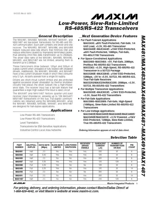
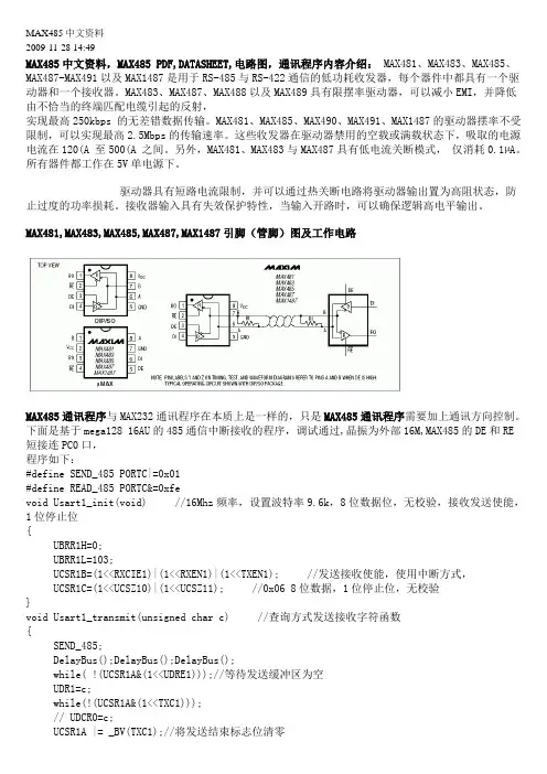
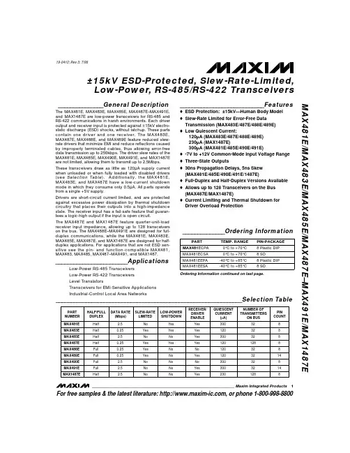
General DescriptionThe MAX5048A/MAX5048B are high-speed MOSFET drivers capable of sinking/sourcing 7.6A/1.3A peak cur-rents. These devices take logic input signals and drive a large external MOSFET. The MAX5048A/MAX5048B have inverting and noninverting inputs that give the user greater flexibility in controlling the MOSFET. They feature two separate outputs working in complementary mode, offering flexibility in controlling both turn-on and turn-off switching speeds.The MAX5048A/MAX5048B have internal logic circuitry,which prevents shoot-through during output state changes. The logic inputs are protected against volt-age spikes up to +14V, regardless of V+ voltage.Propagation delay time is minimized and matched between the inverting and noninverting inputs. The MAX5048A/MAX5048B have very fast switching times combined with very short propagation delays (12ns typ), making them ideal for high-frequency circuits.The MAX5048A/MAX5048B operate from a +4V to +12.6V single power supply and typically consume 0.95mA of supply current. The MAX5048A has CMOS input logic levels, while the MAX5048B has standard TTL input logic levels. These devices are available in space-saving 6-pin SOT23 and TDFN packages.ApplicationsPower MOSFET Switching Switch-Mode Power Supplies DC-DC Converters Motor ControlPower-Supply ModulesFeatures♦Independent Source-and-Sink Outputs for Controllable Rise and Fall Times ♦+4V to +12.6V Single Power Supply ♦7.6A/1.3A Peak Sink/Source Drive Current ♦0.23ΩOpen-Drain n-Channel Sink Output ♦2ΩOpen-Drain p-Channel Source Output ♦12ns (typ) Propagation Delay♦Matching Delay Time Between Inverting and Noninverting Inputs ♦V CC /2 CMOS (MAX5048A)/TTL (MAX5048B) Logic Inputs ♦1.6V Input Hysteresis♦Up to +14V Logic Inputs (Regardless of V+Voltage)♦Low Input Capacitance: 2.5pF (typ)♦-40°C to +125°C Operating Temperature Range ♦6-Pin SOT23 and TDFN PackagesMAX50487.6A, 12ns, SOT23/TDFN, MOSFET Driver________________________________________________________________Maxim Integrated Products1Pin ConfigurationsOrdering InformationTypical Operating Circuit19-2419; Rev 4; 7/05For pricing, delivery, and ordering information,please contact Maxim/Dallas Direct!at 1-888-629-4642, or visit Maxim’s website at .M A X 50487.6A, 12ns, SOT23/TDFN, MOSFET DriverABSOLUTE MAXIMUM RATINGSELECTRICAL CHARACTERISTICSStresses beyond those listed under “Absolute Maximum Ratings” may cause permanent damage to the device. These are stress ratings only, and functional operation of the device at these or any other conditions beyond those indicated in the operational sections of the specifications is not implied. Exposure to absolute maximum rating conditions for extended periods may affect device reliability.Voltages Referenced to GNDV+...........................................................................-0.3V to +13V IN+, IN-...................................................................-0.3V to +14V N_OUT, P_OUT ............................................-0.3V to (V+ + 0.3V)N_OUT Continuous Output Current (Note 1)....................390mA P_OUT Continuous Output Current (Note 1).....................100mA Continuous Power Dissipation* (T A = +70°C)6-Pin SOT23 (derate 9.1mW/°C above +70°C)............727mWJunction to Case Thermal Resistance, θJC (SOT23)....75°C/W 6-Pin TDFN (derate 18.2mW/°C above +70°C).........1454mW Junction to Case Thermal Resistance, θJC (TDFN)....8.5°C/W Operating Temperature Range .........................-40°C to +125°C Storage Temperature Range.............................-65°C to +150°C Junction Temperature......................................................+150°C Lead Temperature (soldering, 10s).................................+300°CNote 1: Continuous output current is limited by the power dissipation of the package.*As per JEDEC51 standard.MAX50487.6A, 12ns, SOT23/TDFN, MOSFET Driver_______________________________________________________________________________________3ELECTRICAL CHARACTERISTICS (continued)Note 2:All DC specifications are 100% tested at T A = +25°C. Specifications over -40°C to +125°C are guaranteed by design.Note 3:Guaranteed by design, not production tested.M A X 50487.6A, 12ns, SOT23/TDFN, MOSFET Driver 4_______________________________________________________________________________________Typical Operating Characteristics(C L = 1000pF, T A = +25°C, unless otherwise noted.)RISE TIME vs. SUPPLY VOLTAGESUPPLY VOLTAGE (V)R I S E T I M E (n s )10868111417205412FALL TIME vs. SUPPLY VOLTAGESUPPLY VOLTAGE (V)F A L L T I M E (n s )10862.53.54.55.06.02.04123.05.54.0SUPPLY VOLTAGE (V)P R O P A G A T I O N D E L A Y (n s )1086121416182010412PROPAGATION DELAY TIME, LOW-TO-HIGHvs. SUPPLY VOLTAGESUPPLY VOLTAGE (V)P R O P A G A T I O N D E L A Y (n s )1086121416182010412PROPAGATION DELAY TIME, HIGH-TO-LOWvs. SUPPLY VOLTAGESUPPLY CURRENT vs. SUPPLY VOLTAGESUPPLY VOLTAGE (V)S U P P L Y C U R R E N T (m A )1086246810120412SUPPLY CURRENT vs. LOAD CAPACITANCELOAD CAPACITANCE (pF)S U P P L Y C U R R E NT (m A )160012004008000.51.01.52.02.53.03.54.002000SUPPLY CURRENT vs. TEMPERATURETEMPERATURE (°C)S U P P L Y C U R R E N T (m A )1007550250-251.31.41.51.61.71.81.2-50125MAX5048AINPUT THRESHOLD VOLTAGEvs. SUPPLY VOLTAGESUPPLY VOLTAGE (V)I N P U T T H R E S H O L D V O L T A G E (V )1086123456780412MAX5048ASUPPLY CURRENT vs. INPUT VOLTAGEINPUT VOLTAGE (V)S U P P L Y C U R R E N T (m A )1086420.91.01.11.21.31.41.51.61.71.80.8012MAX50487.6A, 12ns, SOT23/TDFN, MOSFET Driver_______________________________________________________________________________________5INPUT VOLTAGE vs. OUTPUT VOLTAGE(V+ = +4V, C L = 5000pF)MAX5048 toc10IN+2V/div OUTPUT 2V/div 20ns/div INPUT VOLTAGE vs. OUTPUT VOLTAGE(V+ = +4V, C L = 10,000pF)MAX5048 toc11IN+2V/divOUTPUT 2V/div20ns/div INPUT VOLTAGE vs. OUTPUT VOLTAGE(V+ = +4V, C L = 5000pF)MAX5048 toc12IN+2V/divOUTPUT 2V/div20ns/divINPUT VOLTAGE vs. OUTPUT VOLTAGE(V+ = +4V, C L = 10,000pF)MAX5048 toc13IN+2V/divOUTPUT 2V/div 20ns/div INPUT VOLTAGE vs. OUTPUT VOLTAGE(V+ = +12V, C L = 5000pF)MAX5048 toc14IN+5V/divOUTPUT 5V/div 20ns/div INPUT VOLTAGE vs. OUTPUT VOLTAGE(V+ = +12V, C L = 10,000pF)MAX5048 toc15IN+5V/divOUTPUT 5V/div20ns/divINPUT VOLTAGE vs. OUTPUT VOLTAGE(V+ = +12V, C L = 5000pF)MAX5048 toc16IN+5V/div OUTPUT 5V/div 20ns/div INPUT VOLTAGE vs. OUTPUT VOLTAGE(V+ = +12V, C L = 10,000pF)MAX5048 toc17IN+5V/divOUTPUT 5V/div20ns/divTypical Operating Characteristics (continued)(C L = 1000pF, T A = +25°C, unless otherwise noted.)M A X 50487.6A, 12ns, SOT23/TDFN, MOSFET Driver 6_______________________________________________________________________________________Detailed DescriptionLogic InputsThe MAX5048A/MAX5048Bs’ logic inputs are protected against voltage spikes up to +14V, regardless of the V+voltage.The low 2.5pF input capacitance of the inputs reduces loading and increases switching speed. These devices have two inputs that give the user greater flexi-bility in controlling the MOSFET. Table 1 shows all pos-sible input combinations.The difference between the MAX5048A and the MAX5048B is the input threshold voltage. The MAX5048A has V CC /2 CMOS logic-level thresholds,while the MAX5048B has TTL logic-level thresholds (see the Electrical Characteristics ). For V+ above 5.5V, V IH (typ) = 0.5x(V+) + 0.8V and V IL (typ) = 0.5x(V+) - 0.8V.As V+ is reduced from 5.5V to 4V, V IH and V IL gradually approach V IH (typ) = 0.5x(V+) + 0.65V and V IL (typ) =0.5x(V+) - 0.65V. Connect IN+ to V+ or IN- to GND when not used. Alternatively, the unused input can be used as an ON/OFF pin (see Table 1).Undervoltage Lockout (UVLO)When V+ is below the UVLO threshold, the N-channel is ON and the P-channel is OFF, independent of the state of the inputs. The UVLO is typically 3.6V with 400mV typical hysteresis to avoid chattering.Driver OutputsThe MAX5048A/MAX5048B provide two separate out-puts. One is an open-drain P-channel, the other an open-drain N-channel. They have distinct current sourc-ing/sinking capabilities to independently control the rise and fall times of the MOSFET gate. Add a resistor in series with P_OUT/N_OUT to slow the correspondingrise/fall time of the MOSFET gate.Applications InformationSupply Bypassing, Device Grounding,and PlacementAmple supply bypassing and device grounding are extremely important because when large external capacitive loads are driven, the peak current at the V+pin can approach 1.3A, while at the GND pin the peak current can approach 7.6A. V CC drops and ground shifts are forms of negative feedback for inverters and, if excessive, can cause multiple switching when the IN-input is used and the input slew rate is low. The device driving the input should be referenced to the MAX5048A/MAX5048B GND pin especially when the IN-input is used. Ground shifts due to insufficient device grounding may disturb other circuits sharing the same AC ground return path. Any series inductance in the V+,P_OUT, N_OUT and/or GND paths can cause oscilla-tions due to the very high di/dt that results when the MAX5048A/MAX5048B are switched with any capacitive load. A 0.1µF or larger value ceramic capacitor is rec-ommended bypassing V+ to GND and placed as close to the pins as possible. When driving very large loads (e.g., 10nF) at minimum rise time, 10µF or more of paral-lel storage capacitance is recommended. A ground plane is highly recommended to minimize ground return resistance and series inductance. Care should be taken to place the MAX5048A/MAX5048B as close as possi-ble to the external MOSFET being driven to further mini-mize board inductance and AC path resistance.Power DissipationPower dissipation of the MAX5048A/MAX5048B con-sists of three components, caused by the quiescent current, capacitive charge and discharge of internal nodes, and the output current (either capacitive or resistive load). The sum of these components must be kept below the maximum power-dissipation limit.L = Logic low H = Logic highMAX50487.6A, 12ns, SOT23/TDFN, MOSFET Driver_______________________________________________________________________________________7The quiescent current is 0.95mA typical. The current required to charge and discharge the internal nodes is frequency dependent (see the Typical Operating Characteristics ). The MAX5048A/MAX5048B power dis-sipation when driving a ground referenced resistive load is:P = D x R ON(MAX)x I LOAD 2where D is the fraction of the period the MAX5048A/MAX5048Bs’ output pulls high, R ON (MAX)is the maxi-mum on-resistance of the device with the output high (P-channel), and I LOAD is the output load current of the MAX5048A/MAX5048B.For capacitive loads, the power dissipation is:P = C LOAD x (V+)2x FREQwhere C LOAD is the capacitive load, V+ is the supply voltage, and FREQ is the switching frequency.Layout InformationThe MOSFET drivers MAX5048A/MAX5048B source-and-sink large currents to create very fast rise and fall edges at the gate of the switching MOSFET. The high di/dt can cause unacceptable ringing if the trace lengths and impedances are not well controlled. Thefollowing PC board layout guidelines are recommended when designing with the MAX5048A/MAX5048B:•Place one or more 0.1µF decoupling ceramic capaci-tor(s) from V+ to GND as close to the device as possi-ble. At least one storage capacitor of 10µF (min)should be located on the PC board with a low resis-tance path to the V+ pin of the MAX5048A/MAX5048B.•There are two AC current loops formed between the device and the gate of the MOSFET being driven.The MOSFET looks like a large capacitance from gate to source when the gate is being pulled low.The active current loop is from N_OUT of the MAX5048A/MAX5048B to the MOSFET gate to the MOSFET source and to GND of the MAX5048A/MAX5048B. When the gate of the MOSFET is being pulled high, the active current loop is from P_OUT of the MAX5048A/MAX5048B to the MOSFET gate to the MOSFET source to the GND terminal of the decoupling capacitor to the V+ terminal of the decoupling capacitor and to the V+ terminal of the MAX5048A/MAX5048B. While the charging current loop is important, the discharging current loop is crit-ical. It is important to minimize the physical distance and the impedance in these AC current paths.M A X 50487.6A, 12ns, SOT23/TDFN, MOSFET Driver 8_______________________________________________________________________________________•In a multilayer PC board, the component surface layer surrounding the MAX5048A/MAX5048B should consist of a GND plane containing the discharging and charging current loops.Chip InformationTRANSISTOR COUNT: 676PROCESS:BiCMOSMAX50487.6A, 12ns, SOT23/TDFN, MOSFET Driver_______________________________________________________________________________________9Pin Configurations (continued)6L S O T .E PSPackage Information(The package drawing(s) in this data sheet may not reflect the most current specifications. For the latest package outline information go to /packages .)M A X 50487.6A, 12ns, SOT23/TDFN, MOSFET Driver 10______________________________________________________________________________________Package Information (continued)(The package drawing(s) in this data sheet may not reflect the most current specifications. For the latest package outline information go to /packages .)MAX50487.6A, 12ns, SOT23/TDFN, MOSFET DriverMaxim cannot assume responsibility for use of any circuitry other than circuitry entirely embodied in a Maxim product. No circuit patent licenses are implied. Maxim reserves the right to change the circuitry and specifications without notice at any time.Maxim Integrated Products, 120 San Gabriel Drive, Sunnyvale, CA 94086 408-737-7600 ____________________11©2005 Maxim Integrated Products Printed USAis a registered trademark of Maxim Integrated Products, Inc.Package Information (continued)(The package drawing(s) in this data sheet may not reflect the most current specifications. For the latest package outline information go to /packages .)元器件交易网。