选择正确的电平转换方案英文
- 格式:pdf
- 大小:287.63 KB
- 文档页数:8

frm[版主]注册:2004-11-12 10:06:06可用积分:229全部积分:229等级:☆新年到,给各位拜年了!!!祝大家新年里,事业精进,财源滚滚!选择正确的电平转换方案原著:TI Corp --Application Report SCEA035A翻译:frm1. 简介在今天的电子电路系统中电压电平的转换基本成为了必须。
例如:一个ASIC的供电为VccA,而I/O器件的供电为VccB。
为了使它们之间正常通信,就需要一个如图1的电平转换(level-translation)方案。
输入电平限值和器件的输出电平主要根据器件采用的工艺技术和供电。
图2显示了不同的供电和元件技术的限值范围。
为了成功的实现两个器件的接口,一定要保证以下的条件:■驱动器件的Voh必须大于接收器件的Vih■驱动器件的Vol必须小于接收器件的Vil■驱动器件的输出电压范围不能超过接收器件的可容忍的I/O电压范围2. 双电源电平转换器件(Dual-Supply Level Translators)2.1 特性双电源的器件是为了满足两类总线或不同供电器件之间的异步通讯的。
这类器件采用双电源:VccA为A端(A side)供电,VccB为B端供电。
对于数据从A到B或B到A都能传输的双向的电平转换器件,方向取决于输入pin DIR的逻辑电平。
如果器件有OE控制,在OE有无效时A端和B端的总线隔离。
TI的双电源器件有各种位宽的应用并几乎覆盖了当前出现的全部的供电应用。
这些器件灵活,易用并能实现双向转换,对于许多电平转换的应用都是理想的选择(译者注:强!)。
它们的电流驱动能力可以使其适合长线及重载的应用。
SN74AVCB324245是一种32位双电源电平转换器件(由四组8位端口组成)。
图3显示了SN74AVCB324245的1.8V转3.3V的一个端口,同时另一个端口实现3.3V到1.8V的转换。
双电源器件的优点:●可以在不同电压结点间灵活的转换●具有电流驱动的能力●具有不同的位宽2.2 产品列表表1汇总了TI的双电源产品。
nmos的电平转换电路英文回答:A level shifting circuit using an NMOS transistor is commonly used to convert voltage levels in digital circuits. It allows signals with different voltage levels to communicate with each other.The basic idea behind an NMOS level shifting circuit is to use the NMOS transistor as a switch to connect or disconnect the input and output voltage levels. When the input voltage is high enough to turn on the NMOS transistor, the output voltage will be pulled down to a low level. On the other hand, when the input voltage is low, the NMOS transistor will be turned off, allowing the output voltageto be pulled up to a high level.Let's take an example to illustrate how an NMOS level shifting circuit works. Suppose we have a digital circuit operating at 3.3V and we want to interface it with anothercircuit operating at 5V. We can use an NMOS level shifting circuit to achieve this.In this example, the 3.3V digital circuit is connected to the gate of the NMOS transistor, and the 5V circuit is connected to the drain of the NMOS transistor. When the input signal from the 3.3V circuit is high, it turns on the NMOS transistor, allowing the 5V circuit to be pulled down to a low level. When the input signal is low, the NMOS transistor is turned off, allowing the 5V circuit to be pulled up to a high level.This level shifting circuit can be used in various applications, such as interfacing different voltage level devices, level shifting in I2C or SPI communication, and voltage level translation in microcontrollers.中文回答:NMOS电平转换电路常用于数字电路中,用于转换不同电平的信号,使其能够相互通信。
应用mosfet lowside driver 的电平变换设计
设计MOSFET低侧驱动电平变换可以按照以下步骤进行:
1. 选择合适的MOSFET型号:根据需要驱动的负载电流和电压,选择适当的MOSFET型号。
确保MOSFET的额定电流和电压能满足设计需求。
2. 确定输入电平:根据控制电路的输出电平确定输入电平(例如5V或
3.3V),这取决于你的控制电路。
3. 设计电平转换电路:为了将输入电平(如5V或3.3V)转换为驱动MOSFET 所需的高电平(一般为12V或15V),你可以使用电平转换电路。
3.1 使用电平转换电路,例如使用逻辑电平转换器或门电路,选择合适的部件和电路拓扑。
3.2 确保电平转换电路能提供足够的电流和速度以快速充放电MOSFET的输入电容。
4. 添加保护电路:根据需要,添加保护电路来保护MOSFET和其他电路元件,例如过电流保护、过温保护等。
5. 选择适当的驱动电路:根据MOSFET的特性和需求,选择合适的驱动电路。
有许多驱动电路可供选择,包括单极性和双极性驱动电路。
6. 进行电路仿真和测试:在实际应用之前,进行电路仿真和测试以确保电路的性能和可靠性。
总结:在设计MOSFET低侧驱动电平变换时,需要针对你的具体需求选择适当的MOSFET、设计电平转换电路、添加保护电路并选择适当的驱动电路。
最后进行电路仿真和测试以验证设计的正确性和可靠性。

电平转换精要-输出信号应有对应电平的输入信号Gene Warzecha, 应用工程经理Maxim公司在电子设计中,电平转换器能使I/O电压不同的器件建立通信。
多年前,I/O的电压通常是匹配的,因为大多数处理器和逻辑器件的工作电压都是5V。
当3.3V电压的器件出现后,它们也可以兼容5V电压。
但现在,伴随着高级工艺的发展,电子设计要能兼容许多更低的I/O电压。
芯片设计者能运用特殊的设计技术使I/O的电压“升高”,但是这些技术会降低生产量,降低品质,增加功耗。
此外,处理器或者其他器件需要由不同的电源供电,每个电源都要兼顾其应用和特殊的I/O电压。
因此,受器件设计差别和多个供电电源的影响,需要相互通信的两个器件可能不能直接通信,因为每个器件有不同的工作电压。
而逻辑电平转换器可以帮助解决这个问题。
理想的逻辑电平转换器(LLT)能在1Hz至1GHz之间正常工作,驱动漏级开路信号像驱动COMS推挽信号一样容易,也能很轻松的驱动长电缆。
但是逻辑电平转换器不是理想器件,一定存在功能上的妥协,因此电平转换器供应商会提供各种样式的转换器以满足不同种类的应用。
逻辑电平转换器基础一个主动双向电平转换器有两种基本组成结构,其中一种如图1所示。
通过管(Pass FET,下文同)的每一边都有一个上拉电阻,门级连接到V bias(通常是V cc1和V cc2中较低的那个电压)。
如果任何一个I/O电压(V i或者V o)连接到地电平,这会使正电压V gs打开FET,同时驱动另一侧I/O电压降到地电平。
如果没有I/O电压为低(两个都悬空),由于上拉电阻的作用,I/O的电压为各自的供电电压(V i或者V o)。
关于这个电路的一些重要结论:●输出信号的下降时间(fall time)主要由驱动器的强度,通过管的导通电阻和信号线的寄生电容决定。
●输出信号的上升时间(rise time)主要由输出端的上拉电阻和信号线的寄生电容决定-假设通过管是即刻关闭的(事实并非如此,为方便此处讨论我们做此假设)●输出端低电平电压总比输入端的低电平电压高,这是欧姆定律决定的。
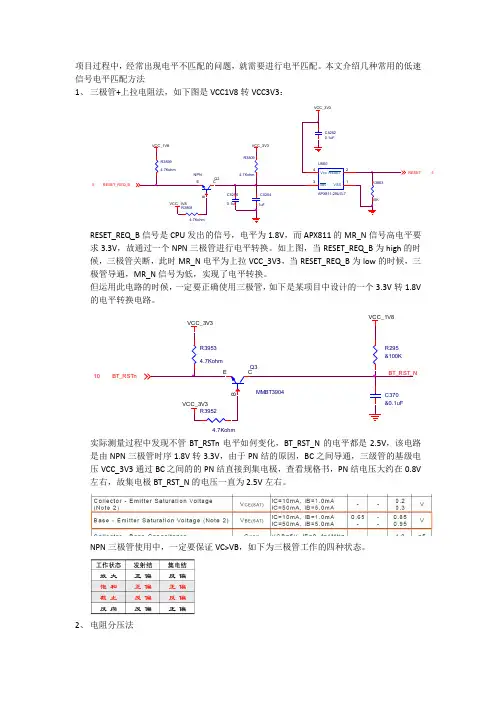
项目过程中,经常出现电平不匹配的问题,就需要进行电平匹配。
本文介绍几种常用的低速信号电平匹配方法1、 三极管+上拉电阻法,如下图是VCC1V8转VCC3V3:RESET_REQ_B 信号是CPU 发出的信号,电平为1.8V ,而APX811的MR_N 信号高电平要求3.3V ,故通过一个NPN 三极管进行电平转换。
如上图,当RESET_REQ_B 为high 的时候,三极管关断,此时MR_N 电平为上拉VCC_3V3,当RESET_REQ_B 为low 的时候,三极管导通,MR_N 信号为低,实现了电平转换。
但运用此电路的时候,一定要正确使用三极管,如下是某项目中设计的一个3.3V 转1.8V 的电平转换电路。
实际测量过程中发现不管BT_RSTn 电平如何变化,BT_RST_N 的电平都是2.5V ,该电路是由NPN 三极管时序1.8V 转3.3V ,由于PN 结的原因,BC 之间导通,三级管的基级电压VCC_3V3通过BC 之间的的PN 结直接到集电极,查看规格书,PN 结电压大约在0.8V 左右,故集电极BT_RST_N 的电压一直为2.5V 左右。
NPN 三极管使用中,一定要保证VC>VB ,如下为三极管工作的四种状态。
2、 电阻分压法RESET_REQ_B5RESET54.7KohmBT_RSTn10电阻分压法只能用于高电平转低电平的电路中,如上中3.3V 转1.8V(VDDS)电路,可以通过电阻分压法进行电平转换。
如下是修改后的电路:3、 使用串阻方法该方法也只适用于高电平转低电平电路,如下:高逻辑电平驱动低逻辑电平时,可串联50Ω~330Ω电阻实现电平的转换,串联电阻的阻值需要根据I/O 口动态电流计算。
4、 使用OD/OC 门芯片+上拉电阻如下图,采用了一个输出为OD 门的buffer 芯片,实现1.8V 转1.35V 的电平转换5、 电平转换芯片专用电平转换芯片主要用于信号速率较高,对信号要求延时等由要求的电路中,如下是MDC/MDIO (SMI )使用的电平转换芯片。
CMOS电平转换电路详解COMS集成电路是互补对称金属氧化物半导体(Compiementary symmetry metal oxide semicoductor)集成电路的英文缩写,电路的许多基本逻辑单元都是用增强型PMOS晶体管和增强型NMOS管按照互补对称形式连接的,静态功耗很小。
COMS电路的供电电压VDD范围比较广在+5~+15V均能正常工作,电压波动允许10,当输出电压高于VDD-0.5V时为逻辑1,输出电压低于VSS+0.5V(VSS为数字地)为逻辑0。
CMOS电路输出高电平约为0.9Vcc,而输出低电平约为0.1Vcc.当输入电压高于VDD-1.5V时为逻辑1,输入电压低于VSS+1.5V(VSS为数字地)为逻辑0。
TTL电平信号被利用的最多是因为通常数据表示采用二进制规定,+5V等价于逻辑1,0V 等价于逻辑0,这被称做TTL(晶体管-晶体管逻辑电平)信号系统,这是计算机处理器控制的设备内部各部分之间通信的标准技术。
标准TTL输入高电平最小2V,输出高电平最小2.4V,典型值3.4V,输入低电平最大0.8V,输出低电平最大0.4V,典型值0.2V(输入H》2V,输入L《0.8V;输出H 》2.4V(3.4V),输出L《0.4V(0.2V)。
CMOS电平是数字信号还是模拟信号?CMOS电平是数字信号,COMS电路的供电电压VDD范围比较广在+5--+15V均能正常工作,电压波动允许10,当输出电压高于VDD-0.5V 时为逻辑1,输出电压低于VSS+0.5V(VSS为数字地)为逻辑0,一般数字信号才是0和1 。
cmos电平转换电路1、TTL电路和CMOS电路的逻辑电平VOH:逻辑电平1 的输出电压VOL:逻辑电平0 的输出电压VIH :逻辑电平1 的输入电压VIH :逻辑电平0 的输入电压TTL电路临界值:。
常用的电平转换方法及注意事项1:常用的电平转换方案(1) 晶体管+上拉电阻法就是一个双极型三极管或 MOSFET,C/D极接一个上拉电阻到正电源,输入电平很灵活,输出电平大致就是正电源电平。
(2) OC/OD 器件+上拉电阻法跟 1) 类似。
适用于器件输出刚好为 OC/OD 的场合。
(3) 74xHCT系列芯片升压(3.3V→5V)凡是输入与 5V TTL 电平兼容的 5V CMOS 器件都可以用作 3.3V→5V 电平转换。
——这是由于 3.3V CMOS 的电平刚好和5V TTL电平兼容(巧合),而 CMOS 的输出电平总是接近电源电平的。
廉价的选择如 74xHCT(HCT/AHCT/VHCT/AHCT1G/VHCT1G/...) 系列 (那个字母 T 就表示 TTL 兼容)。
(4) 超限输入降压法(5V→3.3V, 3.3V→1.8V, ...)凡是允许输入电平超过电源的逻辑器件,都可以用作降低电平。
这里的"超限"是指超过电源,许多较古老的器件都不允许输入电压超过电源,但越来越多的新器件取消了这个限制 (改变了输入级保护电路)。
例如,74AHC/VHC 系列芯片,其 datasheets 明确注明"输入电压范围为0~5.5V",如果采用 3.3V 供电,就可以实现5V→3.3V 电平转换。
(5) 专用电平转换芯片最著名的就是 164245,不仅可以用作升压/降压,而且允许两边电源不同步。
这是最通用的电平转换方案,但是也是很昂贵的 (俺前不久买还是¥45/片,虽是零售,也贵的吓人),因此若非必要,最好用前两个方案。
(6) 电阻分压法最简单的降低电平的方法。
5V电平,经1.6k+3.3k电阻分压,就是3.3V。
(7) 限流电阻法如果嫌上面的两个电阻太多,有时还可以只串联一个限流电阻。
某些芯片虽然原则上不允许输入电平超过电源,但只要串联一个限流电阻,保证输入保护电流不超过极限(如 74HC 系列为 20mA),仍然是安全的。
电平转换方案1. 引言在电子设备和电路设计中,电平转换是一个常见的问题。
不同设备或电路之间可能采用不同的电平标准,如5V、3.3V、2.5V等,为了确保正确的信号传输和兼容性,需要进行电平转换。
本文将介绍电平转换的背景知识、常见的电平转换方案以及各种方案的优缺点。
2. 背景知识2.1 电平标准不同设备或电路常采用不同的电平标准,主要包括:•TTL(Transistor-Transistor Logic)电平:常见的电压标准为0V~5V,适用于许多数字电路。
•CMOS(Complementary Metal Oxide Semiconductor)电平:常见的电压标准为0V3.3V或0V5V,适用于许多数字电路。
•LVCMOS(Low Voltage CMOS)电平:常见的电压标准为0V1.8V或0V3.3V,适用于低功耗数字电路。
•LVTTL(Low Voltage TTL)电平:常见的电压标准为0V~3.3V,适用于低功耗数字电路。
2.2 电平转换的目的电平转换主要是为了实现不同电平标准之间的互联互通,确保信号能够正确传输。
常见的应用场景包括:•不同电平标准的设备之间的通信。
•不同电平标准的外设与主控芯片之间的连接。
3. 常见的电平转换方案3.1 使用电平转换芯片常见的电平转换方案之一是使用专门的电平转换芯片。
这些芯片通常包含了输入电平和输出电平之间的转换电路,能够在不同电平标准之间实现电平的转换。
优点:•专用芯片,性能稳定可靠。
•可以实现多个通道的电平转换。
•部分芯片提供了自动方向控制功能,简化了硬件设计。
缺点:•芯片成本较高。
•大部分芯片需要外部电源供电。
•需要占用额外的PCB空间。
3.2 使用电平转换电路除了使用专用的电平转换芯片,也可以使用离散的电平转换电路来实现电平转换。
这些电路通常由离散的电阻、晶体管等器件组成,在具有一定电路设计能力的情况下,可以实现相对简单的电平转换功能。
优点:•成本较低,只需要少量的离散器件。
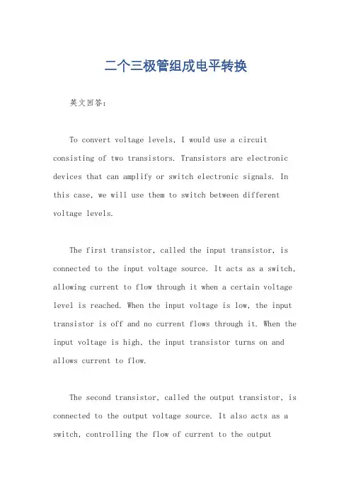
二个三极管组成电平转换英文回答:To convert voltage levels, I would use a circuit consisting of two transistors. Transistors are electronic devices that can amplify or switch electronic signals. In this case, we will use them to switch between different voltage levels.The first transistor, called the input transistor, is connected to the input voltage source. It acts as a switch, allowing current to flow through it when a certain voltage level is reached. When the input voltage is low, the input transistor is off and no current flows through it. When the input voltage is high, the input transistor turns on and allows current to flow.The second transistor, called the output transistor, is connected to the output voltage source. It also acts as a switch, controlling the flow of current to the outputvoltage source. The output transistor is connected to the input transistor in such a way that when the inputtransistor is on, the output transistor is off, and vice versa.By connecting the input and output transistors in this way, we can achieve voltage level conversion. When theinput voltage is low, the input transistor is off, and the output transistor is on, allowing current to flow from the output voltage source. This results in a low output voltage. When the input voltage is high, the input transistor turns on, turning off the output transistor and preventingcurrent from flowing to the output voltage source. This results in a high output voltage.Let me give you an example to illustrate how thiscircuit works. Suppose we have an input voltage of 3V andan output voltage of 5V. When the input voltage is below 3V, the input transistor is off, and the output transistor is on, allowing current to flow from the 5V source. Thisresults in a low output voltage of 0V. When the input voltage is above 3V, the input transistor turns on, turningoff the output transistor and preventing current from flowing to the 5V source. This results in a high output voltage of 5V.中文回答:要实现电平转换,我会使用由两个三极管组成的电路。
逻辑电平转换(英文)Maxim > App Notes > MICROCONTROLLERSKeywords: logic-level translation, MAX1840, MAX1841, MAX3001, MAX3370-MAX3393, MAX8860, MAX8867Jul 21, 2004 APPLICATION NOTE 3007Logic-Level TranslationAbstract: Logic level translation techniques and pitfalls - and Maxim solutions.Electronic design has changed considerably since the days when TTL and 5V CMOS were the dominant standards for logic circuits. The increasing complexity of modern electronic systems has led to lower voltage logic, which in turn can cause incompatibility between input and output levels for the logic families within a system. It is not unusual, for example, that a digital section operating at 1.8V must communicate with an analog subsection operating at 3.3V. This article examines the basics of logic operation and considers,primarily for serial-data systems, the available methods for translating between different domains of logic voltage.The Need for Logic-Level TranslationThe growth of digital ICs that feature incompatible voltage rails, lower V DD rails, or dual rails for V CORE and V I/O has made the translation of logic levels necessary. The use of mixed-signal ICs with lower supply voltages that have not kept pace with those of their digital counterparts also creates the need for logic-level translation. Translation methods vary according to the range of voltages encountered, the number of lines to be translated (e.g., a 4-line Serial Peripheral Interface (SPI?) versus a 32-bit data bus),and the speed of the digital signals. Many logic ICs can translate from high to low levels (such as 5V to 3.3V logic), but fewer can translate from low to high (3.3V to 5V). Level translation can be accomplished with single discrete transistors or even with a resistor-diode combination, but the parasitic capacitance inherent in these methods can reduce the data-transfer rate.Although byte-wide and word-wide level translators are available, they are not optimal for the < 20Mbps serial buses discussed in this article (SPI, I2C, USB, etc.). Thus, translators that require large packages with high pin counts and an I/O-direction pin are not meant for small serial and peripheral interfaces.The Serial Peripheral Interface consists of the unidirectional control lines data in, data out, clock, and chip select. Data in and data out are also known as master in, slave out (MISO) and master out, slave in (MOSI). SPI can be clocked in excess of 20Mbps, and is driven by CMOS push-pull logic. As SPI is unidirectional, translation in both directions on the same signal line is unnecessary. This makes level translation simpler, because you can employ simple techniques involving resistors and diodes (Figure 1) or discrete/digital transistors (Figure 2).Figure 1. A resistor-diode topology is one alternative technique to translation in both directions on the same signal line.Figure 2. Using discrete/digital transistors is another alternative to bidirectional translation.The I2C, SMBus?, and 1-Wire?, interfaces are all bidirectional, open-drain I/O topologies. I2C has three speed ranges: standard mode at ≤ 100kbps, fast mode at ≤ 400kbps, and high-speed mode at ≤ 3.4Mbps. Level translation for bidirectional buses ismore difficult, because one must translate in both directions on the same data line. Simple topologies based on resistor-diode and single-stage-transistor translators with open collector or drain do not work because they are inherently unidirectional.Unidirectional High- to Low-Level Translation—Input Overvoltage ToleranceTo translate from higher to lower logic levels, IC manufacturers produce a range of devices that are said to tolerate overvoltage at their inputs. A logic device is defined as input-overvoltage protected if it can withstand (without damage) an input voltage higher than its supply voltage. Such input-protected devices simplify the task of translating from higher- to lower-V CC logic while increasing the signal-to-noise margin.Overvoltage-tolerant inputs, for example, allow a logic device to cope with logic levels of 1.8V and higher while powered from a 1.8V supply. Devices in the LVC logic family, which are mostly input-overvoltage protected, work well in applications requiring high-to-low translations. The opposite situation of low-to-high translation is not as easy. It may not be feasible to generate higher voltage logic-level thresholds (V IH) from lower voltage logic.When designing a circuit for which connectors, high fanout, or stray load capacitance produce a high capacitance load, you should remember that for all logic families, reducing the supply voltage also decreases the drive capability. An exception occurs between 3.3V CMOS or TTL (LV, LVT, ALVT, LVC, and ALVC) and 5V standard TTL (H, L, S, HS, LS, and ALS). In these logic families, the 3.3V and 5V logic activation points (V OL, V IL, V IH, andV OH) match each other.Mixed High-Low and Low-High TranslationApplications like the SPI bus require a mixture of high-low and low-high translation. Consider, for example, a processor at 1.8V and a peripheral at 3.3V. Though it is possible to mix techniques as described above, a single chip such as the MAX1840, MAX1841, or MAX3390 can implement the necessary translation by itself (Figure 3).Figure 3. This diagram shows an example of an IC level translator with an SPI/QSPI?/MICROWIRE? interface that can implement the necessary mixture of high-low and low-high translation.Other systems, such as I2C and 1-Wire buses, require logic translation in both directions. Simple topologies, based on a single transistor with open collector or drain, do not work in a bidirectional bus because they are inherently unidirectional.Bidirectional Transceiver MethodsFor the larger byte- and word-wide buses where WR and RD signals already exist, one method for transferring data across the voltage levels is a bus switch such as the 74CBTB3384. Such devices are typically optimized for operation between 3.3V and 5V. For smaller 1- and 2-wire buses, this approach raises two issues. Firstly, it requires a separate enable pin to control the direction of data flow, and this ties up valuable port pins. Secondly, it requires large ICs that take up valuable board space.All techniques have their pros and cons. Nonetheless, designers need a universal device that works across all translation levels, enables mixed low-to-high and high-to-low logic transitions, and includes unidirectional and/or bidirectional translation. A next-generation bidirectional level shifter (the MAX3370 in the MAX3370–MAX3393 family of ICs) fulfills those needs while overcoming some of the problems associated withalternative approaches. The MAX3370, which implements a transmission-gate method of level translation (Figure 4), relies on external output drivers to sink current, whether they operate in a low-voltage or higher voltage logic domain. That capability enables the device to work with either open-drain or push-pull output stages. The relatively low on-resistance of a transmission gate (less than 135?), moreover, limits the speed of operation much less than the series resistor of Figure 1.Figure 4. The MAX3370 implements a transmission-gate method of level translation.The design in Figure 4 offers two other advantages. Firstly, for open-drain topologies, the MAX3370 includes10k? pull-up resistors paralleled by a "speed-up" switch. This minimizes the need for external pull-up resistors while reducing the RC time-constant ramp associated with traditional open-drain topologies. Secondly, theMAX3370's tiny SC70 package also conserves valuable board space.Solving the Speed ProblemRC time constants limit the effective data rate for most other open-drain approaches (Figures 5 and 6). The MAX3370 IC family includes a patented speed-up scheme that actively pulls up rising edges, thereby minimizing the effect of capacitive loads as illustrated in Figures 7, 8, and 9. When the input goes above a predefined threshold, the device actively pulls up the rising edge, thereby minimizing any skew caused by external parasitic components. That capability can allow data rates as high as 20Mbps for signals produced by a push-pull driver. The speed of signals from open-drain drivers tends to be slower. As for other open-drain topologies, however,you can improve their speed by adding external pull-up resistors.Figure 5. The scope plot of single FET open-drain output at 20kHz shows a limited effective data rate due to RC time constants.Figure 6. Scope plots of a dual-transistor transceiver translating 1.8V to 5V at 400kHz (a) and at 100kHz (b) illustrate limited effective data rates.Figure 7. A scope plot of MAX3370 output with a translation of 1.8V to 5V at 400kHz shows minimized capacitive load effects.Figure 8. This scope plot of the MAX3370 output at 400kHz with 4.7k?pullup resistors shows the minimized effect of capacitive loads.Figure 9. This plot shows an example of rail-to-rail driving of the output from a MAX3370 high-speed test circuit. Solving the Universal Voltage ProblemAn application ideally requires a single component that can translate between any two logic levels at any speed. The ICs in the MAX337x family are designed for logic levels as low as 1.2V and as high as 5.5V. Consequently, this single component can provide the level translation required in most cases, without needing to select a logic device for each level-translator requirement.Formerly, the need for low-to-high and high-to-low translations in the same circuit could be met only with separate chips. Now the bidirectional and topology-independent features (push-pull or open-drain) of a single chip from the MAX337x family solve both problems. The MAX3370 is a single-line, universal logic-level translator. For translating a larger number of I/O lines, consult the devices listed in Table 1.。
常用的电平转换方案1,TTL电平(什么是TTL电平):输出高电平>2.4V,输出低电平<0.4V。
在室温下,一般输出高电平是3.5V,输出低电平是0.2V。
最小输入高电平和低电平:输入高电平>=2.0V,输入低电平<=0.8V,噪声容限是0.4V。
2,CMOS电平:1逻辑电平电压接近于电源电压,0逻辑电平接近于0V。
而且具有很宽的噪声容限。
3,电平转换电路:因为TTL和COMS的高低电平的值不一样(ttl 5v<==>cmos 3.3v),所以互相连接时需要电平的转换:就是用两个电阻对电平分压,没有什么高深的东西。
哈哈4,OC门,即集电极开路门电路,OD门,即漏极开路门电路,必须外界上拉电阻和电源才能将开关电平作为高低电平用。
否则它一般只作为开关大电压和大电流负载,所以又叫做驱动门电路。
5,TTL和COMS电路比较:1)TTL电路是电流控制器件,而coms电路是电压控制器件。
2)TTL电路的速度快,传输延迟时间短(5-10ns),但是功耗大。
COMS电路的速度慢,传输延迟时间长(25-50n s),但功耗低。
COMS电路本身的功耗与输入信号的脉冲频率有关,频率越高,芯片集越热,这是正常现象。
3)COMS电路的锁定效应:COMS电路由于输入太大的电流,内部的电流急剧增大,除非切断电源,电流一直在增大。
这种效应就是锁定效应。
当产生锁定效应时,COMS的内部电流能达到40mA以上,很容易烧毁芯片。
防御措施:1)在输入端和输出端加钳位电路,使输入和输出不超过不超过规定电压。
2)芯片的电源输入端加去耦电路,防止VDD端出现瞬间的高压。
3)在VDD和外电源之间加线流电阻,即使有大的电流也不让它进去。
4)当系统由几个电源分别供电时,开关要按下列顺序:开启时,先开启COMS电路得电源,再开启输入信号和负载的电源;关闭时,先关闭输入信号和负载的电源,再关闭COMS电路的电源。
6,COMS电路的使用注意事项1)COMS电路时电压控制器件,它的输入总抗很大,对干扰信号的捕捉能力很强。
应用报告ZHCA047–2004年6月选择正确的电平转换解决方案Prasad Dhond摘要电源电压持续迁移到较低的节点以支持当前的低功耗高性能应用。
虽然某些器件可以在较低的电源节点运行,但是其它器件可能不具有这种能力。
为了在这些器件之间实现切换兼容性,每个驱动器的输出必须与其驱动的接收器的输入兼容。
用于实现这些器件的互相连接的电平转换方案有很多。
根据应用的不同需要,某种方法可能比其它方法更适合。
本应用报告概述了用于转换逻辑电平的方法和产品,并列出了每种德州仪器(TI)电平转换解决方案的优缺点。
关键字:双电源、分离轨、电平转换、电平转换器、混合电压、T45、T245、4245、3245、漏极开路、过压容限、TTL、CMOS、TVC、CB3T、CBTD主题页1简介*V CC A not equal to V CC BV CCV CCV CCV CC V CC V CC V OHV IHV TV ILV OL GND5 V 4.44 V0.7 y V CC 0.5 y V CC 0.3 y V CC 0.5 V 0 VV IH V IL GNDV OH V IH V T V IL V IL V OL GND5 V2.4 V 2 V1.5 V 0.8 V0.4 V 0 VV OH V IH V T V OL GND3.3 V2.4 V 2 V 1.5 V 0.8 V 0.4 V 0 V2.5 V 2.0 V 1.7 V0.7 V 0.4 V 0 VV OH V IH V IL V OL GND1.8 V V CC−0.45 V0.65y V CC 0.35y V CC0.45 V0 VV OH V IHV IL V OLGND1.2 V 0.65y V CC 0.35y V CC0 VV CC 1.5 V 0.65y V CC0.35y VCC0 V V IH V IL GND5−V CMOS 5−V TTL 3.3−V LVTTL 2.5−V CMOS 1.8−V CMOS 1.5−V CMOS 1.2−V CMOS2双电源电平转换器简介在目前大多数电子系统中,对电压电平转换的需求非常普遍。
5v转24v 脉冲电平转换电路英文版5V to 24V Pulse Level Conversion CircuitIn electronics, level conversion is a crucial technique that allows different devices or circuits to communicate effectively. One such conversion is the transition from a low voltage level, typically 5V, to a higher voltage level, such as 24V. This process is particularly useful in scenarios where a low-voltage control signal needs to control a high-voltage device or system.The pulse level conversion circuit, specifically designed for this purpose, converts the input pulse signals from a lower voltage to a higher voltage. This conversion is achieved using a combination of transistors, resistors, and capacitors. The transistors act as switches, allowing the circuit to switch between the two voltage levels. The resistors and capacitors control the flow of current and maintain stability in the circuit.In a 5V to 24V pulse level conversion circuit, the input signal, typically a 5V pulse, triggers the transistors to switch on, allowing the flow of current from the higher voltage source (24V) to the output. When the input pulse ends, the transistors switch off, cutting off the flow of current and maintaining the output at the higher voltage level.This conversion circuit is highly efficient and can handle fast pulse signals, making it suitable for various applications such as motor control, relay activation, and other high-voltage systems. It is crucial to design the circuit carefully to ensure reliable and efficient performance.中文版5V转24V脉冲电平转换电路在电子学中,电平转换是一项至关重要的技术,它允许不同的设备或电路进行有效的通信。
nmos的电平转换电路英文回答:NMOS level shifting circuit is a circuit used to convert voltage levels from one logic level to another using NMOS transistors. It is commonly used in digital systems where different voltage levels are used for different logic levels.The basic principle of an NMOS level shifting circuitis to use a pull-up resistor and a NMOS transistor to create a voltage divider. The pull-up resistor is connected between the output and the positive power supply voltage, while the NMOS transistor is connected between the output and ground. By controlling the gate voltage of the NMOS transistor, the output voltage can be shifted to the desired logic level.For example, let's say we have a digital system that operates at 3.3V logic level, but we need to interface itwith another system that operates at 5V logic level. We can use an NMOS level shifting circuit to convert the 3.3Vlogic level to 5V logic level.In this case, we can connect a pull-up resistor between the output and the 5V power supply, and connect an NMOS transistor between the output and ground. By applying a voltage higher than the threshold voltage of the NMOS transistor to its gate, the transistor will turn on andpull the output voltage close to ground, resulting in a logic low level. On the other hand, by applying a voltage lower than the threshold voltage of the NMOS transistor to its gate, the transistor will turn off and the pull-up resistor will pull the output voltage close to the 5V power supply, resulting in a logic high level.This NMOS level shifting circuit allows us to interface the 3.3V logic level system with the 5V logic level system, ensuring proper communication between the two systems.中文回答:NMOS电平转换电路是一种使用NMOS晶体管将电压从一种逻辑电平转换为另一种逻辑电平的电路。
Application ReportSCEA044–June2010A Guide to Voltage Translation With TXS-Type Translators Dave Moon,Aeysha Sultana High Volume LinearABSTRACTModern trends are driving the need for lower supply voltages across many system-level designs.As most processor voltage levels continue to decrease in the interest of achieving the lowest possible power consumption,peripheral devices maintain a need for higher voltage levels,creating potential for voltage discontinuities within a system.To remedy this mixed voltage system incompatibility,a voltage translator can be used.Texas Instruments High Volume Linear group offers a wide-range of voltage level translators.A variety of architectures provide solutions for different application environments including dual-supply direction-controlled,auto-direction sensing,and application-specific memory card interface translators.The information in this application report is intended to help system designers understand the architecture and operation of the TXS-type auto-direction sensing translator familyContents1The Need For Voltage-Level Translation (2)2Auto-Direction Sensing Voltage Translator Architecture (2)3Input Driver Requirements With TXS-Type Translators (6)4Driving External Loads With TXS-Type Translators (7)5Output Enable Control (7)6Conclusion (7)List of Figures1Digital Switching Levels (2)2Basic TXS0101,TXS0102,and TXS0104Architecture (3)3Transfer Characterisitics of an N-Channel Transistor (3)4Basic TXS0108E Architecture (4)5TXS0108E During Low-to-High Signal Transition (5)6TXS0108E During High-to-Low Signal Transition (6)1 SCEA044–June2010A Guide to Voltage Translation With TXS-Type TranslatorsCopyright©2010,Texas Instruments IncorporatedV CCV CCV CC V CC V CC V CC V OH V IH V T V IL V OL GND 5V4.44 V 0.7V CC 0.5V CC 0.3V CC 0.5 V 0 V V IH V IL GND V OH V IHV TV IL V IL V OL GND 5 V 2.4 V2 V 1.5 V 0.8 V 0.4 V 0 V V OH V IH V T V OL GND 3.3 V 2.4 V 2 V 1.5 V 0.8 V 0.4 V 0 V 2.5 V 2.0 V 1.7 V 0.7 V 0.4 V 0 V V OH V IH V ILV OLGND 1.8 V V CC -0.45V 0.65V CC 0.35V CC 0.45V 0 V V OH V IH V IL V OL GND 1.2 V 0.65V CC 0.35V CC 0 V V CC 1.5 V 0.65V CC 0.35V CC 0 V V IH V IL GND5V CMOS 5V TTL 3.3V LVTTL 2.5V CMOS 1.8V CMOS 1.5V CMOS 1.2V CMOSThe Need For Voltage-Level Translation 1The Need For Voltage-Level TranslationThe need for voltage level translation is becoming increasingly significant in today's electronic systems.As the digital switching level standards have continued to progress toward lower voltage levels,systemincompatibilities have arisen.Figure 1illustrates the trend toward lower system voltage levels anddemonstrates the incompatibilities that mixed voltage systems can face.Figure 1.Digital Switching LevelsFor two devices to interface reliably,the output driver voltages must be compatible with receiver inputthresholds.For this condition to be met in mixed voltage systems,a voltage translator is often required.Texas Instruments offers several unique device architectures for addressing voltage translation needs.The most familiar to system designers is probably a direction-controlled buffer translator,such as theSN74AVC8T245.These translators can help remedy many problems in system voltage compatibility but require DIR (direction)control pins.If the system environment does not provide a programmable GPIO to control the direction pin,an auto-direction sensing translator architecture can provide an alternativetranslation solution.2Auto-Direction Sensing Voltage Translator ArchitectureIf a processer GPIO input direction-control signal is not available or if one is not desired,an auto-direction sensing voltage translator can provide a robust solution.As the name implies,this type of translator does not require the use of a direction control signal,and each channel supports independent transmission or reception of data.This eliminates the need for a processor GPIO to control a DIR input,resulting insimplified software driver development as well as smaller device packaging due to reduced pin count.The two types of auto-direction sensing voltage translator architectures are TXB buffered-type and TXS switch-type.Neither type of architecture requires a DIR control signal to establish the direction of dataflow.The TXB translators are designed to exclusively be connected and interfaced with a push-pull drivers and are capable of driving a light capacitive or high impedance loads in applications such as SecureDigital (SD)or Serial Peripheral Interface (SPI).See the TI application report,A Guide to VoltageTranslation With TXB-Type Translators (SCEA043)for more information on the TXB-type voltagetranslators.Texas Instruments has developed several types of TXS-type (where the "S"indicates switch-type)translators that are designed to interface with open-drain drivers and can be used in applications such as I 2C.2A Guide to Voltage Translation With TXS-Type TranslatorsSCEA044–June 2010Copyright ©2010,Texas Instruments IncorporatedV CCA V CCBV (V)IN V = 4.3 VGATE V = 3.5 VGATE V = 2.8 V GATE V = 2.5 VGATE V = 2.2 VGATE V (V )O U T 2.1Initial Series of TXS Type DevicesThe initial series of TXS type devices are the TXS0101,TXS0102,and TXS0104E.The basic blockdiagram architecture of a single-bit (or channel)is shown in Figure 2.Figure 2.Basic TXS0101,TXS0102,and TXS0104ArchitectureThese TXS translators are FET-based architectures that utilize an N-channel pass-gate transistor to open and close the connection between the A-port and B-port.When a driver connected to A or B port is low,the opposite port is,in turn,pulled low by the N2pass-gate transistor.This pass-transistor type voltagetranslator is ideal for down-translation and over-voltage protection.Figure 3shows the transfer characteristics of the N2pass-gate transistor,where the threshold voltage (V T )is approximately 1V and the gate bias voltage (V GATE )is as shown.Figure 3.Transfer Characterisitics of an N-Channel TransistorThe pass-gate transistor,N2,is on when V GS >V T .Consider first the case where one side of N2is held low by an external driver.With the input to N2at 0V,N2will be “On”and the output of N2will be held to nearly 0V due to the on-state resistance of N2.As can be seen in Figure 3,as the input voltage rises due to a rising edge,the output voltage of N2will track the input until of N2turns off at V GATE –V T .After N2stops conducting,the input and output ports will continue to rise to their respective supply voltages due to 3SCEA044–June 2010A Guide to Voltage Translation With TXS-Type TranslatorsCopyright ©2010,Texas Instruments IncorporatedV CCAV CCBthe internal pull-up resistors on either port.Secondly,consider the case where both ports start out high.The ports will be held at static high levels due to the internal pull-up resistors.When the input port ispulled low by an external driver,N2will begin to conduct once V GS >V T .As N2starts to conduct theoutput will begin to track the input port following the curve in the Figure 3.The sinking-current required to perform this translation function must be provided by an external system driver that is connected to either the A or B ports.These pass-transistor voltage translators and their voltage clamping feature makes TXS type translators an ideal choice for applications requiring over-voltage protection and addition to voltage level translation.The signal propagation delay through the N2transistor is extremely fast making it an elegant solution.To achieve faster data rates through the device,these translators include rising edge-rate acceleration circuitry to provide stronger ac-drive by bypassing these integrated 10-k Ωpull-up resistors through a low impedance path during low-to-high signal transitions.A one-shot (O.S.)circuit with an associated T1/T2PMOS transistors is used to increase switching speeds for the rising-edge input signals.When a rising edge is detected by the O.S.circuit,the T1/T2PMOS transistors turn on momentarily to rapidly drive the port high,effectively lowering the output impedance seen on that port and speeding up rising edge inputs.The combination of an N-channel pass FET,integrated 10-k Ωpull-up resistors,and edge-rate acceleration circuits makes the TXS type translators ideal for interfacing devices or systems operating at disparatevoltage levels while also allowing for simple interfacing with open-drain (O.D.)as is required in I 2C,1-wire,and MMC-card interface applications.The TXS0101,TXS0102,and TXS0104E translators also incorporate integrated pull-up resistors andhigher level ESD protection which saves board space and overall BOM cost.TXS-type translators can support push-pull driving applications,and have the ability to drive slightly heavier Impedance loads than the TXB-type translators.However,the TXB-type translators may prove to be a better solution if thecapacitive loading is <70pF.2.2Second Series of TXS Type DevicesThe second series switch-type translator is the TXS0108E semi-buffered type architecture and is targeted for higher speed applications.The basic block diagram of a single-bit (or channel)of this "semi-buffered"translator is shown in Figure 4.Figure 4.Basic TXS0108E Architecture4A Guide to Voltage Translation With TXS-Type TranslatorsSCEA044–June 2010Copyright ©2010,Texas Instruments IncorporatedOne-ShotTranslator1.8V 3.3V V = 1.8 V and V = 3.3 VCCA CCB The design goals for this type of translator were to achieve faster data rates while also providing support for applications where a channel needs to start out in a low-speed open-drain (O.D.)mode,but eventually transition over to a higher-speed push-pull mode.MMC memory card applications are an example of this type of operating mode.The TXS0108E translator reliably supports high-speed data rates in excess of 60Mbps,whereas the initial TXS series type translators supported slightly less than half this.The ability to translate down to the 1.2V operating-node is also supported in the TXS0108E device.To achieve these faster data rates,both rising-edge and falling-edge rate acceleration circuitry isincorporated for symmetrical ac-drive.Again,these accelerators bypass the integrated pull-up resistorsduring low-to-high and high-to-low signal transitions and speed up the output slew rate after monitoring A and B port input rising and falling edges for signal transitions.Figure 4shows the O.S.circuit and itsassociated P1/P2PMOS transistor which are used to improve switching speeds for the rising edge signal by lowering the output impedance seen on that port and speeding up the rising edge rate.Figure 5shows a low-to-high transition.Figure 5.TXS0108E During Low-to-High Signal TransitionThe translator’s T1,OS3and P2element paths are activated when a low-to-high signal is applied at the A port.The OS3edge-rate accelerator facilitates the fast ramping of low-to-high transition of the signal at the output.The pull-up resistors R pua and R pub provide dc-bias to hold the opposite port high when one of the ports is being driven high.During this acceleration phase,the output resistance of the driver is decreased to approximately 50Ω-70Ωto increase the current drive capability of the device.Figure 6shows a high-to-low transition:5SCEA044–June 2010A Guide to Voltage Translation With TXS-Type TranslatorsCopyright ©2010,Texas Instruments IncorporatedOne-Shot TranslatorV = 1.8 V and V = 3.3 VCCA CCB 1.8V 3.3VInput Driver Requirements With TXS-Type Translators Figure 6.TXS0108E During High-to-Low Signal TransitionThe translator’s T1,OS4and N2element paths are activated when a high-to-low signal is applied at the A port.The OS4edge-rate accelerator facilitates the fast ramping of high-to-low transition of the signal at the output.The N-channel pass-gate transistor and resistors R1and R2provide a dc path between ports A and B.They also provide dc-bias to hold the opposite port low when one of the ports is driven low.The TXS0101/2/4translators have fixed 10-k Ωvalue pull-up resistors which provide dc-bias and dccurrent sourcing/drive capabilities to maintain a high.A key feature that was included in the TXS0108E translator to allow it to operate better in SDIO applications is the use of "smart"pull-up resistors.Thisfeature provides lower static power consumption (when the I/Os are passing a low),supports lower VOL values for the same size pass-gate transistor,and helps improve simultaneous switching performance.These smart pull-up resistors dynamically change value based on whether a low or a high is being passed through the I/O line,as follows:•R PUa and R PUb values are 4k Ωwhen the output is driving a high.•R PUa and R PUb values are 40k Ωwhen the output is driving a low.•The I/O goes into High-Z when the device is disabled via the OE pin or by pulling the either V CCA orV CCB to 0V.The series resistance values of R1and R2are 150Ω(typical).The V GATE gate bias voltage of theN-channel pass transistor is again set to a level that optimizes the switch characteristics for maximumdata rate as well as minimal static supply leakage.3Input Driver Requirements With TXS-Type TranslatorsThe continuous dc-current "sinking"capability is determined by the external system-level driver interfaced to the TXS-type translator.For high bandwidth bidirectional SDIO circuit applications,the I/O port needs to quickly change from an input to an output and vice-vera.Therefore,a modest dc-current "sourcing"capability of 100to 200micro-Amps is needed and the smart pullup resistor values determine the sinking capability.The fall time (t fA ,t fB )of a signal depends on the edge rate and output impedance of the external device driving these SDIO lines as well as the capacitive loading on these lines.Similarly,the t pd and max data rates also depend on the output impedance of the external driver.The values for t fA ,t fB ,t pd ,andmaximum data rates specified in the TXS data sheets assume that the output impedance of the external driver is less than 50Ω.6A Guide to Voltage Translation With TXS-Type TranslatorsSCEA044–June 2010Copyright ©2010,Texas Instruments Incorporated Driving External Loads With TXS-Type Translators 4Driving External Loads With TXS-Type TranslatorsThe TXS-type translators were architected for driving high-impedance loads.As such,the O.S.duration has been set to best optimize trade-offs between dynamic current consumption (I CC ),load drivingcapability,and maximum bit-rate considerations.Careful Printed-Circuit-Board (PCB)layout practices with short trace lengths should be followed to avoid excessive capacitive loading.Ensuring proper O.S.triggering will avoid bus contention,output signal oscillations,and other adverse system-level affects.To accomplish this,PCB signal trace-lengths should be kept short enough such that the round trip delay of any reflection is less than the one-shot duration.This improves signal integrity by ensuring that anyreflection sees a low impedance at the source driver.The O.S.circuits have been designed to stay on for 10to 30ns so the maximum capacitance of the lumped load that can be driven also depends reliably also depends directly on this one-shot duration.There is a tradeoff between achieving a maximum data rate and driving heavy capacitive loadssimultaneously.With heavy capacitive loads,the one-shot can time-out before the signal is driven fully to the positive rail.In this scenario,only the pull-up resistors will pull the line high in accordance with its RC time-constant determined by the resistive and capacitive loadings.It is best to avoid this condition bydriving capacitive loads less than 70pF when maximum data rate are desired.With capacitive loading>70pF,the TXS-type devices will still successfully operate at lower data rates.If the application requires an external pullup or pulldown resistor (R pu or R pd )special consideration must be given to the resistor value.It is important to choose a large enough R pu or R pd to ensure adequate V OH and V OL levels at the output port of the translator.To minimize dynamic I CC and the possibility of signal contention,the user should wait for the O.S.circuit to turn-off before applying a signal in the opposite direction.The worst-case duration is equal to the minimum pulse-width number provided in the Timing Requirements section of this data sheet.Once the O.S.istriggered and switched off,both the A and B ports must go to the same state (i.e.both high or both low)for the one-shot to trigger again.In a dc state,the output drivers maintain a low state through the passtransistor.5Output Enable ControlThe TXS devices offer low power consumption of 5to 10µA maximum I CC when the output enable is high.When the output enable is low,the TXS translator buffer is disabled and the outputs are placed intohigh impedance state for increased power savings.The OE input circuit is referenced to the V CCA power supply and when the device is disabled,the pullup resistors are disabled.In addition,current leakage on the A or B ports will be less than ±1m A when the outputs are disabled.If the application does not require output enable control then the OE pin should be tied to the V CCA supply.Leaving OE floating in an indeterminate state can cause undesirable quiescent current to flow in the device which subsequently increases theoverall power dissipation of the device.The outputs are also disabled and put into a high-impedance state under partial power down conditions and this feature is referred to as a V CC isolation feature.If V CCB =0V,the A-port is disabled.Likewise,if V CCA =0V,the B-port is disabled.For the TXS type translators that do not have IEC level ESD protection (i.e.±15-kV Air-Gap and ±8-kV Contact discharge),they are fully specified for partial-power-downapplications using the I OFF feature.This I OFF circuitry disables the outputs,preventing damaging currentbackflow through the device when these devices are powered down.6ConclusionThe TXS translators offer system designers a good solution to remedy mixed-voltage systemincompatibilities when interfacing with open-drain drivers in applications such as I 2C.These translatorseliminate the need for provisioning a GPIO of a processor,since they change the direction of the data flow automatically without the use of a direction control pin.This can simplify software driver development and allows for solutions in smaller packages because of this direction control pin savings.Visit for data sheets for all bit-width TXS translators along with the full line of TexasInstruments voltage translators.7SCEA044–June 2010A Guide to Voltage Translation With TXS-Type TranslatorsCopyright ©2010,Texas Instruments IncorporatedIMPORTANT NOTICETexas Instruments Incorporated and its subsidiaries(TI)reserve the right to make corrections,modifications,enhancements,improvements, and other changes to its products and services at any time and to discontinue any product or service without notice.Customers should obtain the latest relevant information before placing orders and should verify that such information is current and complete.All products are sold subject to TI’s terms and conditions of sale supplied at the time of order acknowledgment.TI warrants performance of its hardware products to the specifications applicable at the time of sale in accordance with TI’s standard warranty.Testing and other quality control techniques are used to the extent TI deems necessary to support this warranty.Except where mandated by government requirements,testing of all parameters of each product is not necessarily performed.TI assumes no liability for applications assistance or customer product design.Customers are responsible for their products and applications using TI components.To minimize the risks associated with customer products and applications,customers should provide adequate design and operating safeguards.TI does not warrant or represent that any license,either express or implied,is granted under any TI patent right,copyright,mask work right, or other TI intellectual property right relating to any combination,machine,or process in which TI products or services are rmation published by TI regarding third-party products or services does not constitute a license from TI to use such products or services or a warranty or endorsement e of such information may require a license from a third party under the patents or other intellectual property of the third party,or a license from TI under the patents or other intellectual property of TI.Reproduction of TI information in TI data books or data sheets is permissible only if reproduction is without alteration and is accompanied by all associated warranties,conditions,limitations,and notices.Reproduction of this information with alteration is an unfair and deceptive business practice.TI is not responsible or liable for such altered rmation of third parties may be subject to additional restrictions.Resale of TI products or services with statements different from or beyond the parameters stated by TI for that product or service voids all express and any implied warranties for the associated TI product or service and is an unfair and deceptive business practice.TI is not responsible or liable for any such statements.TI products are not authorized for use in safety-critical applications(such as life support)where a failure of the TI product would reasonably be expected to cause severe personal injury or death,unless officers of the parties have executed an agreement specifically governing such use.Buyers represent that they have all necessary expertise in the safety and regulatory ramifications of their applications,and acknowledge and agree that they are solely responsible for all legal,regulatory and safety-related requirements concerning their products and any use of TI products in such safety-critical applications,notwithstanding any applications-related information or support that may be provided by TI.Further,Buyers must fully indemnify TI and its representatives against any damages arising out of the use of TI products in such safety-critical applications.TI products are neither designed nor intended for use in military/aerospace applications or environments unless the TI products are specifically designated by TI as military-grade or"enhanced plastic."Only products designated by TI as military-grade meet military specifications.Buyers acknowledge and agree that any such use of TI products which TI has not designated as military-grade is solely at the Buyer's risk,and that they are solely responsible for compliance with all legal and regulatory requirements in connection with such use. TI products are neither designed nor intended for use in automotive applications or environments unless the specific TI products are designated by TI as compliant with ISO/TS16949requirements.Buyers acknowledge and agree that,if they use any non-designated products in automotive applications,TI will not be responsible for any failure to meet such requirements.Following are URLs where you can obtain information on other Texas Instruments products and application solutions:Products ApplicationsAmplifiers Audio /audioData Converters Automotive /automotiveDLP®Products Communications and /communicationsTelecomDSP Computers and /computersPeripheralsClocks and Timers /clocks Consumer Electronics /consumer-appsInterface Energy /energyLogic Industrial /industrialPower Mgmt Medical /medicalMicrocontrollers Security /securityRFID Space,Avionics&/space-avionics-defenseDefenseRF/IF and ZigBee®Solutions /lprf Video and Imaging /videoWireless /wireless-appsMailing Address:Texas Instruments,Post Office Box655303,Dallas,Texas75265Copyright©2010,Texas Instruments Incorporated。