
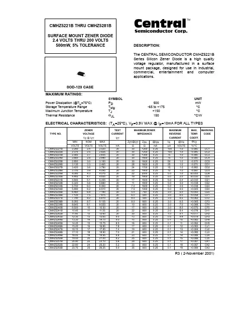
CMHZ5223B中文资料
- 格式:pdf
- 大小:60.04 KB
- 文档页数:2
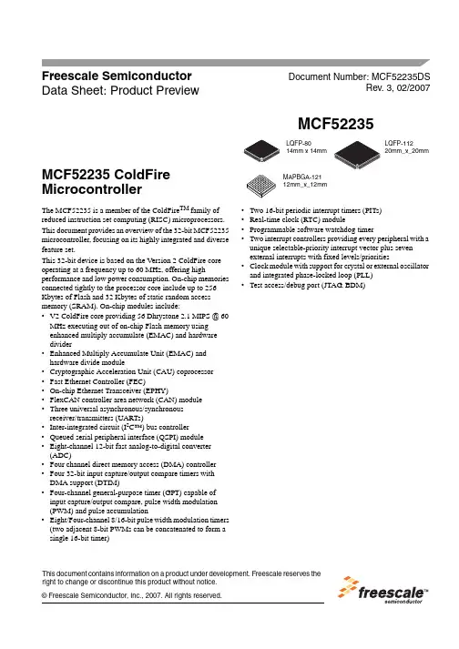
Freescale Semiconductor Data Sheet: Product PreviewDocument Number: MCF52235DSRev. 3, 02/2007This document contains information on a product under development. F reescale reserves the right to change or discontinue this product without notice.MCF52235The MCF52235 is a member of the ColdFire TM family of reduced instruction set computing (RISC) microprocessors.This document provides an overview of the 32-bit MCF52235 microcontroller, focusing on its highly integrated and diverse feature set.This 32-bit device is based on the Version 2 ColdFire core operating at a frequency up to 60 MHz, offering highperformance and low power consumption. On-chip memories connected tightly to the processor core include up to 256 Kbytes of Flash and 32 Kbytes of static random access memory (SRAM). On-chip modules include:•V2 ColdFire core providing 56 Dhrystone 2.1 MIPS @ 60 MHz executing out of on-chip Flash memory using enhanced multiply accumulate (EMAC) and hardware divider•Enhanced Multiply Accumulate Unit (EMAC) and hardware divide module•Cryptographic Acceleration Unit (CAU) coprocessor •Fast Ethernet Controller (FEC)•On-chip Ethernet Transceiver (EPHY)•FlexCAN controller area network (CAN) module •Three universal asynchronous/synchronous receiver/transmitters (UARTs)•Inter-integrated circuit (I 2C™) bus controller •Queued serial peripheral interface (QSPI) module •Eight-channel 12-bit fast analog-to-digital converter (ADC)•Four channel direct memory access (DMA) controller •Four 32-bit input capture/output compare timers with DMA support (DTIM)•Four-channel general-purpose timer (GPT) capable of input capture/output compare, pulse width modulation (PWM) and pulse accumulation•Eight/Four-channel 8/16-bit pulse width modulation timers (two adjacent 8-bit PWMs can be concatenated to form a single 16-bit timer)•Two 16-bit periodic interrupt timers (PITs)•Real-time clock (RTC) module•Programmable software watchdog timer•Two interrupt controllers providing every peripheral with a unique selectable-priority interrupt vector plus seven external interrupts with fixed levels/priorities•Clock module with support for crystal or external oscillator and integrated phase-locked loop (PLL)•Test access/debug port (JTAG, BDM)MCF52235 ColdFire MicrocontrollerTable of Contents1MCF52235 Family Configurations . . . . . . . . . . . . . . . . . . . . . .31.1Block Diagram. . . . . . . . . . . . . . . . . . . . . . . . . . . . . . . . .31.2Features . . . . . . . . . . . . . . . . . . . . . . . . . . . . . . . . . . . . .41.3Package Pinouts. . . . . . . . . . . . . . . . . . . . . . . . . . . . . .131.4Reset Signals . . . . . . . . . . . . . . . . . . . . . . . . . . . . . . . .211.5PLL and Clock Signals . . . . . . . . . . . . . . . . . . . . . . . . .211.6Mode Selection. . . . . . . . . . . . . . . . . . . . . . . . . . . . . . .211.7External Interrupt Signals. . . . . . . . . . . . . . . . . . . . . . .211.8Queued Serial Peripheral Interface (QSPI). . . . . . . . . .221.9Fast Ethernet Controller EPHY Signals . . . . . . . . . . . .221.10I2C I/O Signals . . . . . . . . . . . . . . . . . . . . . . . . . . . . . . .231.11UART Module Signals. . . . . . . . . . . . . . . . . . . . . . . . . .231.12DMA Timer Signals. . . . . . . . . . . . . . . . . . . . . . . . . . . .231.13ADC Signals . . . . . . . . . . . . . . . . . . . . . . . . . . . . . . . . .241.14General Purpose Timer Signals . . . . . . . . . . . . . . . . . .241.15Pulse Width Modulator Signals. . . . . . . . . . . . . . . . . . .241.16Debug Support Signals. . . . . . . . . . . . . . . . . . . . . . . . .241.17EzPort Signal Descriptions. . . . . . . . . . . . . . . . . . . . . .261.18Power and Ground Pins . . . . . . . . . . . . . . . . . . . . . . . .26 2Preliminary Electrical Characteristics. . . . . . . . . . . . . . . . . . .272.1Maximum Ratings. . . . . . . . . . . . . . . . . . . . . . . . . . . . .282.2ESD Protection. . . . . . . . . . . . . . . . . . . . . . . . . . . . . . .302.3DC Electrical Specifications . . . . . . . . . . . . . . . . . . . . .312.4Phase Lock Loop Electrical Specifications. . . . . . . . . .322.5General Purpose I/O Timing. . . . . . . . . . . . . . . . . . . . .342.6Reset Timing. . . . . . . . . . . . . . . . . . . . . . . . . . . . . . . . .352.7I2C Input/Output Timing Specifications. . . . . . . . . . . . .352.8EPHY Timing . . . . . . . . . . . . . . . . . . . . . . . . . . . . . . . .372.9Analog-to-Digital Converter (ADC) Parameters . . . . . .372.10DMA Timers Timing Specifications. . . . . . . . . . . . . . . .392.11QSPI Electrical Specifications. . . . . . . . . . . . . . . . . . . .392.12JTAG and Boundary Scan Timing. . . . . . . . . . . . . . . . .402.13Debug AC Timing Specifications. . . . . . . . . . . . . . . . . .42 3Mechanical Outline Drawings. . . . . . . . . . . . . . . . . . . . . . . . .433.180-pin LQFP Package. . . . . . . . . . . . . . . . . . . . . . . . . .433.2112-pin LQFP Package. . . . . . . . . . . . . . . . . . . . . . . . .443.3121 MAPBGA Package. . . . . . . . . . . . . . . . . . . . . . . . .47 4Revision History . . . . . . . . . . . . . . . . . . . . . . . . . . . . . . . . . . .49 List of FiguresFigure1.MCF52235 Block Diagram . . . . . . . . . . . . . . . . . . . . . . 4 Figure2.80-pin LQFP Pin Assignments . . . . . . . . . . . . . . . . . . 13 Figure3.112-pin LQFP Pin Assignments . . . . . . . . . . . . . . . . . 14 Figure4.121 MAPBGA Pin Assignments . . . . . . . . . . . . . . . . . 15 Figure5.Suggested Connection Scheme for Power and Ground 27 Figure6.GPIO Timing. . . . . . . . . . . . . . . . . . . . . . . . . . . . . . . . 34 Figure7.RSTI and Configuration Override Timing . . . . . . . . . . 35 Figure8.I2C Input/Output Timings . . . . . . . . . . . . . . . . . . . . . . 36 Figure9.EPHY Timing . . . . . . . . . . . . . . . . . . . . . . . . . . . . . . . 37Figure10.Equivalent Circuit for A/D Loading. . . . . . . . . . . . . . . 39 Figure11.QSPI Timing. . . . . . . . . . . . . . . . . . . . . . . . . . . . . . . . 40 Figure12.T est Clock Input Timing . . . . . . . . . . . . . . . . . . . . . . . 41 Figure13.Boundary Scan (JTAG) Timing . . . . . . . . . . . . . . . . . 41 Figure14.T est Access Port Timing . . . . . . . . . . . . . . . . . . . . . . 41 Figure15.TRST Timing . . . . . . . . . . . . . . . . . . . . . . . . . . . . . . . 41 Figure16.Real-Time Trace AC Timing. . . . . . . . . . . . . . . . . . . . 42 Figure17.BDM Serial Port AC Timing. . . . . . . . . . . . . . . . . . . . 42 List of TablesT able1.MCF52235 Family Configurations. . . . . . . . . . . . . . . . . 3 T able2.Part Number Summary . . . . . . . . . . . . . . . . . . . . . . . . 13 T able3.Pin Functions by Primary and Alternate Purpose . . . . 16 T able4.Reset Signals . . . . . . . . . . . . . . . . . . . . . . . . . . . . . . . 21 T able5.PLL and Clock Signals . . . . . . . . . . . . . . . . . . . . . . . . 21 T able6.Mode Selection Signals. . . . . . . . . . . . . . . . . . . . . . . . 21 T able7.External Interrupt Signals . . . . . . . . . . . . . . . . . . . . . . 21 T able8.Queued Serial Peripheral Interface (QSPI) Signals. . . 22 T able9.Fast Ethernet Controller (FEC) Signals. . . . . . . . . . . . 22 T able10.I2C I/O Signals. . . . . . . . . . . . . . . . . . . . . . . . . . . . . . . 23 T able11.UART Module Signals. . . . . . . . . . . . . . . . . . . . . . . . . 23 T able12.DMA Timer Signals . . . . . . . . . . . . . . . . . . . . . . . . . . . 23 T able13.ADC Signals . . . . . . . . . . . . . . . . . . . . . . . . . . . . . . . . 24 T able14.GPT Signals . . . . . . . . . . . . . . . . . . . . . . . . . . . . . . . . 24 T able15.PWM Signals. . . . . . . . . . . . . . . . . . . . . . . . . . . . . . . . 24 T able16.Debug Support Signals . . . . . . . . . . . . . . . . . . . . . . . . 24 T able17.EzPort Signal Descriptions . . . . . . . . . . . . . . . . . . . . . 26 T able18.Power and Ground Pins. . . . . . . . . . . . . . . . . . . . . . . . 26 T able19.Absolute Maximum Ratings, . . . . . . . . . . . . . . . . . . . 28 T able20.Thermal Characteristics. . . . . . . . . . . . . . . . . . . . . . . . 28 T able21.ESD Protection Characteristics, . . . . . . . . . . . . . . . . . 30 T able22.DC Electrical Specifications . . . . . . . . . . . . . . . . . . . . 31 T able23.Active Current Consumption Specifications. . . . . . . . . 32 T able24.Current Consumption Specificationsin Low-Power Modes. . . . . . . . . . . . . . . . . . . . . . . . . . 32 T able25.PLL Electrical Specifications. . . . . . . . . . . . . . . . . . . . 32 T able26.GPIO Timing . . . . . . . . . . . . . . . . . . . . . . . . . . . . . . . . 34 T able27.Reset and Configuration Override Timing. . . . . . . . . . 35 T able28.I2C Input Timing Specifications betweenI2C_SCL and I2C_SDA. . . . . . . . . . . . . . . . . . . . . . . . 35 T able29. I2C Output Timing Specifications betweenI2C_SCL and I2C_SDA. . . . . . . . . . . . . . . . . . . . . . . . 36 T able30.EPHY Timing. . . . . . . . . . . . . . . . . . . . . . . . . . . . . . . . 37 T able31.ADC Parameters . . . . . . . . . . . . . . . . . . . . . . . . . . . . . 37 T able32.Timer Module AC Timing Specifications . . . . . . . . . . . 39 T able33.QSPI Modules AC Timing Specifications. . . . . . . . . . . 39 T able34.JT AG and Boundary Scan Timing. . . . . . . . . . . . . . . . 40 T able35.Debug AC Timing Specification. . . . . . . . . . . . . . . . . . 42 T able36.Revision History. . . . . . . . . . . . . . . . . . . . . . . . . . . . . . 49MCF52235 Family Configurations1MCF52235 Family ConfigurationsTable 1. MCF52235 Family ConfigurationsModule5223052231522335223452235ColdFire Version 2 Core with EMAC (Enhanced Multiply-Accumulate Unit)•••••System Clock60MHz Performance (Dhrystone 2.1 MIPS)56Flash / Static RAM (SRAM)128/32Kbytes 128/32Kbytes256/32KbytesInterrupt Controllers (INTC0/INTC1)•••••Fast Analog-to-Digital Converter (ADC)•••••Random Number Generator and Crypto Acceleration Unit (CAU)————•FlexCAN 2.0B Module—•—••Fast Ethernet Controller (FEC) with on-chip interface (EPHY)•••••Four-channel Direct-Memory Access (DMA)•••••Software Watchdog Timer (WDT)•••••Programmable Interrupt Timer 22222Four-Channel General Purpose Timer •••••32-bit DMATimers 44444QSPI •••••UART(s)33333I 2C•••••Eight/Four-channel 8/16-bit PWM Timer •••••General Purpose I/O Module (GPIO)•••••Chip Configuration and Reset Controller Module •••••Background Debug Mode (BDM)•••••JT AG - IEEE 1149.1 Test Access Port 11The full debug/trace interface is available only on the 112- and 121-pin packages. A reduced debug interface is bonded on the80-pin package.•••••Package80, 112-pin LQFP80, 112-pin LQFP80, 112-pin LQFP 112-pin LQFP 121 MAPBGA 112-pin LQFP 121 MAPBGAMCF52235 Family Configurations1.1Block DiagramThe MCF52235 (or its variants) comes in 80- and 112-pin low-profile quad flat pack packages (LQFP) and a 121 MAPBGA, and operates in single-chip mode only. Figure 1 shows a top-level block diagram of the MCF52235.Figure 1. MCF52235 Block Diagram1.2FeaturesThis document contains information on a new product under development. Freescale reserves the right to change or discontinue this product without notice. Specifications and information herein are subject to change without notice.ArbiterInterrupt Controller 1UART 0QSPIUART 1UART 2I 2CDTIM 0DTIM 1DTIM 2DTIM 3V2 ColdFire CPUIFPOEPEMAC4 CH DMA MUXJTAG TAPTo/From PADI32 Kbytes SRAM (4K ×16)×4256 Kbytes Flash (32K ×16)×4PORTS (GPIO)CIMRSTIN RSTOUTSDA SCL UTXD n URXD n URTS n DTIN n /DTOUT n CANRX JTAG_EN ADCAN[7:0]V RH V RLPLL CLKGENEdge Port 2FlexCAN EXTAL XTAL CLKOUTRNGA PIT1GPTPWMTo/From Interrupt ControllerCANTX UCTS n PMMP A D I – P i n M u x i n gEzPortEzPCSQSPI_CLK,QSPI_CS n PWM nQSPI_DIN,QSPI_DOUT GPT nFast EthernetController(FEC)EPHY EPHY_RX EPHY_TX PIT0Edge Port 1Interrupt Controller 2EzPQEzPD EzPCK RTCCAUMCF52235 Family Configurations 1.2.1Feature OverviewThe MCF52235 family includes the following features:•Version 2 ColdFire variable-length RISC processor core—Static operation—32-bit address and data paths on-chip—Up to 60MHz processor core frequency—Sixteen general-purpose, 32-bit data and address registers—Implements ColdFire ISA_A with extensions to support the user stack pointer register and four new instructions for improved bit processing (ISA_A+)—Enhanced Multiply-Accumulate (EMAC) unit with 32-bit accumulator to support 16×16→32 or 32×32→32 operations—Cryptography Acceleration Unit (CAU)–Tightly-coupled coprocessor to accelerate software-based encryption and message digest functions–FIPS-140 compliant random number generator—Support for DES, 3DES, AES, MD5, and SHA-1 algorithms—Illegal instruction decode that allows for 68K emulation support•System debug support—Real time trace for determining dynamic execution path—Background debug mode (BDM) for in-circuit debugging (DEBUG_B+)—Real time debug support, with six hardware breakpoints (4 PC, 1 address and 1 data) that can be configured intoa 1- or 2-level trigger•On-chip memories—32-Kbyte dual-ported SRAM on CPU internal bus, supporting core and DMA access with standby power supply support—256 Kbytes of interleaved Flash memory supporting 2-1-1-1 accesses•Power management—Fully static operation with processor sleep and whole chip stop modes—Rapid response to interrupts from the low-power sleep mode (wake-up feature)—Clock enable/disable for each peripheral when not used•Fast Ethernet Controller (FEC)—10/100 BaseT/TX capability, half duplex or full duplex—On-chip transmit and receive FIFOs—Built-in dedicated DMA controller—Memory-based flexible descriptor rings•On-chip Ethernet Transceiver (EPHY)—Digital adaptive equalization—Supports auto-negotiation—Baseline wander correction—Full-/Half-duplex support in all modes—Loopback modes—Supports MDIO preamble suppression—Jumbo packet•FlexCAN 2.0B moduleMCF52235 Family Configurations—Based on and includes all existing features of the Freescale TouCAN module—Full implementation of the CAN protocol specification version 2.0B–Standard Data and Remote Frames (up to 109 bits long)–Extended Data and Remote Frames (up to 127 bits long)–0–8 bytes data length–Programmable bit rate up to 1 Mbit/sec—Flexible Message Buffers (MBs), totalling up to 16 message buffers of 0–8 byte data length each, configurable as Rx or Tx, all supporting standard and extended messages—Unused Message Buffer space can be used as general purpose RAM space—Listen only mode capability—Content-related addressing—No read/write semaphores required—Three programmable mask registers: global for MBs 0-13, special for MB14, and special for MB15—Programmable transmit-first scheme: lowest ID or lowest buffer number—Time stamp based on 16-bit free-running timer—Global network time, synchronized by a specific message—Maskable interrupts•Three universal asynchronous/synchronous receiver transmitters (UARTs)—16-bit divider for clock generation—Interrupt control logic with maskable interrupts—DMA support—Data formats can be 5, 6, 7 or 8 bits with even, odd or no parity—Up to 2 stop bits in 1/16 increments—Error-detection capabilities—Modem support includes request-to-send (RTS) and clear-to-send (CTS) lines for two UARTs—Transmit and receive FIFO buffers•I2C module—Interchip bus interface for EEPROMs, LCD controllers, A/D converters, and keypads—Fully compatible with industry-standard I2C bus—Master and slave modes support multiple masters—Automatic interrupt generation with programmable level•Queued serial peripheral interface (QSPI)—Full-duplex, three-wire synchronous transfers—Up to four chip selects available—Master mode operation only—Programmable bit rates up to half the CPU clock frequency—Up to 16 pre-programmed transfers•Fast analog-to-digital converter (ADC)—Eight analog input channels—12-bit resolution—Minimum 1.125 μs conversion time—Simultaneous sampling of two channels for motor control applications—Single-scan or continuous operation—Optional interrupts on conversion complete, zero crossing (sign change), or under/over low/high limit—Unused analog channels can be used as digital I/OMCF52235 Family Configurations•Four 32-bit DMA timers—17-ns resolution at 60 MHz—Programmable sources for clock input, including an external clock option—Programmable prescaler—Input capture capability with programmable trigger edge on input pin—Output compare with programmable mode for the output pin—Free run and restart modes—Maskable interrupts on input capture or output compare—DMA trigger capability on input capture or output compare•Four-channel general purpose timers—16-bit architecture—Programmable prescaler—Output pulse widths variable from microseconds to seconds—Single 16-bit input pulse accumulator—Toggle-on-overflow feature for pulse-width modulator (PWM) generation—One dual-mode pulse accumulation channel•Pulse-width modulation timer—Operates as eight channels with 8-bit resolution or four channels with 16-bit resolution—Programmable period and duty cycle—Programmable enable/disable for each channel—Software selectable polarity for each channel—Period and duty cycle are double buffered. Change takes effect when the end of the current period is reached (PWM counter reaches zero) or when the channel is disabled.—Programmable center or left aligned outputs on individual channels—Four clock sources (A, B, SA, and SB) provide for a wide range of frequencies—Emergency shutdown•Real-Time Clock (RTC)—Maintains system time-of-day clock—Provides stopwatch and alarm interrupt functions•Two periodic interrupt timers (PITs)—16-bit counter—Selectable as free running or count down•Software watchdog timer—32-bit counter—Low power mode support•Clock Generation Features—25 MHz crystal input—On-chip PLL can generate core frequencies up to maximum 60MHz operating frequency—Provides clock for integrated EPHY•Dual Interrupt Controllers (INTC0/INTC1)—Support for multiple interrupt sources organized as follows:–Fully-programmable interrupt sources for each peripheral–7 fixed-level interrupt sources–Seven external interrupt signalsMCF52235 Family Configurations—Unique vector number for each interrupt source—Ability to mask any individual interrupt source or all interrupt sources (global mask-all)—Support for hardware and software interrupt acknowledge (IACK) cycles—Combinatorial path to provide wake-up from low power modes•DMA controller—Four fully programmable channels—Dual-address transfer support with 8-, 16-, and 32-bit data capability, along with support for 16-byte (4 x 32-bit) burst transfers—Source/destination address pointers that can increment or remain constant—24-bit byte transfer counter per channel—Auto-alignment transfers supported for efficient block movement—Bursting and cycle steal support—Software-programmable DMA requesters for the UARTs (3) and 32-bit timers (4)•Reset—Separate reset in and reset out signals—Seven sources of reset:–Power-on reset (POR)–External–Software–Watchdog–Loss of clock–Loss of lock–Low-voltage detection (LVD)—Status flag indication of source of last reset•Chip integration module (CIM)—System configuration during reset—Selects one of three clock modes—Configures output pad drive strength—Unique part identification number and part revision number•General purpose I/O interface—Up to 56 bits of general purpose I/O—Bit manipulation supported via set/clear functions—Programmable drive strengths—Unused peripheral pins may be used as extra GPIO•JTAG support for system level board testing1.2.2V2 Core OverviewThe version 2 ColdFire processor core is comprised of two separate pipelines decoupled by an instruction buffer. The two-stage instruction fetch pipeline (IFP) is responsible for instruction-address generation and instruction fetch. The instruction buffer is a first-in-first-out (FIFO) buffer that holds prefetched instructions awaiting execution in the operand execution pipeline (OEP). The OEP includes two pipeline stages. The first stage decodes instructions and selects operands (DSOC); the second stage (AGEX) performs instruction execution and calculates operand effective addresses, if needed.The V2 core implements the ColdFire instruction set architecture revision A+ with added support for a separate user stack pointer register and four new instructions to assist in bit processing. Additionally, the MCF52235 core includes the enhanced multiply-accumulate (EMAC) unit for improved signal processing capabilities. The EMAC implements a three-stage arithmeticMCF52235 Family Configurations pipeline, optimized for 16×16 bit operations, with support for one 32-bit accumulator. Supported operands include 16- and 32-bit signed and unsigned integers, signed fractional operands, and a complete set of instructions to process these data types. The EMAC provides support for execution of DSP operations within the context of a single processor at a minimal hardware cost.1.2.3Integrated Debug ModuleThe ColdFire processor core debug interface is provided to support system debugging in conjunction with low-cost debug and emulator development tools. Through a standard debug interface, access debug information and real-time tracing capability is provided on 112-and 121-lead packages. This allows the processor and system to be debugged at full speed without the need for costly in-circuit emulators.The on-chip breakpoint resources include a total of nine programmable 32-bit registers: an address and an address mask register, a data and a data mask register, four PC registers, and one PC mask register. These registers can be accessed through the dedicated debug serial communication channel or from the processor’s supervisor mode programming model. The breakpoint registers can be configured to generate triggers by combining the address, data, and PC conditions in a variety of single- or dual-level definitions. The trigger event can be programmed to generate a processor halt or initiate a debug interrupt exception. The MCF52235 implements revision B+ of the ColdFire Debug Architecture.The MCF52235’s interrupt servicing options during emulator mode allow real-time critical interrupt service routines to be serviced while processing a debug interrupt event, thereby ensuring that the system continues to operate even during debugging. To support program trace, the V2 debug module provides processor status (PST[3:0]) and debug data (DDATA[3:0]) ports. These buses and the PSTCLK output provide execution status, captured operand data, and branch target addresses defining processor activity at the CPU’s clock rate. The MCF52235 includes a new debug signal, ALLPST. This signal is the logical AND of the processor status (PST[3:0]) signals and is useful for detecting when the processor is in a halted state (PST[3:0] = 1111).The full debug/trace interface is available only on the 112 and 121-pin packages. However, every product features the dedicated debug serial communication channel (DSI, DSO, DSCLK) and the ALLPST signal.1.2.4JTAGThe MCF52235 supports circuit board test strategies based on the Test Technology Committee of IEEE and the Joint Test Action Group (JTAG). The test logic includes a test access port (TAP) consisting of a 16-state controller, an instruction register, and three test registers (a 1-bit bypass register, a 256-bit boundary-scan register, and a 32-bit ID register). The boundary scan register links the device’s pins into one shift register. Test logic, implemented using static logic design, is independent of the device system logic.The MCF52235 implementation can do the following:•Perform boundary-scan operations to test circuit board electrical continuity•Sample MCF52235 system pins during operation and transparently shift out the result in the boundary scan register •Bypass the MCF52235 for a given circuit board test by effectively reducing the boundary-scan register to a single bit •Disable the output drive to pins during circuit-board testing•Drive output pins to stable levels1.2.5On-Chip Memories1.2.5.1SRAMThe dual-ported SRAM module provides a general-purpose 32-Kbyte memory block that the ColdFire core can access in a single cycle. The location of the memory block can be set to any 32-Kbyte boundary within the 4-Gbyte address space. This memory is ideal for storing critical code or data structures and for use as the system stack. Because the SRAM module isMCF52235 Family Configurationsphysically connected to the processor's high-speed local bus, it can quickly service core-initiated accesses ormemory-referencing commands from the debug module.The SRAM module is also accessible by the DMA. The dual-ported nature of the SRAM makes it ideal for implementing applications with double-buffer schemes, where the processor and a DMA device operate in alternate regions of the SRAM to maximize system performance.1.2.5.2FlashThe ColdFire flash module (CFM) is a non-volatile memory (NVM) module that connects to the processor’s high-speed local bus. The CFM is constructed with four banks of 32K×16-bit flash arrays to generate 256Kbytes of 32-bit flash memory. These arrays serve as electrically erasable and programmable, non-volatile program and data memory. The flash memory is ideal for program and data storage for single-chip applications, allowing for field reprogramming without requiring an external high voltage source. The CFM interfaces to the ColdFire core through an optimized read-only memory controller which supports interleaved accesses from the 2-cycle flash arrays. A backdoor mapping of the flash memory is used for all program, erase, and verify operations, as well as providing a read datapath for the DMA. Flash memory may also be programmed via the EzPort, which is a serial flash programming interface that allows the flash to be read, erased and programmed by an external controller in a format compatible with most SPI bus flash memory chips. This allows easy device programming via Automated Test Equipment or bulk programming tools.1.2.6Cryptography Acceleration UnitThe MCF52235 device incorporates two hardware accelerators for cryptographic functions. First, the CAU is a coprocessor tightly-coupled to the V2 ColdFire core that implements a set of specialized operations to increase the throughput of software-based encryption and message digest functions, specifically the DES, 3DES, AES, MD5 and SHA-1 algorithms. Second, a random number generator provides FIPS-140 compliant 32-bit values to security processing routines. Both modules supply critical acceleration to software-based cryptographic algorithms at a minimal hardware cost.1.2.7Power ManagementThe MCF52235 incorporates several low-power modes of operation which are entered under program control and exited by several external trigger events. An integrated power-on reset (POR) circuit monitors the input supply and forces an MCU reset as the supply voltage rises. The low voltage detector (LVD) monitors the supply voltage and is configurable to force a reset or interrupt condition if it falls below the LVD trip point.1.2.8FlexCANThe FlexCAN module is a communication controller implementing version 2.0 of the CAN protocol parts A and B. The CAN protocol can be used as an industrial control serial data bus, meeting the specific requirements of reliable operation in a harsh EMI environment with high bandwidth. This instantiation of FlexCAN has 16 message buffers.1.2.9UARTsThe MCF52235 has three full-duplex UARTs that function independently. The three UARTs can be clocked by the system bus clock, eliminating the need for an external clock source. On smaller packages, the third UART is multiplexed with other digital I/O functions.。


SMC522PS/2光电3D鼠标控制芯片SMC5221.概述SMC522是一款性能优良的PS/2光电3D鼠标控制芯片,可与PAN101B204/208系列、ADNS-2051系列配对使用构成高性能光电鼠标。
SMC522采用MICRO控制接口,可使鼠标的解析度400CPI/800CPI动态切换并适用于PS/2 2D 3KEY、PS/2 3D 3KEY、PS/2 3D 5KEY等多种工作模式(根据不同的系统及驱动程序自动切换)。
当工作于3D 3KEY模式时,其第4(Forward)、5(Back)两键相当于中间键。
2.主要特点● 与IBM PS/2 Mouse及Microsoft IntelliMouse完全兼容● 包括IBM PS/2 Mouse规格内的所有指令、回应、状态、错误处理等,毫无删减● PS/2 Mouse的同步串列传输时序精准,与各厂牌IBM PC相容型电脑的相容性最高● 采用MICRO控制接口,可使鼠标的解析度400CPI/800CPI动态切换● 兼容多种光电传感器● 兼容PS/2 2D 3KEY、PS/2 3D 3KEY、PS/2 3D 5KEY等多种工作模式● 仅须外接一个电阻组成RC振荡器,振荡频率8MHz● 外部的零件已减到最少,有效降低生产装配成本● 滚轮为除2设计,适合一般的编码器设计,同时也支持光学滚轮3.管脚排列4.管脚功能说明编号 引脚名 方向 功能描述1 Z1 I 侦测滚轮翻动的光耦或编码器输入2 PS_CLK I/O 与电脑做同步串行传输的CLK讯号线3 PS_DATA I/O 与电脑做同步串行传输的DATA讯号线4 GND - 地5 R I 鼠标右键的输入6 M I 鼠标中间键的输入7 L I 鼠标左键的输入8 FORWARD I 鼠标第4个键(Forward)的输入 9 BACK I 鼠标第5个键(Back)的输入10 PD/ICSel I Power_down 同步/IC 选择(上电时,悬空为选择PAN101B204/208,接下拉电阻选择ADNS-2051)11 SCLK/RESModeI/O 与PAN101B204/208、ADNS-2051通信的时钟线/解析度选择(工作中,悬空为800CPI,接下拉电阻为400CPI) 12 SDIO I/O 与PAN101B204/208、ADNS-2051通信的数据线 13 VDD -5V 电源 14 OSCOUT O 振荡输出 15 OSCIN I 振荡输入16 Z2I侦测滚轮翻动的光耦或编码器输入5.功能详述功能详述5.1 5.1 配置配置配置本产品主要采用Micro 控制方式,可以达到800CPI 的高性能。