
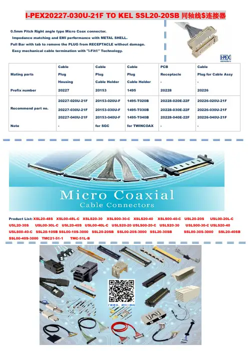
I-PEX20227-030U-21F TO KEL SSL20-20SB CONN or CABLE
- 格式:docx
- 大小:1.73 MB
- 文档页数:1

LSI® SAS 9311-8i PCI Express® to 12Gb/s Serial Attached SCSI (SAS) Host Bus AdapterUser GuideVersion 1.3March 2015DB15-000903-03LSI SAS 9311-8i PCI Express to 12Gb/s SAS Host Bus Adapter User GuideMarch 2015For a comprehensive list of changes to this document, see the Revision History.Corporate Headquarters Email WebsiteSan Jose, CA*******************************Avago, Avago Technologies, the A logo, LSI, Storage by LSI, and Fusion-MPT are trademarks of Avago Technologies inthe United States and other countries. All other brand and product names may be trademarks of their respectivecompanies.Data subject to change. Copyright © 2013–2015 Avago Technologies. All Rights Reserved.LSI® SAS 9311-8i PCI Express® to 12Gb/s Serial Attached SCSI (SAS) Host Bus Adapter User Guide1OverviewThe LSI® PCI Express® (PCIe®)-to-Serial Attached SCSI (SAS) host bus adapter (HBA), referred to as the LSI 12Gb/s SASHBA, provides high-performance internal storage connectivity for servers and workstations. The LSI 12Gb/s SAS HBAprovides eight lanes of 12Gb/s SAS connectivity and is matched with eight lanes of PCIe 3.0 8Gb/s performance. Thelow-profile design of the SAS HBA includes a full-height bracket and low-profile mounting bracket that create auniversal fit for any server. The LSI 12Gb/s SAS HBA is based on the Fusion-MPT™-architected LSI SAS 3008 controllerthat integrates the latest enhancements in PCIe 3.0 technology and 12Gb/s SAS technology.The LSI 12Gb/s SAS HBA has onboard Flash memory for the firmware, and BIOS and NVSRAM for RAID support (RAID 0,RAID 1, RAID10, and RAID 1E).2FeaturesThis section lists the LSI 12Gb/s SAS HBA features.⏹Implements LSI SAS 3008 eight-port 12Gb/s SAS to PCIe 3.0 controller⏹Supports eight-lane, full-duplex PCIe 3.0 performance⏹Supports eight internal 12Gb/s SATA+SAS ports⏹Supports SATA link rates of 3Gb/s and 6Gb/s⏹Supports SAS link rates of 3Gb/s, 6Gb/s, and 12Gb/s⏹Provides two x4 internal mini-SAS HD connectors (SFF-8643)⏹Supports passive copper cable, active copper cable, and optical cable⏹Supports Integrated RAID (RAID 0, RAID 1, RAID 10, and RAID 1E)⏹Supports up to 1024 SATA or SAS end devices⏹Offered with a full-height bracket and a low-profile vented bracket⏹Provides one heartbeat LED3Functional Descriptions3.1PCI Express InterfacePCIe is a high-speed standard local bus for point-to-point interfacing of I/O components to the processor and thememory subsystems in high-end computers and servers. The LSI SAS 3008 controller chip contains the PCIefunctionality for the LSI 12Gb/s SAS HBA. The LSI SAS 3008 controller chip connects to the PCIe bus and generatestiming and protocol in compliance with the PCIe specifications.The LSI 12Gb/s SAS HBA supports eight-lane PCIe performance up to 64Gb/s single direction and 128Gb/sdual direction.3.2SAS-3 InterfaceThe LSI SAS 3008 controller chip contains the SATA+SAS functionality for the LSI 12Gb/s SAS HBA. The following tableshows the LSI SAS 12Gb/s SAS performance.Half Duplex Full DuplexNarrow port (one lane), 1200 MB/s Narrow port (one lane), 2400 MB/sWide port (four lanes), 4800 MB/s Wide port (four lanes), 9600 MB/s3.3LED ManagementThe LSI 12Gb/s SAS HBA offers LED management support for your backplane implementation. This configurationoption lets you use the LSI 12Gb/s SAS HBA with backplanes configured for the SGPIO interface. The LSI 12Gb/s SASHBA is in accordance with SFF-8485: Specification for Serial GPIO (SGPIO) Bus, Revision0.7.4Operating System SupportThe LSI 12Gb/s SAS HBA supports all major operating systems: Windows®, Linux® Red Hat®, Linux SUSE® EnterpriseServer (SLES), and VMware®. The HBA also supports Solaris® 11 Update 2. Refer to /hbas for details on the software versions and device driver support. For Solaris support, contact the Avago® Technical Support team.5LSI SAS 9311-8i HBA Characteristics5.1MemoryThe LSI 12Gb/s SAS HBA provides one 4-M × 16-bit Flash ROM to store the firmware and the BIOS. The LSI 12Gb/s SASHBA can provide up to 32 K × 8-bit NVSRAM for storing nonvolatile RAID information when a system failure occurs orto reflash the board to run IR firmware.5.2LEDThe LSI 12Gb/s SAS HBA Heartbeat LED, CR1, blinks green to indicate the HBA is capable of general activity.5.3ConnectorsPCIe Connector (EC1). The LSI 12Gb/s SAS HBA supports a x8 interface. The PCIe host interface connection is throughthe edge connector, EC1, which provides connections on both the top (EC1 B) and bottom (EC1 A) of the board. Thesignal definitions and pin numbers conform to the PCIe specification.SATA+SAS Connector (J1). The LSI 12Gb/s SAS HBA supports SATA and SAS connectors through connectors that areSFF-8643 mini-SAS HD, internal connectors.5.4Physical CharacteristicsThe LSI 12Gb/s SAS HBA is a 6.0-in. × 2.7-in., low-profile board. The component height on the top and bottom of theLSI 12Gb/s SAS HBA is in accordance with the PCIe specification. The following figure shows the HBA board layout.Figure⏹EC1⏹CR1 – Heartbeat LED⏹J1 – SFF-8643 mini-SAS HD, internal, right-angle connectors5.5Electrical CharacteristicsThe power requirements for the LSI SAS 9311-8i HBA under normal operation are as follows:⏹PCIe 12.0 V = 1.59A⏹Power values:—Nominal = 13.0W—Worst case = 19.04W5.6Thermal and Atmospheric LimitsThe atmospheric limits for the LSI 12Gb/s SAS HBA are as follows:⏹Temperature range: 0 °C to 55 °C (32 °F to 131 °F) (dry bulb)⏹Relative humidity range: 5% to 90% noncondensing⏹Maximum dew point temperature: 32 °C (89.6 °F)⏹Minimum airflow: 200 linear feet per minute at 55 °C inlet temperatureThe following limits define the storage and transit environment for the LSI 12Gb/s SAS HBA:⏹Temperature range: –45 °C to +105 °C (–49 °F to +221 °F) (dry bulb)⏹Relative humidity range: 5% to 90% noncondensing6LSI 12Gb/s SAS HBA Certifications and Safety CharacteristicsAll LSI 12Gb/s SAS HBAs meet or exceed the requirements of UL flammability rating 94V-0. Each bare board is markedwith the supplier’s name or trademark, type, and UL flammability rating. Because these boards are installed in a PCIebus slot, all voltages are less than the SELV 42.4-V limit.The design and implementation of the LSI 12Gb/s SAS HBA minimizes electromagnetic emissions, susceptibility toradio frequency energy, and the effects of electrostatic discharge.The LSI 12Gb/s SAS HBA meets the following integrated electromagnetic interference (EMI) compliance labels:⏹CE mark⏹RCM mark⏹Canadian Compliance Statement⏹FCC Class B, marked with the FCC Self-Certification logo⏹UL Listed Mark for Canada/U.S.⏹Japan VCCI⏹Korean KCC⏹Taiwan BSMIThe LSI 12Gb/s SAS HBA meets the following environmental directives:⏹Restriction of Hazardous Substances (RoHS)⏹Waste of electrical and electronic equipment (WEEE)7Hardware Installation InstructionsTo install the LSI 12Gb/s SAS HBA, follow these steps:1.Unpack the HBA, and inspect it for damage. Unpack the HBA in a static-free environment. Remove the HBA fromthe antistatic bag, and carefully inspect the device for damage. If you notice any damage, contact Avago or yourreseller support representative.ATTENTION To avoid the risk of data loss, back up your data before changing yoursystem configuration.2.Prepare the computer. Turn off the computer, and disconnect the power cord from the rear of the power supply.CAUTION Disconnect the computer from the power supply and from anynetworks to which you will install the HBA, or you risk damaging thesystem or experiencing electrical shock.3.Remove the cover from the chassis.4.Check the mounting bracket on the HBA (system-dependent). If required for your system, replace thefull-height mounting bracket that ships on the HBA with the low-profile bracket supplied.5.Insert the HBA into an available PCIe slot. Locate an empty x8 PCIe slot. Remove the blank bracket panel on therear of the computer that aligns with the empty PCIe slot. Save this bracket screw, if applicable. Align the HBA to aPCIe slot. Press down gently, but firmly, to seat the HBA correctly in the slot. The following figure shows how toinsert the HBA into a PCIe slot.NOTE The shape, size, and locations of the components on your HBA and itsbracket might vary from this illustration. The HBA requires a x8PCIe slot.Figure6.Secure the HBA bracket to the system’s chassis. Install the bracket screw, if applicable, or engage the systemretention mechanism to secure the HBA to the system’s chassis.7.Connect SAS cables between the HBA and the SAS backplane or any other SATA or SAS device. The LSI12Gb/s SAS HBA has two SFF-8643, internal x4, mini-SAS HD connectors. Use cables with an internal mini-SAS HDconnector on one end (to connect to the HBA) and the appropriate connector on the other end to attach to thebackplane or SAS/SATA devices.8.Replace the cover and any power cords, and power up the system. Replace the chassis’s cover, reconnect anypower cords, and reconnect any network cables. Turn on the power.The hardware installation of your LSI 12Gb/s SAS HBA is complete.8Technical SupportFor assistance installing, configuring, or running the LSI 12Gb/s SAS HBA, contact Technical Support:Email:*******************************Website:/support/pages/submit-support-request.aspxRevision HistoryVersion 1.3, March 2015The following document change was made:⏹Changed Solaris operating system support. Version 1.2, September 2014The following document changes were made:⏹Updated support contact information.⏹Template update.Version 1.1, December 2013The following document change was made:⏹Added RAID 1E support.Version 1.0, March 2013Initial document release.。

ESP-C3-32S-Kit SpecificationVersion V1.0Copyright©2021Disclaimer and copyright noticeThe information in this article,including the URL address for reference,is subject to change without notice.The document is provided"as is"without any guarantee responsibility,including any guarantee for merchantability,suitability for a specific purpose,or non-infringement, and any guarantee mentioned elsewhere in any proposal,specification or sample.This document does not take any responsibility,including the responsibility for infringement of any patent rights caused by the use of the information in this document.This document does not grant any license for the use of intellectual property rights in estoppel or other ways,whether express or implied.The test data obtained in the article are all obtained from Ai-Thinker's laboratory test, and the actual results may vary slightly.The Wi-Fi Alliance member logo is owned by the Wi-Fi Alliance.All brand names,trademarks and registered trademarks mentioned in this article are the property of their respective owners,and it is hereby declared.The final interpretation right belongs to Shenzhen Ai-Thinker Technology Co.,Ltd.NoteDue to product version upgrades or other reasons,the contents of this manual may be changed.Shenzhen Ai-Thinker Technology Co.,Ltd.reserves the right to modify the contents of this manual without any notice or prompt.This manual is only used as a guide.Shenzhen Ai-Thinker Technology Co.,Ltd.makes every effort to provide accurate information in this manual.However,Shenzhen Ai-Thinker Technology Co., Ltd.does not guarantee that the contents of the manual are completely free of errors. All statements and information in this manual And the suggestion does not constitute any express or implied guarantee.Document development/revision/abolishment resume Version Date Developed/revised content Make Verify V1.02021.05.10First developed Yingying Chen Hong XuCONTENT1.Product overview (5)Features (6)1.1Main parameters (8)2.Electrical parameters (9)2.1Electrical characteristics (9)2.2WIFI RF parameters (9)2.3BLE RF performance (10)2.4Power consumption (10)3.Exterior (11)4.Pin definition (12)5.Schematic diagram (15)6.Design guide (15)6.1Power supply (15)6.2Antenna layout requirements (15)7.Reflow soldering curve (16)8.Package (17)9.Contact us (17)1.Product overviewThe ESP-C3-32S-Kit development board is a core development board designed by ESP-C3-32S modules.The development board continues the classic design of the NodeMCU development board,leading to all I/Os on both sides.With pin headers, developers can connect peripherals according to their needs.When using the breadboard for development and debugging,the standard headers on both sides can make the operation easier and more convenient.The ESP32-C3chip has industry-leading low-power performance and radio frequency performance,and supports Wi-Fi IEEE802.11b/g/n protocol and BLE5.0.The chip is equipped with a RISC-V32-bit single-core processor with an operating frequency of up to160MHz.Support secondary development without using other microcontrollers or processors.The chip has built-in400KB SRAM,384KB ROM,8KB RTC SRAM, built-in4MB Flash also supports external Flash.The chip supports a variety of low power consumption working states,which can meet the power consumption requirements of various application scenarios.The chip's unique features such as fine clock gating function,dynamic voltage clock frequency adjustment function,and RF output power adjustable function can achieve the best balance between communication distance,communication rate and power consumption.The ESP-C3-32S module provides a wealth of peripheral interfaces,including UART, PWM,SPI,I2S,I2C,ADC,temperature sensor and up to21available GPIOs.The ESP-C3-32S module has a variety of unique hardware security mechanisms.The hardware encryption accelerator supports AES,SHA and RSA algorithms.Among them, RNG,HMAC and digital signature(Digital Signature)modules provide more security features.Other security features include flash encryption and secure boot(se-cure boot)signature verification.The perfect security mechanism enables the chip to be perfectly applied to various encryption products.The ESP-C3-32S module supports low-power Bluetooth:Bluetooth5,Bluetooth mesh. Bluetooth rate support:125Kbps,500Kbps,1Mbps,2Mbps.Support broadcastextension,multi-broadcasting,channel selection.Features⏹Complete802.11b/g/n Wi-Fi+BT+BLE SoC module,1T1R mode data rate up to150Mbps⏹Built-in ESP32-C3chip,RISC-V32-bit single-core processor,support clockfrequency up to160MHz,with400KB SRAM,384KB ROM,8KB RTC SRAM⏹Support UART/GPIO/ADC/PWM/I2C/I2S interface,temperature sensor,pulsecounter⏹The development board has RGB three-in-one lamp beads,which is convenient forthe second development of customers⏹Integrated Wi-Fi MAC/BB/RF/PA/LNA/Bluetooth⏹Support BLE5.0,does not support classic Bluetooth⏹Support multiple sleep modes,deep sleep current is less than5uA⏹Serial port rate up to5Mbps⏹Support STA/AP/STA+AP mode and promiscuous mode⏹Support Smart Config(APP)/AirKiss(WeChat)of Android and IOS,one-clicknetwork configuration⏹Support serial port local upgrade and remote firmware upgrade(FOTA)⏹General AT commands can be used quickly⏹Support secondary development,integrated Windows and Linux developmentenvironmentAbout FlashESP-C3-32S uses the built-in4MByte Flash of the chip by default,and supports the external Flash version of the chip.1.1Main parametersList1main parameters descriptionModel ESP-C3-32S-KitPackaging DIP-30Size25.5*18.0*3.1(±0.2)MMAntenna PCB antenna/IPEX portSpectrumrange2400~2483.5MHzWorkingtemperature-40℃~85℃Storagetemperature-40℃~125℃,<90%RHPower supply Power supply voltage5V,power supply current>500mA Interface UART/GPIO/ADC/PWM/I2C/I2SIO port IO0,IO1,IO2,IO3,IO4,IO5,IO6,IO7,IO8,IO9,IO10,IO12,IO14,IO15, IO16,IO17,IO18,IO19,IO20,IO21Serial portrateSupport110~4608000bps,default115200bps Bluetooth BLE5.0Safety WEP/WPA-PSK/WPA2-PSKSPI Flash The default configuration is4MByte,support2MByte versionWiring of onboard lights IO5is connected to RGB blue lamp beads;IO3is connected to RGB red lamp beads;IO4is connected to RGB green lamp beads;IO19is connected to cool color lamp beads;IO18is connected to warm color lamp beads;(high level is valid)2.Electrical parametersThe ESP-C3-32S-Kit development board is an electrostatic sensitive device,and special precautions need to be taken when handling it2.1Electrical characteristics2.2WIFI RF parametersDescriptionTypical Unit Working frequency2400-2483.5MHzOutput Power11n mode HT40,PA output power is 15±2dBm 11n mode HT20,PA output power is 15±2dBm In 11g mode,the PA output power is 16±2dBm In 11b mode,PA output power18±2dBmReceiving sensitivityCCK,1Mbps -96±2dBm CCK,11Mbps -88±2dBmParameters Condition MinTypical MaxUnit Voltage VDD 3.0 3.3 5.0V I/OV IL /V IH--0.3/0.75VD D -0.25VDD/VDD+0.3V V OL /V OH -N/0.8VIO -0.1VIO/N V I MAX---12mA6Mbps(1/2BPSK)-92±2dBm 54Mbps(3/464-QAM)-75±2dBm HT20(MCS7)-73±2dBm HT40(MCS7)-70±2dBm2.3BLE RF performanceDescription Typical UnitOutput powerTransmit power0±2dBmReceiving sensitivity Bluetooth low energy1M****************%PER-96±2dBm2.4Power consumptionThe following power consumption data is based on a3.3V power supply,an ambient temperature of25°C,and measured using an internal voltage regulator.⏹All measurements are done at the antenna interface without SAW filter.⏹All emission data is based on90%duty cycle,measured in continuousemission modeMode Min Typical Max Unit-350-mA Transmit802.11b,CCK1Mbps,POUT=+20dBm-290-mA Transmit802.11g,OFDM54Mbps,POUT=+18dBmTransmit802.11n,MCS7,POUT-280-mA =+17dBm-90-mA Receive802.11b,the packet lengthis1024bytesReceive802.11g,the packet length is1024bytes -90-mAReceive802.11n,the packet lengthis1024bytes-93-mA Modem-Sleep①-20-mA Light-Sleep②-130-μA Deep-Sleep③-5-μA Power Off-1-μA3.ExteriorThe appearance of four different packages of ESP-C3-32S-Kit development board(a)(b)(c)(d)(The picture and silk screen are for reference only,the actual product shall prevail) Different package selection description:Figure(a)Type package(normal version):Compatible with PCB onboard antenna and IPEX external antenna,built-in4M flash;Figure(b)Type package(normal version):Compatible with PCB onboard antenna and IPEX external antenna,built-in4M flash;Figure(c)Type package(high temperature version):Compatible with PCB onboard antenna and IPEX external antenna,built-in4M flash;Figure(d)Type package:compatible with PCB onboard antenna and IPEX external antenna, external2M flash;(The picture and silk screen are for reference only,the actual product shall prevail)4.Pin definitionThe ESP-C3-32S-Kit development board module has a total of30interfaces,as shown in the pin diagram,the pin function definition table is the interface definition tableESP-C3-32S-Kit pin diagramPin function definition table Function description1ADC ADC_CHECK(ADC1_CH0)2IO1IO1/ADC1_CH1/XTAL_32K_N3IO2IO2/ADC1_CH2/FSPIQ4IO3IO03/ADC1_CH35IO4IO04/ADC1_CH4/FSPIHD/MTMS6IO5IO05/ADC2_CH0/FSPIWP/MTDI7IO6IO6/FSPICLK/MTCK8IO7IO7/FSPID/MTDO9IO8IO810GND GND113V3Digital3.3V power output12EN High level:chip enable;Low level:the chip is turned off;Note that the EN pin should not be left floating; 13IO0IO0/ADC1_CH0/XTAL_32K_N14GND GND155V5V power input163V3Digital3.3V power output17GND GND18U0RX RX0/IO2019U0TX TX0/IO2120SPICS0SPICS0/IO1421SPICLK SPICLK/IO1522SPIQ SPIQ/IO1723SPID SPID/IO1624GND GND253V3Digital3.3V power output 26IO10IO10/FSPICSO27IO9IO928SPIHD SPIHD/IO1229IO18IO1830IO19IO195.Schematic diagram6.Design guide6.1Power supply⏹Recommended5V voltage,peak current above500mA⏹It is recommended to use LDO for power supply;if using DC-DC,it isrecommended that the ripple be controlled within30mV⏹It is recommended to reserve the position of the dynamic response capacitor forthe DC-DC power supply circuit,which can optimize the output ripple when the load changes greatly.⏹It is recommended to add ESD devices to the5V power interface6.2Antenna layout requirementsIt is forbidden to place metal parts around the module antenna,away fromhigh-frequency components.7.Reflow soldering curve8.PackageThe packaging of the ESP-C3-32S-Kit development board is an electrostatic bag with pearl cotton inserted.9.Contact usWebsite:https://Development DOCS:https://Forum:Order online:https://Business:**********************Support:*********************Add:Room403,408-410,Building C,Huafeng Smart Innovation Port,Gushu,Xixiang,Baoan District, ShenzhenTel:*************。

v1.0Eaton Vulnerability Advisory© 2022 Eaton All Rights Reserved Page 1 of 4ETN-VA-2022-1011: Security Vulnerabilities in IPP versionsOverviewEaton has discovered security vulnerabilities in older versions of its Intelligent Power Protector (IPP) software. IPP software provides graceful, automatic shutdown of network devices during a prolonged power disruption, preventing data loss and saving work-in progress. As part of Eaton's power network management system, IPP works alongside Eaton Intelligent Power Manager to deliver comprehensive power management and protection.Vulnerability DetailsIt has been observed that the IPP versions prior to version 1.71 have the following vulnerabilitiesCVE-2022-33861:CVSS v3.1 Base Score – 5.1 CVSS:3.1/AV:A/AC:H/PR:L/UI:R/S:C/C:L/I:L/A:LCWE 345: Insufficient verification of data authenticityIPP software versions prior to v1.71 do not sufficiently verify the authenticity of data, in away that causes it to accept invalid data.CVE-2022-33862:CVSS v3.1 Base Score – 6.7 CVSS:3.1/AV:L/AC:L/PR:H/UI:N/S:U/C:H/I:H/A:HCWE-693: Protection Mechanism Failure.IPP software prior to v1.71 is vulnerable to default credential vulnerability. This couldlead attackers to identify and access vulnerable systems.Affected Product(s) and Version(s)All IPP versions released prior to 1.71Remediation & MitigationRemediationEaton has remediated the vulnerabilities in IPP software version 1.71. Customers can update their software through the following link .MitigationTo mitigate the risk, Eaton reminds customers to follow the general security best practices outlined below.General Security Best Practices•Restrict exposure to external networks for all control system devices and/or systems and ensure that they are not directly accessible from the open Internet.•Deploy control system networks and remote devices behind barrier devices (e.g. firewalls, data diodes) and isolate them from business networks.•Remote access to control system networks should be made available on a strict need-to-use basis. Remote access should use secure methods, such as Virtual Private Networks (VPNs), updated to the most current version available.•Regularly update/patch software/applications to latest versions available, as applicable.•Enable audit logs on all devices and applications.•Disable/deactivate unused communication channels, TCP/UDP ports and services (e.g., SNMP, FTP, BootP, DHCP, etc.) on networked devices.•Create security zones for devices with common security requirements using barrier devices(e.g. firewalls, data diodes).•Change default passwords following initial startup. Use complex secure passwords or passphrases.•Perform regular security assessments and risk analysis of networked control systems.For more details on cybersecurity best practices and leverage Eaton’s Cybersecurity as a Service, please consult the following –•Eaton offers a suite of cybersecurity assessment and life-cycle management services to help identify vulnerabilities and secure your operational technology network. These services canhelp you complete the recommended remediation and mitigation actions and strengthen your overall network security. More information about these services is available at/cybersecurityservices. If you need immediate support, please call +1-800-498-2678 to connect with a representative.•Cybersecurity Considerations for Electrical Distribution Systems (WP152002EN)•Cybersecurity Best Practices Checklist Reminder (WP910003EN)Additional Support and InformationFor additional information, including a list of vulnerabilities that have been reported on our products and how to address them, please visit our Cybersecurity web site /cybersecurity, or contact us at ***************.Legal Disclaimer:TO THE MAXIMUM EXTENT PERMITTED BY APPLICABLE LAW, INFORMATION PROVIDED IN THIS DOCUMENT IS PROVIDED “AS IS” WITHOUT WARRANTY OF ANY KIND. EATON, ITS AFFILIATES, SUBSIDIARIES, AND AUTHORIZED REPRESENTATIVES HEREBY DISCLAIM ALL WARRANTIES AND CONDITIONS OF ANY KIND EITHER EXPRESS, IMPLIED, STATUTORY, OR OTHERWISE, INCLUDING, BUT WITHOUT LIMITATION, ANY IMPLIED WARRANTIES AND/OR CONDITIONS OF SECURITY,COMPLETENESS, TIMELINESS, ACCURACY, MERCHANTABILITY OR FITNESS FOR A PARTICULAR PURPOSE. YOU ARE SOLELY RESPONSIBLE FOR REVIEWING THE USER MANUAL FOR YOUR DEVICES AND GAINING KNOWLEDGE ON CYBERSECURITY MEASURES. YOU SHOULD TAKE THE NECESSARY STEPS TO ENSURE THAT YOUR DEVICE OR SOFTWARE IS PROTECTED, INCLUDING CONTACTING AN EATON PROFESSIONAL. SOME JURISDICTIONS DO NOT ALLOW THE EXCLUSION OF IMPLIED WARRANTIES OR LIMITATIONS, SO THE ABOVE LIMITATIONS MAY NOT APPLY. TO THE EXTENT PERMITTED BY LAW, IN NO EVENT WILL EATON OR ITS AFFILIATES, OFFICERS, DIRECTORS, AND/OR EMPLOYEES, BE LIABLE FOR ANY LOSS OR DAMAGE OF ANY KIND WHATSOEVER, INCLUDING, BUT NOT LIMITED TO, ANY DIRECT, INDIRECT, INCIDENTAL, SPECIAL, STATUTORY, PUNITIVE, ACTUAL, LIQUIDATED, EXEMPLARY, CONSEQUENTIAL OR OTHER DAMAGES,EVEN IF EATON HAS BEEN ADVISED OF THE POSSIBILITY OF SUCH DAMAGES. THE USE OF THIS NOTIFICATION, INFORMATION CONTAINED HEREIN, OR MATERIALS LINKED TO IT ARE AT YOUR OWN RISK. EATON RESERVES THE RIGHT TO UPDATE OR CHANGE THIS NOTIFICATION AT ANY TIME AND AT ITS SOLE DISCRETION.About Eaton:Eaton is a power management company. We provide energy-efficient solutions that help our customers effectively manage electrical and mechanical power more efficiently, safely, and sustainably. Eaton is dedicated to improving the quality of life and the environment using power management technologies and services. Eaton has approximately 85,000 employees and sells products to customers in more than 175 countries.Revision Control:Office:Eaton, 1000 Eaton BoulevardCleveland, OH 44122, United States。

EasyPep™ Mini MS Sample Prep Kit Catalog Numbers A40006Doc. Part No. 2162714 Pub. No. MAN0018079 Rev.B.0WARNING! Read the Safety Data Sheets (SDSs) and follow the handling instructions. Wear appropriate protective eyewear, clothing, and gloves. Safety Data Sheets (SDSs) are available from /support.Product descriptionThe Thermo Scientific™ EasyPep™ Mini MS Sample Prep Kit enables efficient and reproducible processing of cultured mammalian cells and tissues for proteomic mass spectrometry (MS) analysis. The kit contains pre-formulated buffers, MS-grade enzyme mix, peptide clean-up columns, and an optimized protocol to generate MS-compatible peptide samples in less than 3 hours. The kit is optimized to process protein samples from 10-100 µg with high yield of MS-ready peptides. Some key features of the kit that reduce total sample preparation time include: addition of Universal Nuclease to reduce viscosity from nucleic acids without the need for sonication, a rapid "one pot" reduction/alkylation solution for cysteine modification (carbamidomethylation, +57.02), and a trypsin/Lys-C protease mix for more complete digestion. In addition, the kit includes peptide clean-up columns and buffers to prepare detergent-free peptide samples for direct LC-MS analysis or further sample processing such as isobaric tag (e.g., TMT™ reagent) labeling, phosphopeptide enrichment or high pH reversed-phase fractionation.ContentsProcedure summaryAdditional information•Warm the Lysis Solution to room temperature before use. Store buffers and columns at 4°C.•Addition of phosphatase inhibitors to Lysis Solution (e.g., Halt™ Phosphatase Inhibitor Cocktail, Product No. 78420) is recommended before cell lysis for phosphopeptide enrichment and analysis.•Addition of protease inhibitor cocktails containing EDTA to Lysis Solution are NOT recommended as these reagents inhibit Universal Nuclease and Trypsin/Lys-C Protease Mix activity.•For long term storage (>3 months), store Universal Nuclease and Trypsin/Lys-C Protease Mix at -20°C.•After addition of Enzyme Reconstitution Solution, the Trypsin/Lys-C Protease Mix can be stored at 4°C for up to 1 month or -20°C for 1 year.•Use of peptide clean-up columns is required to remove contaminants and enzymes before LC-MS analysis.Materials required but not supplied•(Optional) Tissue homogenizer•Heat block or thermo mixer•Protein assay kit (e.g., Thermo Scientific™ Pierce™ BCA Protein Assay Kit, Cat. No. 23227)•Mass spectrometer with nano-flow liquid chromatography (LC) systemProcedureNote: Use 10-100 µg of protein per sample preparation. Rinse cultured cells or tissues 2-3 times with 1X PBS to remove cell culture media or excess blood, respectively. Resuspend proteins, cells or tissues in Lysis Solution without additional buffers.Extract protein, reduce, and alkylate1.For cultured cells, add 100 µL of Lysis Buffer and 1 µL of Universal Nuclease to a minimum of 1 × 10⁶ cells. Pipet up and down (with P200 tip)for 10-15 cycles until sample viscosity is reduced.Note: Centrifugation of cultured cell lysates is typically not required after aspiration using pipet.2.For tissue samples, add 100 µL of Lysis Solution (containing 1 µL Universal Nuclease) per 5 mg of tissue and disrupt with tissue homogenizeruntil sample is homogenized. Centrifuge tissue lysates at 16,000 × g for 10 minutes.3.For purified proteins, serum, and plasma samples, dilute samples directly in Lysis Solution to 0.1-1 mg/mL. Use 0.5-1.5 µL of undepletedplasma or serum per sample preparation.Note: For purified proteins and plasma samples, addition of Universal Nuclease is not required.4.Determine the protein concentration of the supernatant using established methods such as the Pierce™ BCA Protein Assay Kit (Cat. No. 23227)or Pierce™ Rapid Gold BCA Protein Assay Kit (Cat. No. A53226).5.Transfer 10-100 µg of protein sample into a new microcentrifuge tube and adjust final volume to 100 µL with Lysis Solution.6.Add 50 µL of Reduction Solution to the sample and gently mix.7.Add 50 µL of Alkylation Solution to the sample and gently mix.8.Incubate sample at 95°C using heat block for 10 minutes to reduce and alkylate the protein sample.9.After incubation, remove sample from the heat block to cool to room temperature.Digest protein1.Add 500 µL of Enzyme Reconstitution Solution to 1 vial of Trypsin/Lys-C Protease Mix.2.Add 50 µL of the reconstituted enzyme solution to the reduced and alkylated protein sample solution.Note: Store unused reconstituted enzyme at 4°C for 1 month or -20°C for 1 year.3.Incubate with shaking at 37°C for 1-3 hours to digest the protein sample.Note: At this point, the protein digest can be labeled with TMT™ reagents before peptide clean-up. If you are performing this protocol, proceed directly to “Label peptides with TMT™ reagent before peptide clean-up“ on page 3.4.After incubation is completed, add 50 µL of Digestion Stop Solution to the sample and gently mix.Clean-up peptides1.Remove the white cap at the bottom of the Peptide Clean-up column, loosen the green top cap, and place into a 2 mL microcentrifuge tube.2.Centrifuge at 3,000 × g for 2 minutes to remove all liquid from the column. Discard the flowthrough.3.Transfer the protein digest sample (~300 µL total volume) into the dry Peptide Clean-up column.4.Centrifuge at 1,500 × g for 2 minutes. Discard the flowthrough.5.Add 300 µL of the Wash Solution A into the column.6.Centrifuge at 1,500 × g for 2 minutes. Discard the flowthrough.7.Wash sample twice with Wash Solution B.a.Add 300 µL of Wash Solution B into the column.b.Centrifuge at 1,500 × g for 2 minutes. Discard the flowthrough.c.Repeat steps one time.8.Transfer the Peptide Clean-up column into a new 2 mL microcentrifuge tube.9.Add 300 µL of the Elution Solution into the column.10.Centrifuge at 1,500 × g for 2 minutes to collect the clean peptide sample.11.Dry the peptide sample using a vacuum centrifuge.12.Resuspend the sample in 100 µL of 0.1% formic acid in water for LC-MS analysis.13.(Optional) Assess peptide yield and concentration using a quantitative peptide assay. Adjust the peptide concentration with 0.1% formic acid inwater solution for optimal LC-MS column loading.(Optional) Label peptides with TMT™ reagentThe Tandem Mass Tag™ (TMT™) is used in isobaric labeling as a method to quantify relative differences in protein samples. TMT™ labeling can be performed either immediately after protein digestion (i.e., before peptide clean-up) or after peptide clean-up. Labeling peptides with TMT™reagents after clean up allows for measuring and normalizing peptide samples for equal mixing.Label peptides with TMT™ reagent before peptide clean-up1.Add 40 µL of TMT™ reagent dissolved in 100% acetonitrile to each buffered peptide sample and incubate for 30-60 minutes at roomtemperature.•For TMT™ label reagent, use 0.08 to 0.8 mg of label reagent for 10-100 µg of protein digest.•For TMTpro™ label reagent, use 0.1 to 1 mg of label reagent for 10-100 µg of protein digest.2.Add 50 µL of 5% hydroxylamine, 20% formic acid solution to each labeling reaction to quench and acidify.Note: The 5% hydroxylamine, 20% formic acid solution replaces the Digestion Stop Solution used in step 4 of the label-free sample preparation protocol (see “Digest protein“ on page 2).3.Verify pH < 4 using pH paper.4.Proceed to “Clean-up peptides“ on page 2.Label peptides with TMT™ reagent after peptide clean-up1.Resuspend 10-100 µg peptide sample in 100 mM TEAB, pH 8.5 or HEPES, pH 8. Verify pH using pH paper.2.Add 40 µL of TMT™ reagent dissolved in 100% acetonitrile to each buffered peptide sample and incubate for 30-60 minutes at roomtemperature.•For TMT™ label reagent, use 0.08 to 0.8 mg of label reagent for 10-100 µg of peptide sample.•For TMTpro™ label reagent, use 0.1 to 1 mg of label reagent for 10-100 µg of peptide sample.3.Add 8 µL of 5% hydroxylamine to each labeling reaction to quench and incubate for 15 minutes at room temperature.bine equal amounts of each labeled sample into 1 tube.5.Acidify sample by adding 5% TFA until pH < 3. Verify pH using pH paper.6.Desalt combined peptide samples using Pierce™ Peptide Desalting Spin Columns, Cat. No. 89852) or equivalent.Related productsLimited product warrantyLife Technologies Corporation and/or its affiliate(s) warrant their products as set forth in the Life Technologies' General Terms and Conditions of Sale at /us/en/home/global/terms-and-conditions.html. If you have any questions, please contact Life Technologies at /support.Thermo Fisher Scientific | 3747 N. Meridian Road | Rockford, Illinois 61101 USAFor descriptions of symbols on product labels or product documents, go to /symbols-definition.The information in this guide is subject to change without notice.DISCLAIMER: TO THE EXTENT ALLOWED BY LAW, THERMO FISHER SCIENTIFIC INC. AND/OR ITS AFFILIATE(S) WILL NOT BE LIABLE FOR SPECIAL, INCIDENTAL, INDIRECT, PUNITIVE, MULTIPLE, OR CONSEQUENTIAL DAMAGES IN CONNECTION WITH OR ARISING FROM THIS DOCUMENT, INCLUDING YOUR USE OF IT.Important Licensing Information: These products may be covered by one or more Limited Use Label Licenses. By use of these products, you accept the terms and conditions of all applicable Limited Use Label Licenses.©2020 Thermo Fisher Scientific Inc. All rights reserved. Tandem Mass Tag and TMT are trademarks of Proteome Sciences plc. All trademarks are the property of Thermo Fisher Scientific and its subsidiaries unless otherwise specified./support | /askaquestion。