
STK3042II中文资料
- 格式:pdf
- 大小:89.15 KB
- 文档页数:1
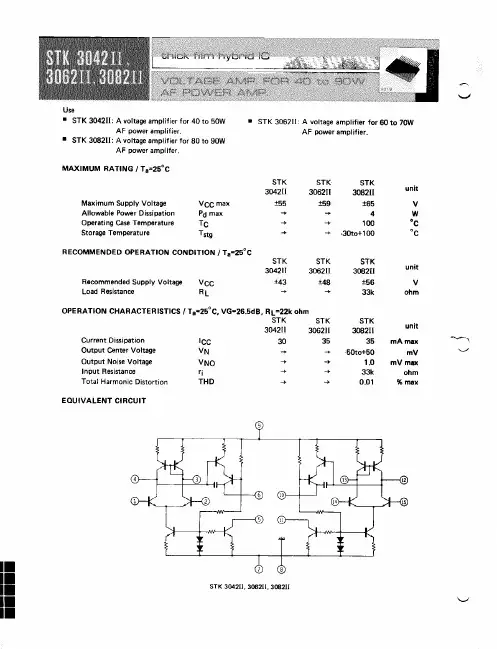

www .be t l u x.co m BL-S30X-14Features:7.62mm (0.3”) Single digit numeric display series Low current operation.Excellent character appearance.Easy mounting on P .C. Boards or sockets. I.C. Compatible.ROHS Compliance.Super BrightElectrical-optical characteristics: (Ta=25) (Test Condition: IF=20mA)Part NoChipVFUnit:V Common CathodeCommon AnodeEmitted ColorMaterialλP (nm)Typ Max Iv TYP.(mcd)BL-S30A-14S-XX BL-S30B-14S-XX Hi Red GaAlAs/GaAs,SH 660 1.852.206BL-S30A-14D-XX BL-S30B-14D-XX Super Red GaAlAs/GaAs,DH 660 1.852.2012 BL-S30A-14UR-XX BL-S30B-14UR-XX Ultra Red GaAlAs/GaAs,DDH6601.852.2014 BL-S30A-14E-XX BL-S30B-14E-XX Orange GaAsP/GaP635 2.102.5010 BL-S30A-14Y-XX BL-S30B-14Y-XX Yellow GaAsP/GaP 585 2.102.5010 BL-S30A-14G-XXBL-S30B-14G-XXGreenGaP/GaP 570 2.202.5010Ultra BrightElectrical-optical characteristics: (Ta=25) (Test Condition: IF=20mA)Part NoChipVFUnit:V Common Cathode Common AnodeEmitted Color MaterialλP(nm)Typ Max Iv TYP .(mcd)BL-S30A-14UHR-XX BL-S30B-14UHR-XXUltra Red AlGaInP645 2.10 2.50 14 BL-S30A-14UE-XXBL-S30B-14UE-XX Ultra Orange AlGaInP 630 2.10 2.50 12 BL-S30A-14YO-XX BL-S30B-14YO-XXUltra Amber AlGaInP 619 2.10 2.50 12 BL-S30A-14UY-XXBL-S30B-14UY-XX Ultra Yellow AlGaInP 590 2.10 2.50 12 BL-S30A-14UG-XX BL-S30B-14UG-XX Ultra Green AlGaInP574 2.20 2.50 18 BL-S30A-14PG-XX BL-S30B-14PG-XXUltra Pure Green InGaN 525 3.80 4.50 22 BL-S30A-14B-XX BL-S30B-14B-XX Ultra Blue InGaN 470 2.70 4.20 25 BL-S30A-14W-XXBL-S30B-14W-XXUltra WhiteInGaN/2.704.2030-XX: Surface / Lens colorNumber1 2 3 4 5 Ref Surface Color White Black Gray Red Green Epoxy Color WaterclearWhite diffusedRed DiffusedGreen DiffusedYellow Diffusedwww .be t l u x.co m BL-S30X-14Absolute maximum ratings (Ta=25)ParameterS D UR E Y G Unit Forward Current I F 25 2525 25 25 30 mA Power Dissipation P d 60 60 60 60 60 65 mW Reverse Voltage V R5 5 5 5 5 5 V Peak Forward Current I PF (Duty 1/10 @1KHZ)150150150 150150150mAOperation Temperature T OPR -40 to +80 Storage Temperature T STG -40 to +85Lead Soldering Temperature T SOLMax.260±5 for 3 sec Max. (1.6mm from the base of the epoxy bulb)Absolute maximum ratings (Ta=25°C) ParameterUHRUE YO UYUGPGUBUWUnitForward Current I F 30 3030 30 30 3030 30 mA Power Dissipation P d 75 65 65 65 75 110 120 120 mW Reverse Voltage V R55555 555V Peak Forward Current I PF (Duty 1/10 @1KHZ)150150150150150150100100mA Operation Temperature T OPR -40 to +80Storage Temperature T STG-40 to +85Lead Soldering TemperatureT SOLMax.260±5 for 3 sec Max. (1.6mm from the base of the epoxy bulb)w w w.be t l ux.co mBL-S30X-14Package configuration & Internal circuit diagram Notes:1. All dimensions are in millimeters (inches)2. Tolerance is 0.25(0.01")unless otherwise noted.3. Specifications are subject to change without notice.wwu x.co m BL-S30X-14Typical electrical-optical characteristics curves:1.00.503504004505005506006507007508008509009501000(A)(B)(C)(D)(2)(3)(8)(4)(1)(6)(5)(9)(10)Wavelength(nm)RELATIVE INTENSITY Vs WAVELENGTH()p (1) - GaAsP/GaAs 655nm/Red (2) - GaP 570nm/Yellow Green (3) - GaAsP/GaP 585nm/Yellow(4) - GaAsp/GaP 635nm/Orange & Hi-Eff Red (5) - GaP 700nm/Bright Red(6) - GaAlAs/GaAs 660nm/Super Red (8) - GaAsP/GaP 610nm/Super Red(9) - GaAlAs 880nm(10) - GaAs/GaAs & GaAlAs/GaAs 940nm (A) - GaN/SiC 430nm/Blue (B) - InGaN/SiC 470nm/Blue(C) - (D) - InGaN/SiC 505nm/Ultra Green InGaAl/SiC 525nm/Ultra Green504030201001.21.62.0 2.4 2.63.016345285040302010020406080100162,4,8,A 353210.50.20.1-30-20-10102030405060701542310987654321110100100010,00010KHz 3KHz1KHz 300KHz 100KHz F-REFRESH RATE100KHz 30KHz10KHz 3KHz 1KHz 300Hz 100Hz 10987654321110100100010,000FORWARD VOLT AGE (Vf)FORWARD CURRENT VS.FORWARD VOLTAGERELATIVE LUMINOUSINTENSITY VS. FORWARD CURRENTAMBIENT TEMPERATURE T a()FORWARD CURRENT VS. AMBIENT TEMPERATUREtp-PULSE DURATION uS (1,2,3,4,6,8,B.D.J.K)NOTE:25 free air temperature unless otherwise specifiedtp-PULSE DURATION uSFORWARD CURRENT(mA)FORWARD CURRENT (mA)RELATIVE LUMINOUS INTENSITYFORWARD CURRENT(mA)RELATIVE LUMINOUS INTENSITYAMBIENT TEMPERATURE T a()(5)Ipeak MAX.IDC MAX.Ipeak MAX.IDC MAX.。
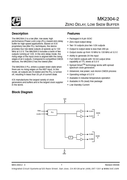
MK2304-2Z ERO D ELAY, L OW S KEW B UFFERDescriptionThe MK2304-2 is a low jitter, low skew, highperformance Phase Lock Loop (PLL) based zero delaybuffer for high speed applications. Based on ICS’proprietary low jitter PLL techniques, the deviceprovides four low skew outputs at speeds up to 133MHz at 3.3 V. The MK2304-2 includes a bank of twooutputs running at 1/2X. In the zero delay mode, therising edge of the input clock is aligned with the risingedges of all 4 outputs. Compared to competitive CMOSdevices, the MK2304-2 has the lowest jitter.The MK2304-2 PLL enters a power-down state whenthere are no rising edges on the REF input. In thismode, all outputs are tri-stated and the PLL is turnedoff, resulting in leass than 25 µA of current draw.ICS manufactures the largest variety of clockgenerators and buffers and is the largest clock supplierin the world.Features•Packaged in 8 pin SOIC•Zero input-output delay•Two 1X outputs plus two 1/2X outputs•Output to output skew is less than 200 ps•Output clocks up from 10 MHz to 133 MHz at 3.3 V•Ability to generate 2X the input•Full CMOS outputs with 18 mA output drivecapability at TTL levels at 3.3 V•Spread Smart TM technology works with spreadspectrum clock generators•Advanced, low power, sub micron CMOS process•Operating voltage of 3.3 V•Available in industial temperature operation•Available in Pb (lead) free package•Low Standby CurrentBlock DiagramZ ERO D ELAY , L OW S KEW B UFFERPin Assignment Feedback Configuration TablePin DescriptionsExternal ComponentsThe Mk2304-2 requires a minimum number of external components for proper operation. Decouplingcapacitors of 0.1µF should be connected between VDD and GND, as close to the part as possible. A 33Ωseries terminating resistor should be used on each clock output to reduce reflections.Feedback FromCLKA1:A2CLKB1:B2Bank A CLKIN CLKIN/2Bank B2XCLKINCLKINPin NumberPin Name Pin Type Pin Description1REF Input Clock input. Connect to input clock source, 5 V tolerant input. 2 CLKA1Output Clock A1 output.3CLKA2Output Clock A2 output.4GND Power Connect to ground.5CLKB1Output Clock B1 output.6CLKB1Output Clock B2 output.7VDD Power 3.3V Power Supply.8FBKInputPLL feedback inputZ ERO D ELAY , L OW S KEW B UFFERAbsolute Maximum RatingsStresses above the ratings listed below can cause permanent damage to the MK2304-2. These ratings, which are standard values for ICS commercially rated parts, are stress ratings only. Functional operation of the device at these or any other conditions above those indicated in the operational sections of thespecifications is not implied. Exposure to absolute maximum rating conditions for extended periods can affect product reliability. Electrical parameters are guaranteed only over the recommended operating temperature range.Recommended Operation ConditionsDC Electrical CharacteristicsVDD=3.3 V ±10%, Amb temp -40° C to 85° CItemRatingSupply Voltage, VDD 7 VAll Inputs and Outputs-0.5 V to VDD+0.5 V Ambient Operating Temperature (commercial)0 to +70 °C Ambient Operating Temperature (industrial)-40 to +85 °C Storage Temperature -65 to +150 °C Junction Temperature 125 °C Soldering Temperature260 °CParameterMin.Typ.Max.UnitsAmbient Operating Temperature (commercial)0+70°C Ambient Operating Temperature (industrial)-40+85°C Power Supply Voltage (measured in respect to GND)+3.0+3.6VParameterSymbolConditions Min.Typ.Max.UnitsOperating Voltage VDD 3.0 3.6V Input High Voltage V IH 2V Input Low Voltage V IL 0.8V Output High Voltage V OH I OH = -8 mA 2.4V Output Low Voltage V OL I OL = 8 mA 0.4V Operating Supply Current 100 MHz, CLKIN IDD No Load 45mAStand by Supply Current 0 MHz, CLKIN IDD No Load 1225uA Short Circuit Current I OS Each output TBD mA Input Capacitance C INFBIN7pF Power-up Time50msZ ERO D ELAY , L OW S KEW B UFFERAC Electrical CharacteristicsVDD = 3.3V ±10%, Ambient Temperature -40° C to 85° CThermal CharacteristicsParameterSymbol ConditionsMin.Typ.Max.UnitsOutput Frequency FBIN to CLKA1, 30 pF Load 10100MHz Output Frequency FBIN to CLKA1,15 pf Load10133MHz Output Rise Time t OR 0.8 to 2.0 V , C L =30 pF 2.2ns Output Rise Time t OR 0.8 to 2.0 V , C L =15 pF 1.5ns Output Fall Time t OF 0.8 to 2.0 V , C L =30 pF 2.2ns Output Fall Time t OF0.8 to 2.0 V , C L =15 pF 1.5ns Output Clock Duty Cycle At 1.4 V , C L =30 pf 405060%Output Clock Duty Cycle At 1.4 V , C L =15 pf 455065%Device-to-Device skew, equally loadedRising edges at VDD/2500ps Output-to-Output skew, equally loaded, On same bank Rising edges at VDD/2200ps Skew from Output Bank A to Output Bank BAll outputs equally loaded400ps Delay CLKIN Rising Edge to FBIN Rising Edge Measured at VDD/2±250ps Cycle-to-Cycle Jitter30 pF loads66.67 MHz outputs 400ps 15 pF loads66.67 MHz outputs375ps PLL Lock Timet LOCKStable power supply, valid clocks on CLKIN, FBIN1msParameterSymbolConditionsMin.Typ.Max.UnitsThermal Resistance Junction to AmbientθJA Still air 120°C/W θJA 1 m/s air flow 115°C/W θJA 3 m/s air flow105°C/W Thermal Resistance Junction to CaseθJC58°C/WZ ERO D ELAY , L OW S KEW B UFFERPackage Outline and Package Dimensions (8-pin SOIC, 150 Mil. Narrow Body)Package dimensions are kept current with JEDEC Publication No. 95Ordering InformationParts that are ordered with a "LF" suffix to the part number are the Pb-Free configuration and are RoHS compliant.While the information presented herein has been checked for both accuracy and reliability, Integrated Circuit Systems (ICS) assumes no responsibility for either its use or for the infringement of any patents or other rights of third parties, which would result from its use. No other circuits, patents, or licenses are implied. This product is intended for use in normal commercialapplications. Any other applications such as those requiring extended temperature range, high reliability, or other extraordinary environmental requirements are not recommended without additional processing by ICS. ICS reserves the right to change any circuitry or specifications without notice. ICS does not authorize or warrant any ICS product for use in life support devices or critical medical instruments.Part / Order NumberMarkingShipping PackagingPackageTemperatureMK2304S-22304S-02Tubes 8-pin SOIC 0 to 70° C MK2304S-2T 2304S-02Tape and Reel8-pin SOIC 0 to 70° C MK2304S-2I 2304S02I Tubes 8-pin SOIC -40° C to 85° C MK2304S-2IT 2304S02I Tape and Reel8-pin SOIC -40° C to 85° C MK2304S-2LF 2304S02L Tubes 8-pin SOIC 0 to 70° C MK2304S-2LFT 2304S02L Tape and Reel8-pin SOIC 0 to 70° C MK2304S-2ILF 2304S2IL Tubes 8-pin SOIC -40° C to 85° C MK2304S-2ILFT2304S2ILTape and Reel8-pin SOIC-40° C to 85° C。
302-321传感器测量原理|温度传感器虽然铂(Pt )电阻具有最低的TC ,他们不仅是最精确的电阻式温度传感器,而且还可以拥有最佳的老化稳定性。
它们是目前市场上指定的“ PT 100 ”或“ PT 1000”( 100 Ω或1,000 Ω在20℃参考温度标称电阻)的各种不同公差等级(最高0.1 ℃)(下图5 )。
在温度高达1000℃左右,厚膜铂传感器适用的铂层已经稳定了特殊的添加剂。
厚膜电阻器(PTC / NTC)的厚膜膏同时具有高电阻(低表面积的要求)及正和负温度系数通常用作温度传感器,用于补偿的目的。
它们具有非线性特性曲线(这虽然是不作为“弯曲”为固体的NTC电阻的曲线),并适用于激光微调。
测量效果是通过从NTC 和PTC材料形成分压器电路的改进。
单晶硅半导体电阻器(PTC)从根本上说,具有单晶半导体材料,例如硅(Si)的温度传感器,它可以进一步包括有源和无源电路元件,所述传感器芯片(在测量点处的初始信号调理)上。
由于所涉及的更小的公差,其生产采用了“扩散电阻”的原则(图6a)。
的电流流过测量电阻和通过到达硅本体材料前的表面点接触。
那么它的收益,分布广泛,以反图。
6 A设计B特性曲线1联系人2钝化(氮化物,氧化物)3 Si衬底4反电极无连接R(T )温度相关电阻器7扩展电阻传感器(单极型温度高达300°C)详细A N + 1 2 3 A 1 NAE0826Y 8塞贝克效应1 T2青新创意T1的一些金属材料的热电电压青新创意mV/100 °C康铜镍-3.40 -1.90 -0.28 PALADIUM白金0.00 +0.75铜锰氧化物0.60铁1.88 2 > NAE0827Y 3热电电压青新创意硅44.80传感器测量原理|温度传感器| 303电极覆盖的传感器芯片的基础。
除了高再现性的材料常数,在接触点(高准确度由于照相平版印刷法生产)背后的高电流密度,主要定义了传感器的电阻。
