欧司朗LED灯珠 G4_V1 1.5W技术资料
- 格式:pdf
- 大小:562.44 KB
- 文档页数:6
电磁光谱可见光仅仅是电磁辐射中的一小部分,其亮度和颜色能够被人眼所感知到。
电磁辐射是能量的一种形式,该辐射的光谱表述了它的能量构成。
电磁辐射的全光谱X围很广,涵盖了能量较高的短波X射线辐射以与能量较低的长波无线电波。
辐射与人的感知我们对光的感知实质上是把光通过棱镜分光的方式分解成各种光谱成分。
我们的大脑为这些光谱中的不同成分分配特定的颜色。
光速是光在真空中的传播速度,近似为每秒300,000千米。
实际上,所有的电磁波都是以这个速度传播的。
地球距离太阳约为1亿5千万千米,光从太阳到达地球大约需要8分钟。
光谱光就是人眼能够感知到的电磁辐射,其波长X围大约在380 nm至780 nm。
眼睛眼睛是一种光学系统,能够在视网膜上产生图像。
它由各种不同的部分组成,包括角膜、水状体、虹膜、晶状体以与玻璃体等,使眼睛能够针对以105系数变化的照明水平简单而快速地做出反应。
眼睛能够感知的最小照度为10-12勒克斯〔相当于夜空中黯淡的星光〕。
眼睛眼睛是一种光学系统,能够在视网膜上产生图像。
它由各种不同的部分组成,包括角膜、水状体、虹膜、晶状体以与玻璃体等,使眼睛能够针对以105系数变化的照明水平简单而快速地做出反应。
眼睛能够感知的最小照度为10-12勒克斯〔相当于夜空中黯淡的星光〕。
光的基础理论辐射度学参数和光度学参数之间存在着差别。
辐射度学参数是纯粹的技术参数,不涉与光对人类的影响作用。
这些参数可从功率单位瓦特推导得到。
而光度学参数则往往需要考虑到人眼的光谱响应曲线〔V<λ>曲线〕。
因此,光度学参数与人类的视觉灵敏度有着特殊的联系。
光度学参数是从光通量单位流明推导得到。
光谱响应曲线是由以下关系产生的:人眼可以看到的辐射位于波长380 nm的蓝光至波长780 nm的红光区域内。
在波长555 nm附近的绿光光谱区域,人眼的灵敏度最高。
而在波长更长或更短的区域内,人眼的灵敏度降低,这就表示在这些波长区域内需要更高的辐射功率才能获得同等的亮度感受。
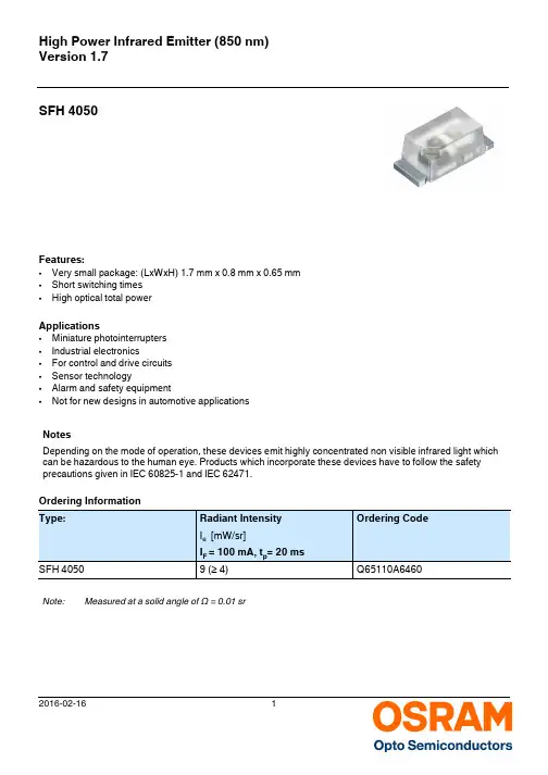
High Power Infrared Emitter (850 nm)Version 1.7SFH 4050Ordering Information Features: •Very small package: (LxWxH) 1.7 mm x 0.8 mm x 0.65 mm •Short switching times •High optical total power Applications•Miniature photointerrupters •Industrial electronics •For control and drive circuits •Sensor technology •Alarm and safety equipment •Not for new designs in automotive applications NotesDepending on the mode of operation, these devices emit highly concentrated non visible infrared light which can be hazardous to the human eye. Products which incorporate these devices have to follow the safety precautions given in IEC 60825-1 and IEC 62471.Note:Measured at a solid angle of Ω = 0.01 srMaximum Ratings (T= 25 °C)Characteristics (TGrouping (T= 25 °C)Note:measured at a solid angle of Ω = 0.01 srOnly one group in one packing unit (variation lower 2:1).Relative Spectral Emission 3) page 12 I rel = f(λ), T A = 25°CRadiant Intensity 3) page 12I e / I e (100 mA) = f(I F ), single pulse, t p = 25 µs, T A = 25°C7000nm %OHF0413220406080100950750800850I λOHL0171510-3mA 101105510-1-2510e I I F1011021031055Max. Permissible Forward Current I F = f (T A ), RthJA = 450 K/WForward Current 3) page 12I F = f(V F ), single pulse, t p = 100 µs, T A = 25°CPermissible Pulse Handling CapabilityI F = f(t p ), T A = 25 °C, duty cycle D = parameterPermissible Pulse Handling CapabilityI F = f(t p ), T A = 85 °C, duty cycle D = parameterOHR0088302040608010012020406080100120mA˚C AR thjA = 450 K/WOHL01713I 10-40.51 1.52 2.5V3100A0F-1105510-2-3510t pA I10101010101010s 2100.10.20.30.40.50.60.70.80.91.1t p0A I 10101010101010s 2100.10.20.30.40.50.60.70.81.0Radiation Characteristics 3) page 12 I rel = f(ϕ), T A = 25°CPackage OutlineDimensions in mm (inch).PackageSmartLED (EIA 0603), Epoxy, colourless, slightly diffused100˚90˚80˚70˚60˚50˚GPLY7036+0.05 (0.002)0.125 (0.005)-0.05 (0.002)0.65 (0.026)±0.1 (0.004)±0.05 (0.002)Approximate Weight:2.1 mgRecommended Solder PadDimensions in mm (inch).OHAPY606Alternative Solder PadDimensions in mm (inch).Reflow Soldering ProfileProduct complies to MSL Level 2 acc. to JEDEC J-STD-020D.01OHPY3832Copper solder pad50100150200250300t ˚CTapingDimensions in mm [inch].* slope calculation D T/D t: D t max. 5 s; fulfillment for the whole T-rangeTape dimensions [mm]Reel dimensions [mm]Barcode-Product-Label (BPL)Tape and Reel8 mm tape with 5000 pcs. on ∅ 180 mm reelOHA04563(G) GROUP:1234567890(1T) LOT NO:(X) PROD NO:123456789LX XXXXRoHS CompliantBIN1: XX-XX-X-XXX-XML X Temp STXXX °C XPack: RXX DEMYX_X123_1234.1234 X9999(Q)QTY: 4 X _1234.1234 X XX-X-X3_1234X-XX-X- RXX XXXX_X123_123XX-XX-X 234Pack: RX D) D/C:/C:(9D) D 567890NO:123456789torsH NO:123456uctors OptoE XAM PL E678901234(9D) D/C:(6P) BATCH NO:1234567890OSRAM Opto XX-XX-X-X SemiconductorsDry Packing Process and MaterialsNote:Moisture-sensitive product is packed in a dry bag containing desiccant and a humidity card.Regarding dry pack you will find further information in the internet. Here you will also find the normative references like JEDEC.Transportation Packing and MaterialsDimensions of transportation box in mmOHA00539Barcode labelDisclaimerLanguage english will prevail in case of any discrepancies or deviations between the two language wordings. Attention please!The information describes the type of component and shall not be considered as assured characteristics.Terms of delivery and rights to change design reserved. Due to technical requirements components may contain dangerous substances.For information on the types in question please contact our Sales Organization.If printed or downloaded, please find the latest version in the Internet.PackingPlease use the recycling operators known to you. We can also help you – get in touch with your nearest sales office. By agreement we will take packing material back, if it is sorted. You must bear the costs of transport. For packing material that is returned to us unsorted or which we are not obliged to accept, we shall have to invoice you for any costs incurred.Components used in life-support devices or systems must be expressly authorized for such purpose! Critical components* may only be used in life-support devices** or systems with the express written approval of OSRAM OS.*) A critical component is a component used in a life-support device or system whose failure can reasonably be expected to cause the failure of that life-support device or system, or to affect its safety or the effectiveness of that device or system.**) Life support devices or systems are intended (a) to be implanted in the human body, or (b) to support and/or maintain and sustain human life. If they fail, it is reasonable to assume that the health and the life of the user may be endangered.Glossary1)Thermal resistance: junction -ambient, mounted on PC-board (FR4), padsize 5 mm2 each2)Thermal resistance: junction - soldering point, of the device only, mounted on an ideal heatsink (e.g. metal block)3)Typical Values: Due to the special conditions of the manufacturing processes of LED, the typical data or calculated correlations of technical parameters can only reflect statistical figures. These do not necessarily correspond to the actual parameters of each single product, which could differ from the typical data and calculated correlations or the typical characteristic line. If requested, e.g. because of technical improvements, these typ. data will be changed without any further notice.Published by OSRAM Opto Semiconductors GmbHLeibnizstraße 4, D-93055 Regensburg © All Rights Reserved.。
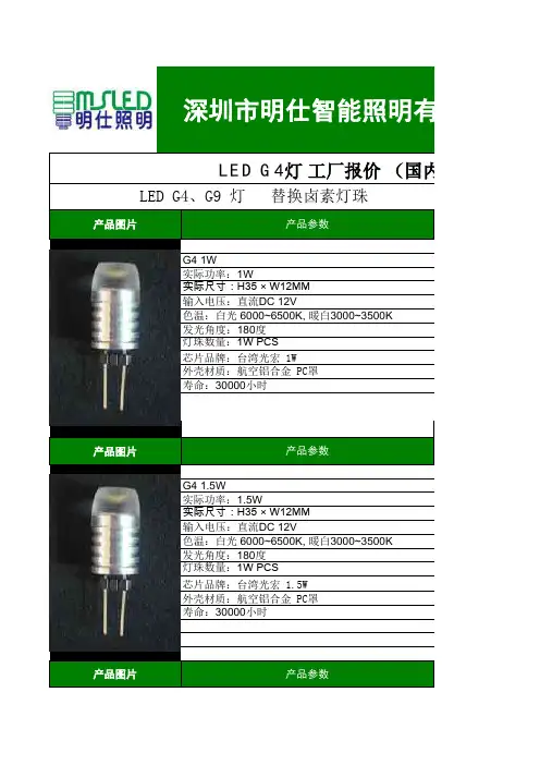
深圳市明仕智能照明有限LED G4灯工厂报价(国内) LED G4、G9 灯 替换卤素灯珠产品图片产品参数G4 1W实际功率:1W实际尺寸:H35 × W12MM输入电压:直流DC 12V色温:白光 6000~6500K, 暖白3000~3500K发光角度:180度灯珠数量:1W PCS芯片品牌:台湾光宏 1W外壳材质:航空铝合金 PC罩寿命:30000小时产品图片产品参数G4 1.5W实际功率:1.5W实际尺寸:H35 × W12MM输入电压:直流DC 12V色温:白光 6000~6500K, 暖白3000~3500K发光角度:180度灯珠数量:1W PCS芯片品牌:台湾光宏 1.5W外壳材质:航空铝合金 PC罩寿命:30000小时产品图片产品参数G4 3W实际功率:3W实际尺寸:H42 × W18MM输入电压:直流DC 12V色温:白光 6000~6500K, 暖白3000~3500K发光角度:180度灯珠数量:1W PCS芯片品牌:台湾光宏 3W外壳材质:航空铝合金 PC罩寿命:30000小时产品图片产品参数G4 3W实际功率:3W实际尺寸:H42 × W18MM输入电压:交流AC/直流DC 12V 通用色温:白光 6000~6500K, 暖白3000~3500K发光角度:180度灯珠数量:3W PCS芯片品牌:台湾光宏 3W外壳材质:航空铝合金 PC罩寿命:30000小时产品图片产品参数G4 4W实际功率:4W实际尺寸:H42 × W18MM输入电压:交流AC/直流DC 12V 通用色温:白光 6000~6500K, 暖白3000~3500K发光角度:180度灯珠数量:3W PCS芯片品牌:台湾光宏 4W外壳材质:航空铝合金 PC罩寿命:30000小时产品图片产品参数G4 4W实际功率:4W实际尺寸:H38 × W18MM输入电压:交流AC/直流DC 12V 通用色温:白光 6000~6500K, 暖白3000~3500K发光角度:330度灯珠数量:0.22W 18PCS芯片品牌:晶元外壳材质:三芯片 SMD 5050寿命:30000小时产品图片产品参数G4 6W实际功率:6W实际尺寸:H38 × W19MM输入电压:交流AC/直流DC 12V 通用色温:白光 6000~6500K, 暖白3000~3500K发光角度:330度灯珠数量:0.22W 34PCS芯片品牌:晶元外壳材质:三芯片 SMD 5050寿命:30000小时产品图片产品参数G4 4W实际功率:4W实际尺寸:H46 × W18MM输入电压:直流DC 12V色温:白光 6000~6500K, 暖白3000~3500K发光角度:330度灯珠数量:0.22W 18PCS芯片品牌:台湾奇力外壳材质:三芯片 SMD 5050寿命:30000小时产品图片产品参数G4 5W实际功率:4.5W实际尺寸:H46 × W18MM输入电压:直流DC 12V色温:白光 6000~6500K, 暖白3000~3500K发光角度:330度灯珠数量:1.5W 3PCS芯片品牌:台湾奇力外壳材质:航空铝合金 PC罩寿命:30000小时产品图片产品参数G4 6W实际功率:6W实际尺寸:H46 × W18MM输入电压:直流DC 12V色温:白光 6000~6500K, 暖白3000~3500K发光角度:330度灯珠数量:1.5W 4PCS芯片品牌:台湾奇力外壳材质:航空铝合金 PC罩寿命:30000小时产品图片产品参数G9 3W实际功率:3W实际尺寸:H65 × W22MM输入电压:220V色温:白光 6000~6500K, 暖白3000~3500K发光角度:330度灯珠数量:0.22W 11PCS芯片品牌:台湾奇力 三芯片 SMD 5050外壳材质:外航空铝合金 + 内陶瓷寿命:30000小时注明:1、以上报价是批量100只以上的价格,不含税。
LED灯技术参数LED灯是一种使用固态发光二极管(LED)作为光源的照明装置。
相比于传统的白炽灯和荧光灯,LED灯具有更高的能效、更长的寿命和更好的色彩表现,因此在各个领域得到广泛应用。
在选择和购买LED灯时,了解其技术参数是非常重要的,下面就介绍LED灯的一些常见技术参数。
1. 亮度:亮度是LED灯一个重要的技术参数,它通常以流明(lm)为单位来衡量。
流明数表示单位时间内灯光发出的总光功率。
亮度直接关系到LED灯的照明效果,一般情况下,亮度越高代表LED灯越亮。
2.色温:色温是指光源发出的光线的色彩特性,通常以开尔文温标(K)来衡量。
低色温的光源会呈现出暖黄色的光,而高色温的光源则呈现出冷蓝色或自然白色的光。
不同的场景和需求可能需要不同色温的光源,所以选择合适的色温对于LED灯的应用非常重要。
3.发光角度:发光角度是指LED灯光的辐射范围,也称为光束角或辐射角。
通常以度(°)为单位来表示。
发光角度越小,光线的聚焦效果就越好,适用于需要有针对性照明的场合;而发光角度越大,光线的分布就越均匀,适用于需要较大范围照明的场合。
4.色彩指数(CRI):色彩指数是LED灯所发出光线的还原能力的度量。
一般来说,CRI的范围是0-100,越高代表LED灯能更好地还原物体原本的颜色。
对于一些对色彩还原要求较高的场合,如艺术展览和美术馆,选择CRI较高的LED灯是很重要的。
5.耗电量:耗电量是指LED灯使用的电能,通常以瓦特(W)为单位。
相比传统的白炽灯和荧光灯,LED灯的耗电量更低,能够提供更高的能效。
6.寿命:寿命是指LED灯的使用寿命,通常以小时(h)为单位。
LED 灯的寿命一般在10,000小时以上,远远超过传统的白炽灯和荧光灯。
这意味着可以减少更换灯泡的频率和维护成本。
7.显色指数(Ra):显色指数是对白光光源所发出光线中各种颜色的还原度量。
与色彩指数类似,Ra的范围也是0-100,越高代表LED灯的还原能力越好。
LED G4灯珠
目前,国内光源产品的发光类别有三种,分别是白炽灯通过钨丝发光,通过热能转化为光,但比较耗能且耐高温不足的情况下使用寿命也极为短。
还有就是荧光灯,通过荧光粉发光。
荧光灯启动响应时间较长,且电子辐射较大及污染严重。
最后就是LED,由半导体材料制成,通过电能激发转化为光能,有节能,环保,无辐射等多种优点。
国内常规的光源接头规格分别有:E14 E27 B22 G4 G9 G10 G5.3等等。
其中E14 E27 B22被广泛用于民居。
G10 G5.3 G9更多是用于商照。
而G4则可以两者通用。
G4规格的意思是:使用两个或者两个以上的插脚灯头,插脚的中心点距离为4mm。
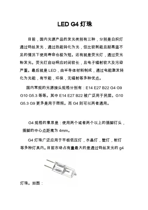
G4灯珠广泛应用于平板低压灯,水晶灯,壁灯,射灯等多种灯具内。
目前市场占有量最大的是通过钨丝发光的g4
灯珠。
如图:
该产品别称分别有:g4灯泡g4插泡g4灯珠卤素灯珠等等。
这款钨丝发光的灯珠功耗较高,且使用寿命短。
正常功率有20w 40w 60w 使用寿命在300小时左右。
而本文标题中的所说的ledg4灯珠,是目前新近研发的产品。
有节能使用寿命长的优点。
是目前替代老款钨丝发光的理想产品。
具体如图所示
该款产品的优点在于只有1-3w,使用寿命在30000小时左右。
且有白光和暖白可供选择。
整体是采用led贴片光源热度低发光性能好,使用高级硅胶合成材料封装。
透光率及散热性比较好。
且降低运输破损风险。
High Power Infrared Emitter (940 nm)Version 1.4/ OS-IN-2015-033SFH 4248Ordering Information Features: •High Power Infrared LED •Short switching times •Half angle: ± 15°•High forward current allowed at high temperature •The product qualification test plan is based on the guidelines of AEC-Q101-REV-C, Stress Test Qualification for Automotive Grade Discrete Semiconductors.Applications •Infrared Illumination for cameras •IR data transmission •Sensor technology NotesDepending on the mode of operation, these devices emit highly concentrated non visible infrared light which can be hazardous to the human eye. Products which incorporate these devices have to follow the safety precautions given in IEC 60825-1 and IEC 62471.Note:Measured at a solid angle of Ω = 0.01 srMaximum Ratings (T= 25 °C)Characteristics (TGrouping (T= 25 °C)Note:measured at a solid angle of Ω = 0.01 srOnly one group in one packing unit (variation lower 2:1).Relative Spectral Emission 3) page 12 I rel = f(λ), T A = 25°CRadiant Intensity 3) page 12I e / I e (100 mA) = f(I F ), single pulse, t p = 25 µs, T A = 25°C8000nm %OHF0413420406080100I λ8509009501025OHF0382110-3mA 101105510-1-2510e e I I F1011021031055(100 mA)Max. Permissible Forward Current I F, max = f(T A ), R thJA = 300 K / WForward Current 3) page 12I F = f(V F ), single pulse, t p = 100 µs, T A = 25°CPermissible Pulse Handling CapabilityI F = f(t p ), T A = 25 °C, duty cycle D = parameterPermissible Pulse Handling CapabilityI F = f(t p ), T A = 85 °C, duty cycle D = parameter00˚C T I mAOHL01716A2040608010012020406080120OHF03822I 10-4V 100A0F-1105510-2-35100.51 1.52 2.521010101010t p1010s 100A I 0.20.40.60.81.01.2t pA I 10101010101010s 2100.10.20.30.40.50.60.70.80.91.1Radiation Characteristics 3) page 12 I rel = f(ϕ)Package OutlineDimensions in mm (inch).OHL0002150˚60˚70˚80˚90˚100˚GPLY6127PinningPackagePower TOPLED with Lens Approximate Weight:37 mgRecommended Solder PadDimensions in mm.Reflow Soldering ProfileProduct complies to MSL Level 2 acc. to JEDEC J-STD-020D.01050100150200250300tT ˚CAll temperatures refer to the center of the package, measured on the top of the component * slope calculation D T/D t: D t max. 5 s; fulfillment for the whole T-rangeTapingDimensions in mm. Tape and Reel12 mm tape with 2000 pcs. on ∅ 180 mm reelTape dimensions [mm]Reel dimensions [mm]Barcode-Product-Label (BPL)Dry Packing Process and MaterialsNote:Moisture-sensitive product is packed in a dry bag containing desiccant and a humidity card.Regarding dry pack you will find further information in the internet. Here you will also find the normative references like JEDEC.OHA04563(G) GROUP:1234567890(1T) LOT NO:(X) PROD NO:123456789LX XXXXRoHS CompliantBIN1: XX-XX-X-XXX-XML X Temp STXXX °C XPack: RXX DEMYX_X123_1234.1234 X 9999(Q)QTY: 4 X_1234.1234 X XX-X-X3_1234X-XX-X- RXX XXXX_X123_123XX-XX-X 234Pack: RX D) D/C:/C:(9D) D 567890NO:123456789torsH NO:123456uctors OptoE XAM PL E678901234(9D) D/C:(6P) BATCH NO:1234567890OSRAM Opto XX-XX-X-X Semiconductors OHA00539Barcode labelTransportation Packing and MaterialsDimensions of transportation box in mmDisclaimerLanguage english will prevail in case of any discrepancies or deviations between the two language wordings. Attention please!The information describes the type of component and shall not be considered as assured characteristics.Terms of delivery and rights to change design reserved. Due to technical requirements components may contain dangerous substances.For information on the types in question please contact our Sales Organization.If printed or downloaded, please find the latest version in the Internet.PackingPlease use the recycling operators known to you. We can also help you – get in touch with your nearest sales office. By agreement we will take packing material back, if it is sorted. You must bear the costs of transport. For packing material that is returned to us unsorted or which we are not obliged to accept, we shall have to invoice you for any costs incurred.Components used in life-support devices or systems must be expressly authorized for such purpose! Critical components* may only be used in life-support devices** or systems with the express written approval of OSRAM OS.*) A critical component is a component used in a life-support device or system whose failure can reasonably be expected to cause the failure of that life-support device or system, or to affect its safety or the effectiveness of that device or system.**) Life support devices or systems are intended (a) to be implanted in the human body, or (b) to support and/or maintain and sustain human life. If they fail, it is reasonable to assume that the health and the life of the user may be endangered.Glossary1)Thermal resistance: junction -ambient, mounted on PC-board (FR4), padsize 16 mm2 each2)Thermal resistance: junction - soldering point, of the device only, mounted on an ideal heatsink (e.g. metal block)3)Typical Values: Due to the special conditions of the manufacturing processes of LED, the typical data or calculated correlations of technical parameters can only reflect statistical figures. These do not necessarily correspond to the actual parameters of each single product, which could differ from the typical data and calculated correlations or the typical characteristic line. If requested, e.g. because of technical improvements, these typ. data will be changed without any further notice.Published by OSRAM Opto Semiconductors GmbHLeibnizstraße 4, D-93055 Regensburg © All Rights Reserved.。
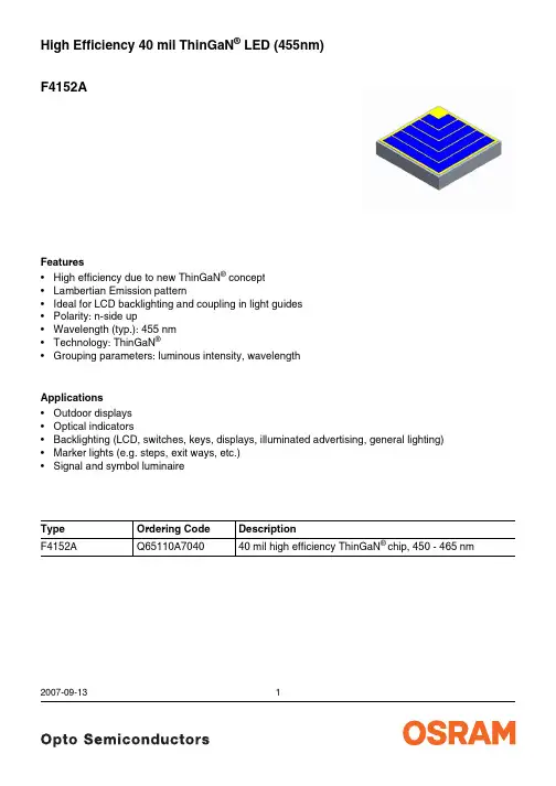
F4152AHigh Efficiency 40 mil ThinGaN ®LED (455nm)2007-09-131Features •High efficiency due to new ThinGaN ® concept •Lambertian Emission pattern•Ideal for LCD backlighting and coupling in light guides •Polarity: n-side up•Wavelength (typ.): 455 nm •Technology: ThinGaN ®•Grouping parameters: luminous intensity, wavelengthApplications •Outdoor displays •Optical indicators•Backlighting (LCD, switches, keys, displays, illuminated advertising, general lighting)•Marker lights (e.g. steps, exit ways, etc.)•Signal and symbol luminaireType Ordering Code DescriptionF4152AQ65110A704040 mil high efficiency ThinGaN ® chip, 450 - 465 nmElectrical values1)(T A = 25 °C)Parameter Symbol Value2)Unitmin.typ.max. Dominant wavelengthI F = 350 mA, pulsedλdom450465nm Reverse voltageI R = 10µAV R10VForward voltageI F = 350 mA, pulsed VF2.73.8VRadiant PowerI F = 350 mA, pulsedΙV32 a.u.1)Measurement limits describe actual settings and do not include measurement uncertainties. Each wafer and fragmentof a wafer is subject to final testing. The wafer or its pieces are individually attached on foils (rings). All el. values are referenced to the vendor's measurement system (correlation to customer product(s) is required). Measurement uncertainty +/-15% for brightness, +/- 1nm for wavelength and +/- 0.1V for voltage.2)Due to the special conditions of the manufacturing processes of LED, the typical data or calculated correlations oftechnical parameters can only reflect statistical figures. These do not necessarily correspond to the actual parameters of each single product, which could differ from the typical data and calculated correlations or the typical characteristic line. If requested, e.g. because of technical improvements, these typ. data will be changed without any further notice.2007-09-1322007-09-133Binning Maximum Ratings 1)Radiant Power 450 - 455 nm455 - 460 nm460 - 465 nm28.0 - 35.2 a.u.A1B1C135.2 - 41.2 a.u.A2B2C241.2 - 48.4 a.u.A3B3C348.4 - 56.8 a.u.A4B4C4> 56.8 a.u.A5B5C5ParameterSymbol Value Unit Maximum Operating temperature range T op -40...+100°C Maximum forward current (T A = 25°C)I F 700mA Minimum forward current (T A = 25°C)I F100mA Maximum surge Current (T A = 25°C)t p = 10 µs, D = 0.05I peak0.7A Maximum junction temperatureT j125°C1)Maximum ratings are strongly package dependent and may differ between different packages. The values given represent the chip in an OSRAM Opto Semiconductor’s Platinum Dragon® package.Mechanical values1)Parameter Symbol Value2)Unitmin.typ.max.Length of chip edge (x-direction)L x0.95 1.00 1.05mm Length of chip edge (y-direction)L y0.95 1.00 1.05mm Diameter of the wafer D50.8mmDie height H170190210µm Diameter of bondpad d130150170µm Additional informationMetallization frontside Gold partialMetallization backside AuDie bonding Epoxy bonding1)All chips are checked according to the following procedure and the OSRAM OS specification of the visual inspectionA63501-Q0013-N001-*-76G3:Unless otherwise described below, the quality level of the final visual inspection shall comply to an AQL 0,4 (according MIL-STD-105D, level II), if the customer performes an incoming visual inspection of a shipment. The quality inspection (final visual inspection) is performed by production. An additional visual inspection step as special release procedure by QM after the final visual inspection is not installed.2)Due to the special conditions of the manufacturing processes of LED, the typical data or calculated correlations oftechnical parameters can only reflect statistical figures. These do not necessarily correspond to the actual parameters of each single product, which could differ from the typical data and calculated correlations or the typical characteristic line. If requested, e.g. because of technical improvements, these typ. data will be changed without any further notice2007-09-1342007-09-135Chip OutlinesDimensions are specified as typicalvalues as follows: mm (inch).Published by OSRAM Opto Semiconductors GmbH Wernerwerkstrasse 2, D-93049 Regensburg © All Rights Reserved.Attention please!The information generally describes the type of component and shall not be considered as assured characteristics or detailed specification.Terms of delivery and rights to change design reserved. Due to technical requirements components may contain dangerous substances. For information on the types in question please contact our sales organization.Handling and Storage Conditions:Storage time for wafers in sealed condition shall not exceed 6 months (storage ambient conditions: Ta=15...30°C;relative humidity: < 60%).The hermetically sealed shipment lot shall be opened under temperature and moisture controlled cleanroom environment only. Customer has to follow the according rules for disposition of material that can be hazardous for humans and environment. Dice have to be handled ESD sensitive.PackingChips are placed on a blue foil with minimum size of 18 x 18 cm².For shipment the wafers of a shipment lot are arranged to stacks. The stack is put in a plastic ESD bag with a maximum of 14 wafers in one bag. A maximum of 4 bags is put in a packaging box. A maximum of 5 packaging boxes is put in a shipping carton which is sealed for storage and shipment.Please use the recycling operators known to you. We can also help you – get in touch with your nearest sales office. By agreement we will take packing material back, if it is sorted. You will have to bear the costs of transport. For packing material that is returned to us unsorted or which we are not obliged to accept, we shall have to invoice you for any costs incurred.Label and shipping documentsEach wafer is identified with a sticker, which is attached to each wafer. The label shows chip type, wafer number, quantity, binning and the minimum, average and maximum values of voltage, luminous intensity and wavelength. Each wafer shipment includes an additional document, which summarizes the content.Design objectives a) workabilityThe chip design was developed and released based on the the vendor’s standard assembly procedures and packaging. Bond strength properties are in accordance to MIL_STD-750D, method 2037. Whether the chip fits to the customer’s product(c) with its according die and wire bond procedures and packaging must be evaluated by the customer himself. If workability problems arise after this release a mutually conducted problem solving procedure has to be set up, if thechips are suspected of contributing to the problemsb) chip characteristicsThe chips are produced by the vendor with best effort, but on chip level a subset of the chip characteristics can be determined only. Performance of the chip in the customer’s product(s) can only be determined by the customer himself. Returns/ComplaintsTo return material because of technical or logistical reasons a RMA-number is necessary. Samples for analysis purposes can be send to OSRAM OS without credit.Shipping Conditions:If not otherwise arranged, the “General Conditions for the supply of products and services of the electrical and electronics industry” apply for any shipment. If these documents are not familiar to you, please request them at our nearest sales office.Components used in life-support devices or systems must be expressly authorized by us for such purpose! Critical components2), may only be used in life-support devices or systems3) with the express written approval of OSRAM OS.1) Typical (refered to as typ.) data are defined as long-term production mean values and are only given for information. This is not a specified value.2)A critical component is a component used in a life-support device or system whose failure can reasonably be expected to cause the failure of that life-support device or system, or to affect its safety or effectiveness of that device or system.3)Life support devices or systems are intended (a) to be implanted in the human body, or (b) to support and/or maintain and sustain human life. If they fail, it is reasonable to assume that the health of the user may be endangered.2007-09-136。
LED灯珠参数介绍LED(Light Emitting Diode)是一种半导体器件,能够将电能直接转化为光能。
LED灯珠是LED照明产品的核心组成部分,其参数决定了LED灯珠的性能和应用范围。
下面将介绍LED灯珠的常见参数。
1.亮度:LED灯珠的亮度是衡量其辐射光强度的指标,单位为流明(lm)。
亮度决定了LED灯珠的照明效果,一般来说,亮度越高,LED灯的照明效果越好。
2.发光效率:发光效率是指LED灯珠所辐射出来的光能与输入的电能之间的转换效率,一般以光通量(lm/W)来衡量。
发光效率高的LED灯珠能够在相同输入电能的情况下达到更高的亮度。
3.色温:色温是指LED灯珠发出的光的颜色,一般用单位为开尔文(K)的绝对温度来表示。
常见的LED灯珠有暖白光(2700K-3500K)、自然白光(4000K-4500K)、冷白光(5000K-6500K)等不同色温,应用于不同场景和需求。
4.色彩指数:色彩指数是描述光源对物体颜色还原能力的一个指标,用Ra来表示。
Ra越高,光源对物体颜色还原的能力越好,颜色更真实。
常见的LED灯珠色彩指数一般在80以上,达到或接近自然光的还原效果。
5.功率:功率是LED灯珠工作时的电能消耗,单位为瓦特(W)。
功率的大小直接影响到LED灯珠的亮度和发光效率,通常情况下,功率越大,亮度越高。
6.工作电流:工作电流是指LED灯珠正常工作时所需要的电流,单位为安培(A)。
工作电流的大小会影响到LED灯珠的亮度和寿命,过高或过低的电流都会影响到其正常工作。
7.寿命:寿命是指LED灯珠在正常工作状态下可以工作的时间。
LED 灯珠寿命的衡量标准是指其亮度降低到初始值的70%所需要的时间,一般来说,寿命较长的LED灯珠能够在相同亮度下使用更久。
8.耐压:耐压是指LED灯珠能够承受的最大电压。
耐压的大小直接影响LED灯珠在实际应用中的可靠性和稳定性。
9.光束角:光束角是指LED灯珠发出的光的辐射范围。
欧司朗卤素灯规格书1. 产品概述欧司朗卤素灯是一种高效、可靠的照明设备,采用卤素化合物作为填充物,能够提供明亮、稳定的光线。
本规格书将详细介绍欧司朗卤素灯的规格、特性以及适用场景等信息。
2. 产品规格2.1 电气参数•输入电压:220V•频率:50Hz•功率:100W•亮度:5000lm2.2 光学参数•光源类型:卤素灯•色温:3000K•发光角度:120°•显色指数:802.3 外观参数•外壳材质:铝合金•外壳颜色:银白•尺寸:直径 100mm,高度 120mm•重量:500g3. 产品特性3.1 高效节能欧司朗卤素灯采用先进的卤素化合物技术,能够在相同功率下提供更高的亮度。
相比传统的白炽灯,欧司朗卤素灯能够节省能源达到50%,同时提供更明亮的照明效果。
3.2 长寿命欧司朗卤素灯具有较长的使用寿命,平均可达到2000小时以上。
其寿命远远超过传统白炽灯,减少了更换灯泡的频率和维护成本。
3.3 良好的色彩再现性欧司朗卤素灯具有较高的显色指数(80),能够更真实地还原物体的颜色。
无论是家庭照明还是商业照明,欧司朗卤素灯都能提供优质的照明效果,使物体的颜色更加鲜艳、真实。
3.4 环保可靠欧司朗卤素灯不含有汞等有害物质,对环境友好。
同时,其外壳采用高质量的铝合金材料,具有良好的散热性能,保证灯泡的稳定工作,减少故障率。
3.5 安装简便欧司朗卤素灯采用标准的螺口接口设计,容易安装和更换。
用户只需将灯泡插入灯座并旋转即可完成安装,无需使用其他工具。
4. 适用场景欧司朗卤素灯适用于各种室内照明场景,包括家庭、商业、办公等。
其高亮度、高显色指数以及良好的色彩再现性,使其成为展示产品、照明艺术品、商业场所等的理想选择。
5. 注意事项•在安装和更换灯泡时,务必断开电源,避免触电事故发生。
•请勿将灯泡暴露在高温或潮湿的环境中,以免影响其使用寿命。
•请勿用力碰撞或摔落灯泡,以免损坏外壳和内部结构。
6. 售后服务欧司朗公司提供全面的售后服务,包括产品质保、维修和更换等。
LED G4灯最新参数表 LED G4、G9 灯 替换卤素灯珠产品图片MS-TD3-G4 1.5W 2W 3W 4W实测功率:1.2W、1.5W、 2.1W、 2.4W实际尺寸:H55 × W18MM输入电压:AC/DC12V色温:白光 6000~6500K, 暖白3000~3500K光效:1W/80LM发光角度:广角灯珠数量:1-4PCS (3030) SMD芯片品牌:台湾奇力 1PCS 1W外壳材质:导热陶瓷寿命:30000小时产品图片MS-TD3-G9 1.5W 2W 3W 4W实测功率:1.2W、1.5W、 2.1W、 2.4W实际尺寸:H55 × W18MM输入电压:AC/DC12V色温:白光 6000~6500K, 暖白3000~3500K光效:1W/80LM发光角度:广角灯珠数量:1-4PCS (3030) SMD芯片品牌:台湾奇力 1PCS 1W外壳材质:导热陶瓷寿命:30000小时产品图片产品参数MS-G9-3D-2W 3W实测功率:1.8W 2.4W实际尺寸:H65 × W22MM输入电压:200-240V色温:白光 6000~6500K, 暖白3000~3500K光效:2W(180LM)3W(280LM)发光角度:360度灯珠数量:0.22W 11PCS芯片品牌:台湾晶元 芯片 SMD 5050外壳材质:外航空铝合金 + 内陶瓷寿命:30000小时产品图片MS-1D-G4-3 1W 2W 3W 4W实测功率: 2W、 2.4W实际尺寸:H42 × W18MM输入电压:AC/DC12V色温:白光 6000~6500K, 暖白3000~3500K光效:1W/80LM发光角度:150度灯珠数量:1-4PCS芯片品牌:台湾奇力 3030 SMD外壳材质:高导热铝寿命:30000小时产品图片MS-5D-G4 4W 5W实测功率:4W(2.5W) 5W(2.8W)实际尺寸:H42 × W15MM输入电压:AC/DC12V色温:白光 6000~6500K, 暖白3000~3500K光效:4W(280LM)5W(300LM)发光角度:广角灯珠数量:10PCSX0.5W芯片品牌:台湾奇力 3020贴片外壳材质:高导热铝寿命:30000小时产品图片MS-G4-3D-2.5W实际功率:2W实际尺寸:H42 × W10MM输入电压:AC/DC12V色温:白光 6000~6500K, 暖白3000~3500K光效:2.5W(230LM)发光角度:广角灯珠数量:6PCSX0.5W芯片品牌:台湾奇力 3020贴片外壳材质:高导热铝寿命:30000小时产品图片G9-1D-2W 3W实际功率:3W(2.5W)2W(2W)实际尺寸:H60 × W20MM输入电压:AC/DC-220V色温:白光 6000~6500K, 暖白3000~3500K光效:2W(150LM)3W(200LM)发光角度:120度灯珠数量:1PCSX(3W)(2W)芯片品牌:台湾奇力 COB T10外壳材质:高导热铝寿命:30000小时产品图片G4-C5D-5W实测功率:3W实际尺寸:H42 × W17MM输入电压:AC/DC12V色温:白光 6000~6500K, 暖白3000~3500K光效:5W(330LM)发光角度:广角灯珠数量:5PCSX(1W)芯片品牌:台湾奇力 COB 8.5外壳材质:高导热铝寿命:30000小时产品图片G4-1D-1W 1.5W实测功率:1W 1.5W实际尺寸:H42 × W17MM输入电压:AC/DC12V色温:白光 6000~6500K, 暖白3000~3500K发光角度:120度光效:1W(80LM)1.5W(110LM)灯珠数量:1PCSX(1W)(1.5W)芯片品牌:台湾奇力 COB 8.5外壳材质:高导热铝寿命:30000小时产品图片G4-TP3-4W 6W实测功率:2.7W 3.4W实际尺寸:H35 × W18MM输入电压:AC/DC12V色温:白光 6000~6500K, 暖白3000~3500K光效:4W(280LM)6W(380LM)发光角度:360度灯珠数量:18PCSX(0.2W) 27 PCS(0.2W)芯片品牌:台湾奇力 SMD 5050外壳材质:高导热铝寿命:30000小时产品图片G4-TP3-4W 6W实测功率:2.7W 3.4W实际尺寸:H35 × W18MM输入电压:DC12V色温:白光 6000~6500K, 暖白3000~3500K光效:6W(380LM)发光角度:360度灯珠数量:4PCSX(1.5W)芯片品牌:台湾奇力 COB 9X21 T12外壳材质:高导热铝寿命:30000小时参数表。
照明(zhàomíng)常识---外贸人员(rényuán)必备LED灯珠的分类(fēn lèi)按照功率:可分为小功率灯珠(0.5W以下(yǐxià))、中功率灯珠(0.5W)、大功率灯珠(0.5W以上)。
按照封装方式(fāngshì):可分为草帽灯珠、贴片灯珠、COB灯珠按照发光颜色:可以分为白光、红光、蓝光、绿光等等。
特点1、安全性高:LED灯珠的工作电压一般是3.0-3.5V之间,所以安全性高,即使触电,也没有危险。
2、运用灵活:由于体积很小,所以可以灵活运用,做成各种体积、各种类型的灯。
3、超长寿命:理论上LED的寿命是10万个小时,而白炽灯只有1000个小时,节能荧光灯是8000个小时。
4、低碳环保:不含有害物质,如汞等重金属,所以非常环保,光效高决定了它的低碳节能。
光源中没有水银,光束中不含紫外线。
LED是固体发光光源,绿色环保5、高光效性:白炽灯的光效大概15 lm/W,节能荧光灯为50-60 lm/W, LED为100-120 lm/W(科锐实验室为276 lm/W,2013年2月数据)。
6、光线品质高:光线中无紫外线,对人体健康无害。
T5荧光灯管的周长5厘米,T8的8厘米按灯头规格划分为G5灯头(T5)、G13灯头(T8/T10);按PC罩类型A:扩散罩(乳白罩)透光率在85%左右 B:透明罩,透光率在96%左右C:扩散条纹罩,透光率在90%左右(目前常规三种)LED行业相关灯头解释B----卡口灯头,如B22,后面的数字表面灯头的大小E-----螺口灯头,如E27,E14,E17,后面的数字表示灯头的圆周大小G-----两个或两个以上的凸出触点,例如插脚或接线柱-后面的数字指两插脚的中心之间的距离,如G9,G4,G5.3,GU10(U表示插脚为圆柱形)R-----带凹式触点的灯头,如R7SP-----预聚焦式灯头,如PAR30,PAR20,20,30表示LED芯片分类:台湾LED芯片(led chip)厂家介绍:晶元、广稼、华上、光磊、璨圆、新世纪、泰古、光宏等美国:普瑞、CREE、流明、通用电气、旭明欧洲:OSRAM韩国:首尔半导体日本:日亚化工、大洋日酸、丰田合成中国大陆:厦门三安、江西联创、大连路美、深圳世纪晶源、深圳方大、上海蓝光、杨州华夏集成LED光学透镜:1.PMMA透镜a. 光学级PMMA(聚甲基丙烯酸甲酯,俗称:亚克力)。
欧司朗卤素灯规格书(最新版)目录1.欧司朗卤素灯概述2.欧司朗卤素灯的规格参数3.欧司朗卤素灯的特点与优势4.欧司朗卤素灯的应用领域5.欧司朗卤素灯的价格及购买渠道正文一、欧司朗卤素灯概述欧司朗卤素灯是一种采用卤素气体放电技术的照明设备,其光源具有高亮度、低功耗、长寿命等特点。
作为世界领先的光源制造商之一,欧司朗在卤素灯领域拥有丰富的技术和经验,为客户提供了一系列优质产品。
二、欧司朗卤素灯的规格参数欧司朗卤素灯的规格参数主要包括功率、电压、色温、寿命等。
其中,功率有多种选择,如 25W、50W、100W 等;电压一般为 12V 或 24V;色温范围较广,可以从 2700K 到 6000K 不等;寿命通常在 2000-4000 小时左右,具体参数可能因型号而异。
三、欧司朗卤素灯的特点与优势1.高亮度:欧司朗卤素灯具有较高的亮度,能够提供更好的照明效果。
2.低功耗:相较于其他类型的照明设备,欧司朗卤素灯的功耗较低,有助于节能减排。
3.长寿命:欧司朗卤素灯的寿命一般为 2000-4000 小时,较长的寿命减少了更换灯泡的频率。
4.良好的显色性:欧司朗卤素灯的显色性较好,能够真实地还原物体的颜色。
四、欧司朗卤素灯的应用领域欧司朗卤素灯广泛应用于家居、商业、汽车等各个领域。
如在家居照明中,可用于客厅、卧室、餐厅等场所;在商业照明中,可用于商店、办公室、酒店等场所;在汽车照明中,可用于前大灯、雾灯等部位。
五、欧司朗卤素灯的价格及购买渠道欧司朗卤素灯的价格因型号和规格不同而有所差异。
一般来说,12V、25W 的卤素灯价格约为 70-100 元人民币。
购买欧司朗卤素灯的渠道有很多,如灯具市场、电商平台等。
LED灯珠分类与使用事项一、LED灯珠的分类LED英文为(light emitting diode),LED灯珠就是发光二极管的英文缩写简称。
主要包括支架、芯片、透镜、导线等。
LED种类很多,插件式的按直径分有:圆形3mm、5mm、8mm、10mm、方形等等;贴片的有:3014、3528、5050、5630等等;按功率分有小功率:0.08W、0.2W、0.5W、1W等等;按颜色分有:红色、蓝色、黄色、绿色、白色等等。
目前我司使用的LED灯珠主要应用包括,LED路灯灯头(主要采用正白单颗一瓦)、LED交通信号灯(插件式).。
二、目前所使用的技术标准1、路灯标称的LED1W一般工作电流为350MA,电压为2.79~3.99V。
目前我司采用无恒流源的灯头(串联方式以单颗1W灯珠10串为主),输入电压为32V~36V;以控制器起到恒流升压的作用。
使用的灯珠参数为:电压3.2~3.6V;电流为300-350MA;光通量为100~120lm,色温白光6000k~7000k2、交通信号灯按照光色可以推断:红光电压1.9~2.1V;电流为30MA黄光电压2.0~2.4V;电流为30MA绿光电压2.2~2.8V ;电流为20MA蓝光和白光电压2.8~3.5V;电流为20MA目前我司采用的交通信号灯具体包括:车行灯(竖向左转红黄绿指示箭头、直行红黄绿指示箭头、右转红黄绿指示箭头、红绿倒计时),人行灯(人行红绿指示灯、红绿倒计时),主要输入电压为24V。
使用灯珠参数为红灯、黄灯为4000~6000MCD;绿光为8000~10000MCD。
波长分别为红光为620~625NM,绿光为503~505NM,黄灯为590~593NM。
三、LED灯具的失效LED灯具的失效主要分为:1、来源于电源和驱动的失效(一)供电电压的突然升高。
让供电电源电压突然升高的原因就很多了,例如电源的质量问题,或者用户的使用问题等等原因都可能让供电的电源电压突然升高。
led灯珠型号参数LED灯珠型号参数LED灯珠是一种用于照明和显示的重要光电器件,具有节能、寿命长、色彩丰富等优点。
不同型号的LED灯珠具有不同的参数,下面将介绍几种常见的LED灯珠型号参数。
1. 型号:Cree XP-G3光通量:最高可达320lm发光角度:120度工作电流:最高可达1.5A颜色温度:可选3000K、4000K、5000K、6500K尺寸:3.45mm x 3.45mmCree XP-G3是一种高亮度LED灯珠,其最高光通量可达320lm,适用于室内照明、汽车灯、手电筒等领域。
其发光角度为120度,能够提供较广的照射范围。
工作电流最高可达 1.5A,能够提供较大的亮度输出。
此外,Cree XP-G3可选的颜色温度范围广泛,可满足不同照明需求。
其尺寸为3.45mm x 3.45mm,适用于小型照明设备。
2. 型号:Nichia NS6L183光通量:最高可达100lm发光角度:160度工作电流:最高可达150mA颜色温度:可选2700K、4000K、5700K、6500K尺寸:1.6mm x 1.6mmNichia NS6L183是一种小型LED灯珠,其最高光通量为100lm,适用于背光、图标、指示灯等应用。
其发光角度为160度,能够提供较宽广的照明范围。
工作电流最高可达150mA,适合低功耗应用。
此外,Nichia NS6L183可选的颜色温度范围广泛,可以满足不同应用场景的需求。
其尺寸为1.6mm x 1.6mm,适用于紧凑型设计。
3. 型号:Osram Duris E5光通量:最高可达140lm发光角度:120度工作电流:最高可达150mA颜色温度:可选2700K、4000K、6500K尺寸:5.6mm x 3.0mmOsram Duris E5是一种中型LED灯珠,其最高光通量可达140lm,适用于室内照明、植物生长灯等领域。
其发光角度为120度,能够提供较广的照明范围。
1.5伏灯珠电阻值
从物理角度来看,灯珠的电阻值取决于灯丝的材料、长度和直径。
不同材料的灯丝具有不同的电阻率,长度和直径也会影响电阻值。
另外,温度对灯丝电阻值的影响也需要考虑进去,因为灯丝在工作时会受热而改变电阻值。
从工程角度来看,了解灯珠的电阻值对于设计电路和选择合适的电阻器非常重要。
在实际应用中,需要根据灯珠的电阻值来匹配合适的电源和电路,以确保灯珠能够正常工作并且不会受到损坏。
总的来说,1.5伏灯珠的电阻值是一个重要的物理参数,需要根据具体的电压、电流和功率来计算或测量,以及考虑到材料、温度等因素,才能全面准确地回答这个问题。