纳米氧化锌PPT幻灯片
- 格式:ppt
- 大小:3.78 MB
- 文档页数:47
纳米氧化锌介绍与应用纳米氧化锌(ZnO)粒径介于1-100 nm之间,是一种面向21世纪的新型高功能精细无机产品,表现出许多特殊的性质,如非迁移性、荧光性、压电性、吸收和散射紫外线能力等,利用其在光、电、磁、敏感等方面的奇妙性能,可制造气体传感器、荧光体、变阻器、紫外线遮蔽材料、图像记录材料、压电材料、压敏电阻、高效催化剂、磁性材料和塑料薄膜等。
概述中文名:纳米氧化锌英文名:Zinc oxide,nanometer 别名:纳米锌白;Zinc White nanometer CAS RN.:1314-13-2 分子式:ZnO 分子量:81.37形态纳米氧化锌是一种多功能性的新型无机材料,其颗粒大小约在1~100纳米。
由于晶粒的细微化,其表面电子结构和晶体结构发生变化,产生了宏观物体所不具有的表面效应、体积效应、量子尺寸效应和宏观隧道效应以及高透明度、高分散性等特点。
近年来发现它在催化、光学、磁学、力学等方面展现出许多特殊功能,使其在陶瓷、化工、电子、光学、生物、医药等许多领域有重要的应用价值,具有普通氧化锌所无法比较的特殊性和用途。
纳米氧化锌在纺织领域可用于紫外光遮蔽材料、抗菌剂、荧光材料、光催化材料等。
由于纳米氧化锌一系列的优异性和十分诱人的应用前景,因此研发纳米氧化锌已成为许多科技人员关注的焦点。
纳米氧化锌金属氧化物粉末如氧化锌、二氧化钛、二氧化硅、三氧化二铝及氧化镁等,将这些粉末制成纳米级时,由于微粒之尺寸与光波相当或更小时,由于尺寸效应导致使导带及价带的间隔增加,故光吸收显著增强。
各种粉末对光线的遮蔽及反射效率有不同的差异。
以氧化锌及二氧化钛比较时,波长小于350纳米(UVB)时,两者遮蔽效率相近,但是在350~400nm(UVA)时,氧化锌的遮蔽效率明显高于二氧化钛。
同时氧化锌(n=1.9)的折射率小于二氧化钛(n=2.6),对光的漫反射率较低,使得纤维透明度较高且利于纺织品染整。
纳米氧化锌还可用来制造远红外线反射纤维的材料,俗称远红外陶瓷粉。

纳米氧化锌综述氧化锌(Zn0)晶体是纤锌矿结构.属六方晶系,为极性晶体。
Zn0晶体结构中,Zn原子按六方紧密堆积排列,每个Zn原子周围有4个氧原子,构成Zn--0配位四面体结构。
纳米氧化锌(Zn0)的性能和应用纳米氧化锌(Zn0)是一种白色粉末,是面向2l世纪的新型高功能精细无机产品,其粒径介于1~100nm。
由于颗粒尺寸的细微化,比表面积急剧增加,使得纳米氧化锌产生了其本体块状物料所不具有的表面效应、小尺寸效应和宏观量子隧道效应等,因而纳米氧化锌在磁、光、电、热、敏感等方面有一般氧化锌产品无法比拟的特殊性能。
1)制抗菌除臭、消炎、抗紫外线产品纳米氧化锌无毒、无味,对皮肤无刺激性,是皮肤的外用药物,能起消炎、防皱和保护等功效。
此外纳米氧化锌吸收紫外线的能力很强,对UVA(长波320~400nm)和UVB(中波280~320nm)均有良好的屏蔽作用。
可用于化妆品的防晒;也可以用于生产防臭、抗菌。
抗紫外线的纤维。
纳米氧化锌在阳光,尤其在紫外线照射下,在水和空气中,能分解出自有的带负电的电子,并同时留下带正电的空穴。
这种空血可以激活空气中的氧,使其变为活性氧,具有极强的化学活性,能与大多数有机物发生氧化反应,包括细菌体内的有机物,因而能杀死大多数的病毒。
纳米氧化锌的定量杀菌试验表明:在5min内,氧化锌的质量分数为1%试时,金黄色葡萄球菌的杀菌率为98.86%,大肠杆菌的杀菌率为99.93%。
2)用于氧化剂和光催化剂纳米氧化锌由于尺寸小、比表面积大、表面的键态与颗粒内部不同、表面原子配位不全等,导致表面的活性位臵增多,形成了凹凸不平的院原子台阶,增加了反应接触面。
因而纳米氧化锌的催化活性和选择性远远大于传统催化剂。
3)制备气体传感器及压电材料与SnO2、Fe2O3一起被称为气敏三大基体材料4)用于橡胶工业和涂料工业纳米氧化锌具有颗粒微小、比表面积大、分散性好、疏松多孔、流动性好等物理化学性质,因而,与橡胶的亲和性好,熔炼时易分散,胶料生热低、扯断变形小、弹性好,改善了材料工艺性能和物理性能。


纳米氧化锌材料本页仅作为文档页封面,使用时可以删除This document is for reference only-rar21year.March纳米氧化锌材料研究现状[摘要]总之,纳米ZnO作为一种新型无机功能材料,从它的许多独特的用途可发现其在日常生活和科研领域具有广阔的市场和诱人的应用前景。
随着研究的不断深入与问题的解决,将有更多的优异性能将会被发现。
同时更为廉价的工业化生产方法也将会成为现实,纳米ZnO材料将凭借其独特的性能进入我们的日常生活。
随着科技的发展,相信纳米ZnO材料的性能及应用将会得到更大的提高和普及,并在新能源、环保、信息科学技术、生物医学、安全、国防等领域发挥重要的作用。
[关键词]纳米ZnO; 表面效应; 溶胶-凝胶法;纳米复合材料一、纳米氧化锌体的制备目前,制备纳米氧化锌的方法很多,归纳起来有属于液相法的沉淀法、溶胶-凝胶法、水热法、溶剂热法等,也有属于气相法的化学气相反应法等,而固相法在纳米氧化锌的制备领域则较少见。
a、沉淀法沉淀法是指使用某些沉淀剂如OH-、CO32-、C2O42-等,或在一定的温度下使溶液发生水解反应,从而析出产物,洗涤后得到产品[2]。
沉淀法一般有分为均匀沉淀法、络合沉淀法、共沉淀法等。
均匀沉淀法工艺成本低、工艺简单,为研究纳米氧化锌结构与性能及应用之间的关系提供了方便。
曾宪华[3]等人以常见且廉价的六水硝酸锌和氢氧化钠为以甲醇溶液作为溶剂在常温常压条件下,用均匀沉淀法直接制备了平均粒径为11 nm的纳米氧化锌粉体。
以下是他们的用共沉淀法制备的纳米ZnO 的扫描电子显微镜(SEM)照片。
络合沉淀法,制备的纳米Zn0不团聚,分散性好,粒径均匀。
李冬梅[4]等人采用络合沉淀法制备了粉体平均粒径52 nm,分散性好的纳米氧化锌粉体,并对产品结构性能进行了表征。
所得ZnO粉体平均粒径48 nm.分散性好,收率高。
共沉淀法是将含两种或两种以上的阳离子加入到沉淀剂中,使所有的离子同时完全沉淀。

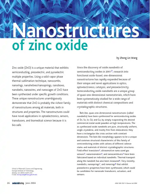
Since the discovery of oxide nanobelts of semiconducting oxides in 20011, research into functional oxide-based, one-dimensional nanostructures has rapidly expanded because of their unique and novel applications in optics,optoelectronics, catalysis, and piezoelectricity.Semiconducting oxide nanobelts are a unique group of quasi-one-dimensional nanomaterials, which have been systematically studied for a wide range of materials with distinct chemical compositions and crystallographic structures.Belt-like, quasi-one-dimensional nanostructures (called nanobelts) have been synthesized for semiconducting oxides of Zn, Sn, In, Cd, and Ga, by simply evaporating the desired commercial metal oxide powders at high temperatures. The as-synthesized oxide nanobelts are pure, structurally uniform,single-crystalline, and mostly free from dislocations; they have a rectangular-like cross-section with constantdimensions. The belt-like morphology appears to be a unique and common structural characteristic of this family of semiconducting oxides with cations of different valence states and materials of distinct crystallographic structures.Field-effect transistors 2, ultrasensitive nano-sized gassensors 3, nanoresonators 4, and nanocantilevers 5have been fabricated based on individual nanobelts. Thermal transport along the nanobelt has also been measured 6. Very recently,nanobelts, nanosprings 7, and nanorings 8that exhibitpiezoelectric properties have been synthesized, which could be candidates for nanoscale transducers, actuators, and sensors.by Zhong Lin WangNanostructuresof zinc oxideSchool of Materials Science and Engineering, Georgia Institute of Technology, Atlanta, GA 30332-0245 USAE-mail: zhong.wang@June 200426ISSN:1369 7021 © Elsevier Ltd 2004Zinc oxide (ZnO) is a unique material that exhibits semiconducting, piezoelectric, and pyroelectric multiple properties. Using a solid-vapor phase thermal sublimation technique, nanocombs,nanorings, nanohelixes/nanosprings, nanobows,nanobelts, nanowires, and nanocages of ZnO have been synthesized under specific growth conditions.These unique nanostructures unambiguouslydemonstrate that ZnO is probably the richest family of nanostructures among all materials, both in structures and properties. The nanostructures could have novel applications in optoelectronics, sensors,transducers, and biomedical science because it is bio-safe.REVIEW FEATUREAmong the functional oxides with perovskite, rutile, CaF 2,spinel, and wurtzite structures 9, ZnO is unique because it exhibits dual semiconducting and piezoelectric properties.ZnO is a material that has diverse structures, whose configurations are much richer than any knownnanomaterials including carbon nanotubes. Using a solid-state thermal sublimation process and controlling the growth kinetics, local growth temperature, and the chemical composition of the source materials, a wide range ofnanostructures of ZnO have been synthesized (Fig. 1). This review focuses on the formation of nanohelixes, nanobows,nanopropellers, nanowires, and nanocages of ZnO.Nanohelixes/nanosprings and seamless nanoringsThe wurtzite structure family has a few important members,such as ZnO, GaN, AlN, ZnS, and CdSe, which are importantmaterials for applications in optoelectronics, lasing, and piezoelectricity. The two important characteristics of the wurtzite structure are the noncentral symmetry and polar surfaces. The structure of ZnO, for example, can be described as a number of alternating planes composed of tetrahedrally coordinated O 2-and Zn 2+ions, stacked alternately along the c -axis (Fig. 2a ). The oppositely charged ions produce positively charged (0001)-Zn and negatively charged(0001)-O polar surfaces, resulting in a normal dipole moment and spontaneous polarization along the c -axis, as well as a divergence in surface energy.By adjusting the raw materials with the introduction of impurities, such as In, we have synthesized a nanoring structure of ZnO (Fig. 2)8. High-magnification scanning electron microscopy (SEM) images clearly show the perfect circular shape of the complete ring, with uniform shape andflat surfaces. Transmission electron microscopy (TEM) imagesFig. 1 A collection of nanostructures of ZnO synthesized under controlled conditions by thermal evaporation of solid powders. Most of the structures presented can be produced with 100%purity.June 200427indicate that the nanoring is a single-crystal entity with a circular shape. The single-crystal structure referred to here means a complete nanoring made of a single-crystalline ribbon bent evenly at the curvature of the nanoring. Thenanoring is the result of coaxial, uniradius, epitaxial coiling of a nanobelt.The growth of nanoring structures can be understood by considering the polar surfaces of the ZnO nanobelt. The polar nanobelt, which is the building block of the nanoring, growsalong [1010], with side surfaces ±(1210) and top/bottom surfaces ±(0001), and has a typical width of ~15 nm and thickness of ~10 nm. The nanobelt has polar charges on its top and bottom surfaces (Fig. 2b ). If the surface charges are uncompensated during growth, the nanobelt may tend to fold itself, as it lengthens, to minimize the area of the polar surface. One possible way is to interface the positively charged (0001)-Zn plane (top surface) with the negatively charged (0001)-O plane (bottom surface), resulting in neutralization of the local polar charges and reduction of the surface area, thus forming a loop with an overlapped end (Fig. 2b ). The radius of the loop may be determined by the initial folding of the nanobelt during early growth, but the size of the loop cannot be too small to reduce the elastic deformation energy. The total energy involved in the process comes from the polar charges, surface area, and elasticdeformation. The long-range electrostatic interaction is likely to be the initial driving force for the folding of the nanobelt to form the first loop for subsequent growth. As the growth continues, the nanobelt may be naturally attracted onto the rim of the nanoring because of electrostatic interactions and may extend parallel to the rim of the nanoring to neutralize the local polar charge and reduce the surface area. This results in the formation of a self-coiled, coaxial, uniradius,multilooped nanoring structure (Fig. 2c ). The self-assembly is spontaneous, which means that the self-coiling along the rim proceeds as the nanobelt grows. The reduced surface areaREVIEW FEATUREJune 200428Fig. 2 Seamless single-crystal nanorings of ZnO. (a) Structure model of ZnO, showing the ±(0001) polar surfaces. (b-e) Proposed growth process and corresponding experimental results showing the initiation and formation of the single-crystal nanoring via the self-coiling of a polar nanobelt. The nanoring is initiated by folding a nanobelt into a loop with overlapped ends as a result of long-range electrostatic interactions among the polar charges; the short-range chemical bonding stabilizes the coiled ring structure; and the spontaneous self-coiling of the nanobelt is driven by minimization of the energy contributed by polar charges, surface area, and elastic deformation. (f) SEM images of the as-synthesized, single-crystal ZnO nanoring. (g) The ‘slinky’ growth model of the nanoring. (h) The charge model of an α-helix protein, in analogy to the charge model of the nanobelt during the self-coiling process.REVIEWFEATUREFig. 3 (a) Model of a polar nanobelt. Polar-surface-induced formation of (b) nanorings, (c) nanospirals, and (d) nanohelixes of ZnO and their formation processes.June 200429and the formation of chemical bonds (short-range forces)between the loops stabilize the coiled structure. The width of the nanoring increases as more loops wind along thenanoring axis, and all remain in the same crystal orientation (Fig. 2d ). Since the growth is carried out in a temperature region of 200-400°C, ‘epitaxial sintering’ of the adjacent loops forms a single-crystal cylindrical nanoring structure,and the loops of the nanobelt are joined by chemical bonds into a single entity (Fig. 2e ). A uniradius, perfectly aligned coiling is energetically favorable because of the complete neutralization of the local polar charges inside the nanoring (Fig. 2f ) and the reduced surface area. This is the ‘slinky’growth model of the nanoring shown in Fig. 2g . The charge model of the nanoring is analogous to the α-helix protein molecule (Fig. 2h ).We have recently synthesized ZnO nanobelts that are dominated by the (0001) polar surface 7. The nanobelt grows along [2110] (the a -axis), with its top/bottom surfaces thinness (5-20 nm) and large aspect ratio (~1:4), theflexibility and toughness of the nanobelts is extremely high. A polar-surface-dominated nanobelt can be approximated to be a capacitor with two parallel charged plates (Fig. 3a ). The polar nanobelt tends to roll over into an enclosed ring to reduce the electrostatic energy (Fig. 3b ). A spiral shape can also reduce the electrostatic energy (Fig. 3c ). The formation of the nanorings and nanohelixes can be understood from the nature of the polar surfaces. If the surface charges are uncompensated during the growth, the spontaneouspolarization induces electrostatic energy as a result of the dipole moment. But rolling up to form a circular ring would minimize or neutralize the overall dipole moment, reducing the electrostatic energy. On the other hand, bending the nanobelt produces elastic energy. The stable shape of the nanobelt is determined by the minimization of the total energy contributed by spontaneous polarization and elasticity.If the nanobelt is rolled uniradially loop-by-loop, the repulsive force between the charged surfaces stretches the nanohelix, while the elastic deformation force pulls the loops together; the balance between the two forms thenanohelix/nanospring shown in Fig. 3d . The nanohelix has a uniform shape with a radius of ~500-800 nm and evenly distributed pitches. Each is made of a uniformly deformed single-crystal ZnO nanobelt.The striking new feature of the nanorings and nanohelixes of single-crystalline ZnO nanobelts reported here is that they are spontaneous-polarization-induced structures, the result ofa 90° rotation in polarization. These are ideal objects for understanding piezoelectricity and polarization-induced phenomena at the nanoscale. The piezoelectric nanobelt structures could also be used as nanoscale sensors, transducers, or resonators.Aligned nanopropellersModifying the composition of the source materials can drastically change the morphology of the grown oxide nanostructure. We used a mixture of ZnO and SnO2powders in a weight ratio of 1:1 as the source material to grow a complex ZnO nanostructure10,11. Fig. 4a is an SEM image of the as-synthesized products showing a uniform feature consisting of sets of central axial nanowires, surrounded by radially oriented ‘tadpole-like’ nanostructures. The morphology of the string appears like a ‘liana’, while the axial nanowire is like ‘rattan’, which has a uniform cross-section with dimensions in the range of a few tens of nanometers. The tadpole-like branches have spherical balls at the tips (Fig. 4a), and the branches display a ribbon shape. The ribbon branches have a fairly uniform thickness, and their surfaces are rough with steps. Secondary growth on the ‘propeller’surface leads to aligned nanowires (Fig. 4b).It is known that SnO2can decompose into Sn and O2at high temperature, thus the growth of the nanowire-nanoribbon junction arrays is the result of the vapor-liquid-solid (VLS) growth process, in which Sn catalyst particles are responsible for initiating and leading the growth of ZnO nanowires and nanoribbons. The growth of the novel structures presented here can be separated into two stages. The first stage is fast growth of the ZnO axial nanowire along [0001] (Fig. 4c). The growth rate is so high that a slow increase in the size of the Sn droplet has little influence on the diameter of the nanowire, thus the axial nanowire has a fairly uniform shape along the growth direction. The second stage is the nucleation and epitaxial growth of nanoribbons as a result of the arrival of tiny Sn droplets onto the ZnO nanowire surface (Fig. 4d). This stage is much slower than the first one because the lengths of the nanoribbons are uniform and much shorter than that of the nanowire. Since Sn is in a liquid state at the growth temperature, it tends to adsorb the newly arriving Sn species and grows into a larger size particle (i.e. coalesces). Therefore, the width of the nanoribbon increases as the size of the Sn particle at the tip becomes larger, resulting in the formation of the tadpole-like structure observed in the TEM (Fig. 4e). The Sn liquid droplets deposited onto the ZnO nanowire lead to the simultaneous growth of ZnO nanoribbons along six equivalent growth directions: ±[1010], ±[0110], and ±[1100]. Secondary growth along [0001] results in the growth of aligned nanowires on the surfaces of the propellers (Fig. 4f).Patterned growth of aligned nanowires The growth of patterned and aligned one-dimensional nanostructures is important for applications in sensing2,3, optoelectronics, and field emission12,13. Aligned growth of ZnO nanorods has been successfully achieved on a solid substrate via the VLS process with the use of Au14,15andSn16as catalysts, which initiate and guide the growth. The epitaxial orientation relationship between the nanorods and the substrate leads to aligned growth. Other techniques that do not use catalysts, such as metalorganic vapor-phase epitaxial growth17, template-assisted growth12, and electrical field alignment18have also been employed for the growth of vertically aligned ZnO nanorods. Huang et al.have demonstrated a technique for growing periodically arranged carbon nanotubes using a catalyst pattern produced from aREVIEW FEATUREJune 200430Fig. 4 Nanopropeller arrays of ZnO. (a) SEM image of Sn-catalyzed growth of aligned nanopropellers based on the six equivalent crystallographic directions. (b) Secondary growth of nanowires on the surface of the nanopropellers. (c-f) Growth process of the nanopropellers.REVIEW FEATUREmask and self-assembled submicron spheres 19. We have combined this self-assembly-based mask technique with the surface epitaxial approach to grow large-area hexagonal arrays of aligned ZnO nanorods 20.The synthesis process involves three main steps. The hexagonally patterned ZnO nanorod arrays are grown on a single-crystal Al 2O 3substrate on which patterned Au catalyst particles have been dispersed. First, a two-dimensional, large-area, self-assembled and ordered monolayer of submicron polystyrene spheres is introduced onto the single-crystal Al 2O 3substrate (Fig. 5a ). Second, a thin layer of Au particles is deposited onto the self-assembled monolayer; the spheres are then etched away, leaving a patterned Au catalyst array (Fig. 5b ). Finally, nanowires are grown on the substrate using the VLS process (Fig. 5c ). The spatial distribution of the catalyst particles determines the pattern of the nanowires.This step can be achieved using a variety of masktechnologies for producing complex configurations. Bychoosing the optimum match between the substrate lattice and the nanowires, the epitaxial orientation relationshipbetween the nanowire and the substrate results in the aligned growth of nanowires normal to the substrate. The distribution of the catalyst particles defines the location of the nanowires, and the epitaxial growth on the substrate results in the vertical alignment.Mesoporous single-crystal nanowiresPorous materials have a wide variety of applications in bioengineering, catalysis, environmental engineering, and sensor systems because of their high surface-to-volume ratio.Normally, most of these mesoporous structures arecomposed of amorphous materials and porosity is achieved by solvent-based organic or inorganic reactions. There are few reports of mesoporous structures based on crystalline material.We have reported a novel wurtzite ZnO nanowire structure that is a single crystal but is composed ofmesoporous walls/volumes 21. The synthesis is based on a modified solid-vapor process. Fig. 6a shows an SEM image of the as-synthesized ZnO nanowires grown on a Si substrate coated with a thin layer of Sn catalyst. The typical length ofthe nanowires varies from 100 µm to 1 mm and the diameterFig. 5 Growth of patterned and aligned ZnO nanowires. (a) Self-assembled monolayer of polystyrene spheres that serves as a mask. (b) Hexagonally patterned Au catalyst on the substrate. (c) Aligned ZnO nanowires grown on a single-crystal alumina substrate in a honeycomb pattern defined by the catalyst mask.June 200431Fig. 6 Mesoporous, single-crystal ZnO nanowires. (a) SEM image of high-porosity ZnO nanowires grown on an Sn-coated Si substrate. (b) High-magnification SEM images showing the morphology of a single nanowire. (c) Low-magnification TEM image of a porous ZnO nanowire and corresponding electron diffraction pattern, showing that the ZnO porous wire is covered by a thin layer of Zn 2SiO 4.is in the range of 50-500 nm. The porous structure of the ZnO nanowires is apparent (Fig. 6b ). A corresponding electron diffraction pattern from the nanowire presents two sets ofZn 2with a standard deviation of ±1.5 nm, indicating a very good size uniformity.To examine size-induced quantum effects in the ultrathin ZnO nanobelts, photoluminescence (PL) measurements were performed at room temperature using an Xe lamp with an excitation wavelength of 330 nm (Fig. 7b ). In comparison with the PL measurements from nanobelts with an average width of ~200 nm, the 6 nm nanobelts show a 14 nm shift in the emission peak, which possibly indicates quantumconfinement arising from the reduced size of the nanobelts.Polyhedral cagesCages of ZnO have also been synthesized at a high yield and purity 23. The mesoporous-structured polyhedral drum and spherical cages and shells are formed by textured self-assembly of ZnO nanocrystals, which are made by a novel self-assembly process during epitaxial surface oxidation (Fig. 8) The cages and shells exhibit unique geometricalnanostructures has been grown. It canREVIEW FEATUREJune 200432Fig. 7 Ultra-narrow ZnO nanobelts. (a) TEM image of a ZnO nanobelt grown using a Sn thin-film catalyst. (b) PL spectra of the wide (W = 200 nm) and narrow nanobelts (W = 6 nm), showing the blue shift in the emission peak as a result of size effects.REVIEW FEATUREbe predicted that ZnO is probably the richest family of nanostructures among all one-dimensional nanostructures,including carbon nanotubes.ZnO has three key advantages. First, it is semiconductor,with a direct wide band gap of 3.37 eV and a large excitation binding energy (60 meV). It is an important functional oxide,exhibiting near-ultraviolet emission and transparentconductivity. Secondly, because of its noncentral symmetry,ZnO is piezoelectric, which is a key property in building electromechanical coupled sensors and transducers. Finally,ZnO is bio-safe and biocompatible, and can be used forbiomedical applications without coating. With these three unique characteristics, ZnO could be one of the mostimportant nanomaterials in future research and applications.The diversity of nanostructures presented here for ZnOshould open up many fields of research in nanotechnology. MTAcknowledgmentsThanks to Y. Ding, P. X. Gao, W. L. Hughes, X. Y. Kong, C. Ma, D. Moore, Z. W. Pan,C. J. Summers, X.D. Wang, and Y. Zhang for helpful discussion and their contributions to the work reviewed in this article. We acknowledge generous support by the Defense Advanced Projects Research Agency, National Science Foundation, and NASA.June 200433REFERENCES1.Pan, Z. W., et al ., Science (2001) 291, 19472.Arnold, M. S., et al., J. Phys. Chem. B (2003) 107(3), 659ini, E., et al., Appl. Phys. Lett.(2002) 81(10), 18694.Bai, X. D., et al., Appl. Phys. Lett.(2003) 82(26), 48065.Hughes, W. L., and Wang, Z. L., Appl. Phys. Lett.(2003) 82(17), 28866.Shi, L., et al., Appl. Phys. Lett.(2004) 84(14), 26387.Kong, X. Y., and Wang, Z. L., Nano Lett.(2003) 3(12), 16258.Kong, X. Y., et al., Science (2004) 303, 13489.Wang, Z. L., and Kang, Z. C., Functional and Smart Materials – StructuralEvolution and Structure Analysis , Plenum Press, New York, (1998)10.Gao, P. X., and Wang, Z. L., J. Phys. Chem. B (2002) 106(49), 1265311.Gao, P. X., and Wang, Z. L., Appl. Phys. Lett.(2004) 84(15), 288312.Liu, C., et al., Adv. Mater.(2003) 15(10), 83813.Bai, X. D., et al., Nano Lett.(2003) 3(8), 114714.Yang, P. D., et al., Adv. Funct. Mater.(2002) 12(5), 32315.Zhao, Q. X., et al., Appl. Phys. Lett.(2003) 83(1), 16516.Gao, P. X., et al., Nano Lett.(2003) 3(9), 131517.Park, W. I., et al., Appl. Phys. Lett.(2002) 80(22), 423218.Harnack, O., et al., Nano Lett.(2003) 3(8), 109719.Huang, Z. P., et al., Appl. Phys. Lett.(2003) 82(3), 46020.Wang, X. D., et al., Nano Lett.(2004) 4(3), 42321.Wang, X. D., et al., Adv. Mater.(2004), in press 22.Wang, X. D., et al., J. Phys. Chem. B (2004), in press23.Gao, P. X., and Wang, Z. L., J. Am. Chem. Soc.(2003) 125(37), 11299Fig. 8 Single-crystalline, polyhedral cages and shells of ZnO.。
纳米氧化锌(性能表征、形态、表面改性)纳米氧化锌粒径介于1-100 nm之间,是一种面向21世纪的新型高功能精细无机产品,表现出许多特殊的性质,如非迁移性、荧光性、压电性、吸收和散射紫外线能力等,利用其在光、电、磁、敏感等方面的奇妙性能,可制造气体传感器、荧光体、变阻器、紫外线遮蔽材料、图像记录材料、压电材料、压敏电阻、高效催化剂、磁性材料和塑料薄膜等。
纳米氧化锌性能表征纳米级氧化锌的突出特点在于产品粒子为纳米级,同时具有纳米材料和传统氧化锌的双重特性。
与传统氧化锌产品相比,其比表面积大、化学活性高,产品细度、化学纯度和粒子形状可以根据需要进行调整,并且具有光化学效应和较好的遮蔽紫外线性能,其紫外线遮蔽率高达98%;同时,它还具有抗菌抑菌、祛味防酶等一系列独特性能。
分析测试中心用透射电镜对产品进行了分析,纳米氧化锌粒子为球形,粒径分布均匀,平均粒径20~30纳米,所有粒子的粒径均在50纳米以下。
经3400比表面及孔径测定仪(北京金埃谱科技公司)测试,纳米氧化锌粉体的BET比表面积在35m2/g以上。
此外,通过调整制备工艺参数,还可以生产出棒状纳米氧化锌。
本产品经中国科学院微生物研究所检测鉴定,结果表明,在丰富细菌培养基中,加入0.5%~1%的纳米氧化锌,可有效抑制大肠杆菌的生长,抑菌率达99.9%以上。
纳米氧化锌形态纳米氧化锌是一种多功能性的新型无机材料,其颗粒大小约在1~100纳米。
由于晶粒的细微化,其表面电子结构和晶体结构发生变化,产生了宏观物体所不具有的表面效应、体积效应、量子尺寸效应和宏观隧道效应以及高透明度、高分散性等特点。
近年来发现它在催化、光学、磁学、力学等方面展现出许多特殊功能,使其在陶瓷、化工、电子、光学、生物、医药等许多领域有重要的应用价值,具有普通氧化锌所无法比较的特殊性和用途。
纳米氧化锌在纺织领域可用于紫外光遮蔽材料、抗菌剂、荧光材料、光催化材料等。
由于纳米氧化锌一系列的优异性和十分诱人的应用前景,因此研发纳米氧化锌已成为许多科技人员关注的焦点。
纳米氧化锌晶体概述作者姓名:00班级:00学号:*********联系方式:000000000000****************纳米氧化锌晶体概述钱学森91 马博摘要:纳米氧化锌是一种具有特异性能并且用途广泛的新材料,同时也是一种重要的基础化工原料。
本文首先介绍了纳米氧化锌晶体的基本物理和化学性质,基于这些性质,进一步阐述了纳米氧化锌在各个行业的应用。
其次,本文对纳米氧化锌的制备方法进行了较为详细和系统的介绍。
于此同时,为了对纳米氧化锌的性质进行改进,以扩大其应用领域,最后,我们又对纳米氧化锌的表面改型进行了较为深入地分析。
关键词:纳米ZnO;性质;应用;制备;改性目录1 纳米氧化性概述 (5)1.1氧化锌的基本性质 (5)1.2氧化锌晶体的结构 (5)1.3纳米氧化锌的基本性能[3] (5)1.3.1表面效应 (5)1.3.2体积效应 (5)1.3.3量子尺寸效应 (6)1.3.4宏观量子隧道效应 (6)2 纳米氧化锌的应用 (6)2.1纳米氧化锌在橡胶轮胎中的应用[6] (6)2.2纳米氧化锌在陶瓷中的应用[8] (6)2.3纳米氧化锌在防晒化妆品中的应用 (6)2.4纳米氧化锌在油漆涂料中的应用 (7)2.5纳米氧化锌在纺织中的应用 (7)2.6纳米氧化锌在催化剂和光催化剂中的应用 (7)2.7纳米氧化锌在磁性材料中的应用[5] (7)2.8作为填充剂的应用 (8)3 纳米氧化锌的制备方法 (8)3.1固相法 (8)3.1.1燃烧法[14] (8)3.1.2固相合成法[14] (8)3.2液相法 (8)3.2.1直接沉淀法 (8)3.2.2均匀沉淀法[16] (9)3.2.3并流沉淀法[17] (9)3.2.4溶胶-凝胶法[18] (9)3.2.5水热合成法[19] (10)3.2.6微乳液法[20] (10)3.3气相法[21,22] (10)3.3.1激光诱导气相沉积法 (10)3.3.2气相反应合成法 (10)3.3.3喷雾热解法 (10)3.3.4化学气相氧化法 (10)4 纳米氧化锌的表面改性 (11)4.1表面物理修饰法 (11)4.1.1表面活性剂法[24] (11)4.1.2表面沉积法 (11)4.2表面化学修饰法 (11)4.2.1酯化反应法[27] (11)4.2.2 偶联剂法[24] (11)4.2.3表面接枝改性法[28] (12)4.2.4 机械化学修饰[29] (12)4.2.5外层膜修饰 (12)4.2.6 高能量表面修饰 (12)4.2.7其它方法[30] (13)1 纳米氧化性概述1.1 氧化锌的基本性质氧化锌,俗称锌白,属六方晶系纤锌矿结构,白色或浅黄色晶体或粉末,无毒,无臭,系两性氧化物,不溶于水和乙醇,溶解于强酸和强碱,在空气中能吸收二氧化碳和水[1]。