IGBT关断过程的分析
- 格式:doc
- 大小:21.00 KB
- 文档页数:5

IGBT工作原理概述:IGBT(Insulated Gate Bipolar Transistor,绝缘栅双极晶体管)是一种高性能功率半导体器件,常用于控制和调节高电压和高电流的电力电子应用中。
本文将详细介绍IGBT的工作原理及其相关特性。
一、IGBT结构IGBT由三个主要部份组成:N型电流扩散层、P型基区和N型绝缘栅区。
它的结构类似于MOSFET和双极晶体管的结合体,具有MOSFET的高输入阻抗和双极晶体管的低导通压降特性。
二、IGBT工作原理1. 关断状态:当IGBT的栅极电压为0V时,处于关断状态。
此时,N型电流扩散层和N型绝缘栅区之间形成为了反向偏置的PN结,阻挠了电流的流动。
2. 开通状态:当给IGBT的栅极施加正向电压时,即使很小的电压也能引起电流的流动。
在开通状态下,栅极电压控制导通电流的大小。
3. IGBT的导通过程:当栅极电压高于临界电压时,电流开始从N型电流扩散层注入到P型基区,形成NPN型双极晶体管。
由于双极晶体管的放大作用,电流迅速增加。
同时,由于N型绝缘栅区的存在,栅极电压控制了电流的大小。
因此,IGBT具有较低的导通压降。
4. IGBT的关断过程:当栅极电压降低到临界电压以下时,电流开始减小。
在关断过程中,IGBT的关断速度取决于去除电荷的速度。
通常,通过施加负向电压或者短路栅极电压来加快关断速度。
三、IGBT的特性1. 高输入阻抗:由于IGBT的栅极绝缘层,其输入电流极小,因此具有高输入阻抗。
这使得IGBT可以被各种控制电路轻松驱动。
2. 低导通压降:IGBT的导通压降较低,这意味着在导通状态下能够减小功率损耗,提高效率。
3. 大功率承受能力:IGBT能够承受较高的电压和电流,适合于高功率应用,如变频器、电力传输、电动车等。
4. 快速开关速度:IGBT具有较快的开关速度,可以实现高频率的开关操作,适合于需要频繁开关的应用。
5. 温度依赖性:IGBT的导通压降和关断速度受温度影响较大。

igbt的工作原理IGBT(Insulated Gate Bipolar Transistor)是一种广泛应用于电力电子领域的功率半导体器件,它结合了场效应晶体管(MOSFET)和双极型晶体管(BJT)的优点,具有高电压、高电流和高速开关特性。
IGBT的工作原理是指其在电路中的工作方式和特性,下面将详细介绍IGBT的工作原理。
当IGBT处于关断状态时,它的栅极和集电极之间的通道是关闭的,没有电流通过。
当施加正向电压到栅极时,栅极和发射极之间形成一个PN结,使得集电极和发射极之间的通道导通,电流开始流动。
IGBT的导通过程可以分为三个阶段,开启、饱和和关断。
首先是开启阶段,当正向电压施加到栅极时,栅极和发射极之间的PN结被击穿,形成导通通道。
此时,IGBT的电流开始增加,但电压降低。
接下来是饱和阶段,当电流继续增加时,IGBT的电压降低到一个稳定的值,此时IGBT处于饱和状态。
在饱和状态下,IGBT的电压降低到很小的值,电流可以自由地通过。
最后是关断阶段,当施加负向电压到栅极时,PN结被截断,IGBT的导通通道关闭,电流停止流动。
IGBT回到关断状态,等待下一次开启。
IGBT的工作原理可以用简单的模型来描述,当栅极电压施加时,形成PN结,使得集电极和发射极之间的通道导通,电流开始流动;当栅极电压去除时,PN结截断,导通通道关闭,电流停止流动。
这种工作原理使得IGBT在电力电子领域得到广泛应用,如变频空调、电动汽车、工业控制等领域。
总的来说,IGBT的工作原理是通过控制栅极电压来控制集电极和发射极之间的通道导通和截断,从而实现电流的控制和开关。
IGBT具有高电压、高电流和高速开关特性,是电力电子领域中不可或缺的器件之一。
希望通过本文的介绍,能够让大家对IGBT的工作原理有一个更加清晰的认识。

IGBT工作原理IGBT(Insulated Gate Bipolar Transistor)是一种重要的功率半导体器件,广泛应用于高压、高频率和高电流的电力电子系统中。
本文将详细介绍IGBT的工作原理,包括结构、工作过程和特性。
一、结构IGBT由P型衬底、N+型外延区、N型沟道区、P型沟道区和N+型漏极组成。
其中,P型衬底和N+型外延区形成PN结,N型沟道区和P型沟道区形成PNP结,N+型漏极是电流输出端。
二、工作过程1. 关态:当控制端施加正向电压时,PN结正向偏置,PNP结反向偏置。
此时,P型沟道区的空穴和N型沟道区的电子被吸引到PNP结的N型区域,形成导电通道。
电流从漏极流向源极,IGBT处于导通状态。
2. 开态:当控制端施加负向电压时,PN结反向偏置,PNP结正向偏置。
此时,导电通道被截断,电流无法通过,IGBT处于截止状态。
3. 开关过程:IGBT从关态到开态的过程称为开启过程,从开态到关态的过程称为关断过程。
在开启过程中,控制端施加正向电压,PN结逐渐正向偏置,导电通道逐渐形成,电流逐渐增大。
在关断过程中,控制端施加负向电压,PN结逐渐反向偏置,导电通道逐渐截断,电流逐渐减小。
三、特性1. 高电压能力:IGBT具有较高的耐压能力,可以承受较高的电压。
这使得IGBT在高压应用中具有优势,如电力变换器、电力传输系统等。
2. 高频特性:IGBT具有较高的开关速度和频率响应,适合于高频率应用。
这使得IGBT在交流电动机驱动、变频器等领域得到广泛应用。
3. 低开启压降:IGBT的开启压降较小,能够减少功率损耗。
这使得IGBT在低功率应用中具有优势,如电源、逆变器等。
4. 温度特性:IGBT的工作温度范围较广,能够在较高的温度下正常工作。
这使得IGBT在高温环境下的电力电子系统中具有优势。
总结:IGBT是一种重要的功率半导体器件,具有高电压能力、高频特性、低开启压降和良好的温度特性。
它的工作原理基于PN结和PNP结的正向和反向偏置,通过控制端的电压来实现导通和截断。
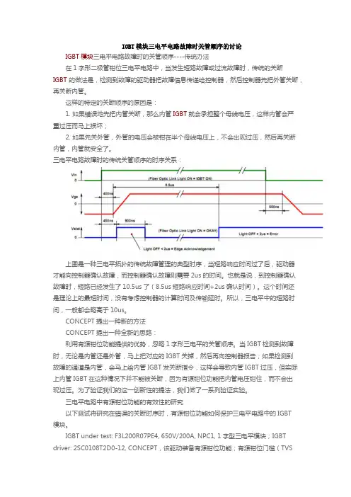
IGBT模块三电平电路故障时关管顺序的讨论IGBT模块三电平电路故障时的关管顺序----传统办法在1字形二极管钳位三电平电路中,当发生短路故障或过流故障时,传统的关断IGBT的做法是,检测到故障的驱动器把故障信息传递给控制器,然后控制器先把外管关断,再关断内管。
这样的特定的关断顺序的原因是:1. 如果错误地先把内管关断,那么内管IGBT就会承担整个母线电压,这样内管会严重过压而马上损坏;2. 如果先关外管,外管的电压会被钳在半个母线电压上,不会出现过压,然后再关断内管,内管就安全了。
三电平电路故障时的传统关管顺序的时序关系:上图是一种三电平拓扑的传统故障管理的典型时序,当短路响应时间过了后,驱动器才能向控制器确认故障,而控制器确认故障则需要2us的时间。
也就是说,到控制器确认故障时,短路已经发生了10.5us了(8.5us短路响应时间+2us确认时间)。
这个时间还是理论上的最短时间,没有考虑控制器的计算时间及传输延时。
所以,三电平中的短路时间,一般都会略高于10us。
CONCEPT提出一种新的方法CONCEPT提出一种全新的思路:利用有源钳位功能提供的优势,忽略1字形三电平的关管顺序。
当IGBT检测到故障时,无论是内管还是外管,马上把对应的IGBT关掉,然后再向控制器报告;如果检测到故障的通道是内管,会马上给内管IGBT发关断指令,这样会导致内管IGBT过压,但实际上内管IGBT在这种情况下并不能被关断,因为有源钳位功能把内管电压钳住,而不会出现过压。
为了验证我们的这一创新性的提法,我们做了一系列验证实验。
三电平电路中有源钳位功能的有效性的研究以下测试将研究在错误的关断时序时,有源钳位功能如何保护三电平电路中的IGBT模块。
IGBT under test: F3L200R07PE4, 650V/200A, NPC1, 1字型三电平模块;IGBT driver: 2SC0108T2D0-12, CONCEPT,该驱动装备有源钳位功能;有源钳位门槛(TVS击穿的典型值)设为,479V(1mA,25℃);以支持870V的最大直流母线电压Vdc(每个半直流母线电压均设为相同值以便于测量)。

IGBT工作原理引言:IGBT(Insulated Gate Bipolar Transistor)是一种功率器件,广泛应用于电力电子领域。
本文将详细介绍IGBT的工作原理,包括结构、工作过程和特点等方面的内容。
一、结构IGBT由三个主要部份组成:N型沟道区、P型基区和N型漏极区。
其中,N 型沟道区和P型基区构成PN结,而P型基区和N型漏极区构成PNP结。
IGBT的结构类似于MOSFET和普通的MOS结构,但其特殊之处在于P型基区的存在。
二、工作过程1. 关态(开关态):当IGBT的栅极电压为高电平时,栅极和N型沟道区之间形成正向偏置,使得PN结处于导通状态。
此时,电流可以从漏极流向源极,IGBT处于导通状态。
这个过程类似于MOSFET的导通过程。
2. 关断态:当IGBT的栅极电压为低电平时,栅极和N型沟道区之间形成反向偏置,使得PN结处于截止状态。
此时,电流无法从漏极流向源极,IGBT处于截止状态。
这个过程类似于MOSFET的截止过程。
3. 关断过程:当IGBT从导通状态切换到截止状态时,需要通过一定的关断过程来确保电流的截断。
这个过程中,栅极电压逐渐降低,直到PN结彻底截止。
三、特点1. 高压能力:IGBT具有较高的耐压能力,可以承受较高的电压。
这使得IGBT成为高压应用领域的理想选择,如电力电子转换器、电动汽车等。
2. 低导通压降:IGBT的导通压降较低,能够减小功率损耗,提高效率。
这使得IGBT在高频应用中具有优势,如变频器、电源等。
3. 高开关速度:IGBT具有较快的开关速度,能够实现快速的开关操作。
这使得IGBT在需要高频率开关的应用中表现出色,如逆变器、交流机电驱动器等。
4. 可靠性高:IGBT的结构设计和材料选择使其具有较高的可靠性和稳定性。
这使得IGBT 在各种恶劣环境下都能正常工作,如高温、高湿度等。
结论:IGBT作为一种重要的功率器件,具有高压能力、低导通压降、高开关速度和高可靠性等优点。

It is very common that an IGBT used for motor drive, UPS and some other industrial applications, be selected for 10 micro-second short-circuit withstand time (SCWT) if regular de-sat protection driver is used. But this driver generates high turn-off stress to the IGBT during inverter short circuit or the output becomes faulty. Under these abnor-mal conditions when the IGBT is turned-off abruptly, failures can occur if the IGBT is not selected properly. If the smart fault protection is not used, high turn-off loss will be generated and even short circuit current can ramp-up to a dangerous level destroying the IGBT. There are several ways to turn-off the IGBT once fault condition is detected. Some of these are as follows:Gate is discharged through high gate resistance. This discharge path is activated only during the above said abnormal conditions. This is not the best solution.Gate voltage is abruptly reduced to zero.Adding some source inductance which is common for both gate dis-charge path and load current.Gate de-bias occurs. But during normal condition switching loss is increased.Sense IGBT can also be used where fault current is sensed by pilot cell but the current sense accuracy of these pilot cells is not good which is further is affected by temperature.Gate voltage pattern analyzer for short-circuit protection in IGBT inverters [1]. These circuits are very sensitive to load changes and type of loads.Current sense resistor or Hall-effect devices are also used to detect fault through IGBT. But again these methods either generate power loss or are costly.But de-sat protection is the most commonly used for short-circuit and over current fault protection. De-sat detection truly provides the state of electrical over stress of IGBT under current fault condition when gate voltage is high. Reducing gate voltage in a controlled manner to just above gate threshold voltage is preferred and described in this article. This will reduce fault current and after some finite time gate voltage is brought down to zero safely, turning-off the IGBT without stress.Gate Drive CircuitThe main function of any gate driver circuit is to convert a control sig-nal to a power signal that can efficiently controls the IGBT or MOS-FET turn-on and turn-off. If the IGBT or MOSFET requires short cir-cuit protection, the gate drive circuit must safely turn-off the switch during a shorted or abnormal overload condition. A more detailed list of the gate drive circuit requirements for an IGBT or MOSFET are as follows:A controlled turn-on and turn-off of the IGBT so as to optimize the conduction and switching losses.In some applications, electrical isolation between control circuit and power circuit is very important.In the case of a short circuit condition, the IGBT should be protected and turned-off safely with minimum power dissipation and stress. The gate drive circuit should be able to minimize short circuit current and short-circuit withstand time without device failure. If both of these parameters are minimized, the power dissipation under short circuit will reduce and the system reliability will increase.During a short circuit condition, the IGBT collector to emitter voltage can rise fast. The voltage across the gate to emitter should not beIGBT Behavior under Short Circuit and Fault ProtectionUsing Two-Step-Soft-Turn-Off Gate DriverIn inverter driven UPS or motor applications, the IGBT can be destroyed when it is turned-on into a faulted motor or an output short circuit or an input bus voltage shoot through. Under these conditions current through the IGBT increases rapidly until it saturates. After fault detection, depending on the point at which the fast turn-off pulse is applied, very different levels of hole current can flow under the n+ source region, making this an important factor in the successful containment of the fault current. We present experimental observations showing that IGBT failure under short-circuit conditions is dependent on where and how the turn-off pulse is applied. A two-step (two-level) turn-off gate driver circuit is introduced which safely turns-off even a high transconductance IGBT during short-circuit and abnormal over current faults. This turn-off process startsduring faulted condition only.By Sampat Shekhawat and Bob Brockway, Fairchild SemiconductorIGBT驱动的软关断技术分析35allowed to rise due to gate to collector displacement current flowinginto the gate to emitter capacitance, Cge. Current flowing into Cge will cause Vge to rise and further increase the short circuit current.One should make sure that this condition is avoided.Preferably a totem pole output stage with separate turn-on and turn-off resistance option. The gate discharging switch of the totem pole should be as close as possible to IGBT and minimize the loop induc-tance between this switch and IGBT gate & emitter terminals. Minimize the propagation delay time between input and output pulses of the gate driver.De-SaturationThe de-saturation detection technique for identifying a short circuit and fault condition in an IGBT is well known. Generally, a de-satura-tion condition is said to exist if the voltage across the IGBT collector to emitter terminals rises above 5-8 volts while the gate to emitter voltage is high. This condition indicates that the current through the IGBT has exceeded the normal operating level. The gate drive circuit should be designed so that it reacts promptly to the short circuit and safely turns-off the IGBT within SCWT rating of the IGBT. However, in recent years, IGBTs have been designed with lower conduction and switching losses but this generally reduces SCWT. IGBT technology utilizes shallow junctions to decrease switching and conduction loss-es. However these new technologies have increased the transcon-ductance (gm) of the IGBT. Since the magnitude of the IGBT short circuit current is directly proportional to gm, during a short-circuit con-dition, a higher collector current results. The large collector current and high bus voltage place the IGBT in a state of high instantaneous power dissipation that can only be sustained for a few microseconds.The gate drive circuit must respond very quickly and efficiently to the fault current to protect the IGBT. Due to the two-step turn-off, the IGBT with even 4 microseconds short circuit withstand time can safe-ly be turned-off and protected. The IGBT, used in conjunction with the two-step turn-off gate drive, safely turns off low impedance over-cur-rent faults and shorted bus conditions where single-step gate drivers fail. The Industry standard (10 µs) SCWT is no longer required when the IGBT is used with this gate driver.IGBT Behavior during short circuit and over currentThe peak current during a short circuit is limited by the gm of the IGBT. Moreover, the rate of rise of the current is limited by the turn-on characteristics of the IGBT in combination with common emitter inductance. If IGBT collector current does not saturate and reach a state of equilibrium and bus voltage has not raised high enough attempting to turn off the IGBT during can lead to IGBT latch-up [2].In case of fault conditions very different hole current flow under n+source regions. These different hole current conditions and patterns of hole current under n+ source generate different electrical stress. In case if the gate voltage is brought down abruptly to zero before device voltage reaches clamp, the IGBT can latch-up and fail. Flow of electron through the channel is cutoff once the gate is turned off.Holes continue to inject from emitter of p-n-p structure which isknown as IGBT collector. This process stops when electrons in IGBT N-base are depleted. At this point IGBT current is almost all hole cur-rent. The amount of holes is very high here and if IGBT does not reach clamp voltage IGBT can latch-up and fail. However if enough time is allowed to complete this process and plasma of electrons in IGBT N-base is reduced or depleted so that base current reaches zero. At this point the carriers from emitter of IGBT p-n-p transistor are no longer injected and IGBT current is almost all hole current.IGBT voltage rises at a rate so that edge of the depletion spread cansweep out enough carriers to maintain inductive current. If enough time is allowed to stabilize the bus voltage while the channel current is flowing, the IGBT N-base is depleted and because of this current flow is more uniformly distributed. The displacement current becomes very small since dv/dt reduces and latch-up is avoided. If enoughtime is not allowed for the IGBT to reach clamp voltage and gate volt-age is removed abruptly, IGBT voltage will rise with high dv/dt and current in IGBT is non-uniformly distributed, high displacement cur-rent generated by high dv/dt can latch-up IGBT. Non-uniform gate ESR combined with Miller capacitance result in non-uniform turn-off of IGBT active area. This results into high localized hole current den-sity flowing laterally in P-base of parasitic n-p-n bipolar resulting in latch-up of parasitic thyristor. Because of these reasons one has to wait untill IGBT reaches clamp voltage collector current saturates. So it is safer to choose IGBT with 10 microseconds SCWT for motor drive and UPS inverter applications if a regular gate driver is used.Two step soft turn-off gate driveIt is clear that if the collector to emitter voltage rises to the DC Bus slowly and high transconductance increases short circuit current, reg-ular driver does not protect an IGBT with a low short circuit withstand time (<5us). However the longer SCWT comes at the cost of higher switching and conduction losses. The rate of rise of the collector to emitter voltage is dependent upon the operating conditions and can take several microseconds to rise to bus voltage. However, the gate drive must respond quickly to initiate turn off to protect a low SCWT IGBT. The only solution is to lower the gate voltage to just above threshold voltage of the IGBT. The IGBT reaches clamp voltage faster and reduces IGBT current during fault.The schematic of two step gate driver is shown in Figure 1. The gate driver output will produce a positive signal with respect to the IGBT emitter terminal when the control signal goes high. As the control sig-nal goes high, transistor Q1 turns on, Q2 turns off, and the LED of optocoupler U1 turns on. This forces the output voltage of the opto-coupler to the low state. When the optocoupler output goes low, both transistors Q3 and Q4 turn off, turning on the Darlington combination of transistors Q5 and Q7. This will connect the Von supply to the gate of the IGBT through the gate turn-on resistor initiating the IGBT turn-on process.During the time that transistor Q4 is off, the output stage PNP tran-sistor Q6 remains off. Once the IGBT is turned on, the inverting inputFigure 1: Two-step gate drive circuitof comparator U3 will be clamped to one diode drop (forward voltage drop of de-saturation diode DC) plus the IGBT Vcesat voltage. For the gate driver to operate properly, the inverting voltage node must be at a lower voltage level than the non-inverting voltage node. The non-inverting input voltage is set by zener diode Z2. When the con-trol signal goes low, the LED of U1 turns off, and the optocoupler out-put voltage Von goes high with respect to negative terminal of VccG.This turns on transistors Q3 and Q4. When Q3 turns on, capacitor C5discharges through R24 allowing the output of the comparator U3 to remain high. Once transistor Q4 is on, the output stage Darlington combination turns off, and the PNP transistor Q6 turns on. Now, the gate of the IGBT will discharge through R21, R22 and transistor Q6,initiating the IGBT turn-off. During normal operation (no short-circuit or overload condition) comparator U3 remains off without effecting the gate driver circuit.However, the de-saturation circuit activates when a fault occurs at the inverter output, or the complimentary IGBT turns on due to noise.When the IGBT is turned-on into the low impedance load, it draws a large current, which causes the collector to emitter voltage of the IGBT to rise towards the bus voltage. As the IGBT collector to emit-ter voltage rises, the voltage across capacitor C5 will begin to charge towards VccG.When the voltage across C5 rises above Z2 zener voltage, the com-parator U3 turns-on. When U3 turns on, the base voltage of Darling-ton transistor Q5 lowers to approximately 8 volts with some quick slope. R14, R15, R27, C6 and D2 set this voltage and slope. The applied gate voltage of the IGBT is reduced from approximately 13volts to about 8 volts, significantly decreasing the saturation current of the IGBT. As soon as the gate bias reduces, electron current (MOSFET current) reduces. As electron current reduces, base cur-rent of the IGBT structure PNP transistor reduces. Hence, the satura-tion current of the IGBT reduces.When IGBT is turned-on into an inductive short-circuit or it is under shoot through condition current ramps quickly. The voltage across the device increases and current through the IGBT saturates if the gate voltage is kept on. Now if the gate voltage is brought to zero after IGBT current saturates and drain voltage rises to clamp voltage the IGBT will turn-off safely.The Ic U4 & U5 decide the time duration of first step level voltage and after this time the comparator U2 turns on and transistor Q5 &Q7 turn-off and Q6 turns-on turning-off IGBT safely. During first step time, the collector to emitter voltage across the IGBT rises faster than it would by holding the gate at 15 volts. As previously mentioned, the faster collector to emitter voltage rise is beneficial for the IGBT to safely turn-off the IGBT under a shorted load.Figure 2 and Figure 3 depicts the Fairchild 1200V Trench IGBT turn-ing on into a resistive load and after 1 micro-second the resistor is shorted. In ‘case 1’IGBT is protected within 2.6 micro-seconds. The zener Z2 decides when to start first step. The second step voltage level is decided by D1 and Vbe of gate turn-on transistor as shown in figure 2. When the zener Z2 value is 8.2V, that allows IGBT peak cur-rent to rise up to about 300A but still it turns-off IGBT safely asshown figure 2 ‘case 1’. But in figure 3 ‘case 2’when this zener value is reduced to 5.6 volts the short circuit current only rises up to about 190A. By selecting this zener properly depending on type of IGBT technology one can reduce this short circuit peak current and increase system reliability.SummaryA new two-step gate drive circuit has been proposed which protects the IGBT during short circuit and over load fault. The gate-drive safe-ly turns-off the IGBT in two steps. The IGBT stress during short cir-cuit or fault current conditions is minimized. The new gate drive cir-cuit can safely shut-off IGBTs with SCWT as low as 3?sec. The Fairchild trench IGBT can be turned-off safely in less than 3 micro-seconds.REFERENCES[1] Jun-Bae Lee, Dac-Woong Chung and Bum-Seok Suh, “Gate Volt-age Pattern Analyzer for Short-Circuit Protection in IGBT Inverters”APEC, 2007.[2] A. Bhalla, S. Shekhawat, J. Gladish, J. Yedinak, G. Dolny, “ IGBT Behavior During Short circuit and Fault Current Protection”ISPSD’98, pp. 245-248, June 3-6,1998.[3] B. Jayant Baliga, “Modern Power Devices” John Wiley & Sons”Figure 2: Trench IGBT (FGA25N120ANTD) into short circuit ‘case 1’Figure 3: Trench IGBT (FGA25N120ANTD) into short circuit ‘case 2’。

IGBT工作原理概述:IGBT(Insulated Gate Bipolar Transistor)是一种高压、高功率开关器件,广泛应用于工业电力电子领域。
它结合了MOSFET的高输入阻抗和BJT的低导通压降,具有低开关损耗和高开关速度的优点。
本文将详细介绍IGBT的工作原理。
1. IGBT结构:IGBT由P型衬底、N型衬底和P型上层构成。
其中,N型衬底被分为N+区和N-区,P型上层被分为P+区和P-区。
N+区和P+区分别作为漏极和源极,N-区和P-区形成P-N结,是IGBT的主导电流区域。
2. IGBT工作原理:当IGBT的栅极施加正向电压时,栅极结与源极结之间形成正向偏置,使N-区的空间电荷区域扩展,导致P-N结区域的电导增加。
此时,IGBT处于导通状态,漏极和源极之间形成低阻抗通路,电流可以流过。
3. IGBT关断过程:当IGBT的栅极施加负向电压时,栅极结与源极结之间形成反向偏置,使N-区的空间电荷区域收缩,导致P-N结区域的电导减小。
此时,IGBT处于关断状态,漏极和源极之间形成高阻抗断路。
为了加速IGBT的关断过程,通常会在栅极上施加负向脉冲。
4. IGBT的三个工作区域:IGBT的工作可以分为三个区域:饱和区、过渡区和截止区。
- 饱和区:当栅极电压高于临界电压时,IGBT处于饱和区。
此时,漏极和源极之间的电阻很低,电流可以自由流动。
- 过渡区:当栅极电压在临界电压附近时,IGBT处于过渡区。
此时,漏极和源极之间的电阻会逐渐增加,电流流动受到一定限制。
- 截止区:当栅极电压低于临界电压时,IGBT处于截止区。
此时,漏极和源极之间的电阻非常高,电流无法流动。
5. IGBT的优点:- 低导通压降:IGBT的导通压降比MOSFET低,可以减小功率损耗。
- 高开关速度:IGBT的开关速度比BJT快,可以提高系统响应速度。
- 高输入阻抗:IGBT的输入阻抗比MOSFET高,可以减小驱动功耗。
- 高耐压能力:IGBT可以承受较高的电压,适合于高压应用场景。

IGBT工作原理概述:IGBT(Insulated Gate Bipolar Transistor)是一种高压、高电流功率开关器件,广泛应用于电力电子领域。
本文将详细介绍IGBT的工作原理,包括结构、工作模式和特性分析。
一、结构:IGBT由PNP型晶体管和NPN型晶体管组成,两个晶体管共享一个N型区域,中间被一个绝缘层隔开。
晶体管的结构使得IGBT既具有MOSFET的高输入电阻特性,又具有Bipolar Transistor的高电流承载能力。
二、工作模式:1. 关断状态:IGBT的控制极(Gate)施加负电压,使得P型区域与N型区域之间形成反向偏置,导致晶体管的PN结截断,IGBT处于关断状态。
2. 开通状态:IGBT的控制极施加正电压,形成正向偏置,使得P型区域与N型区域之间形成导通通道。
此时,通过控制极的电流可以控制IGBT的导通和截断。
三、工作原理:1. 开通过程:当控制极施加正电压时,形成正向偏置,P型区域的空穴和N型区域的电子会相互扩散并重新组合,形成导通通道。
同时,由于控制极的电流非常小,所以可以忽略控制极的电流对导通过程的影响。
因此,IGBT的导通主要由两个PN结之间的电压来决定。
2. 关断过程:当控制极施加负电压时,形成反向偏置,导致PN结截断。
此时,由于控制极的电流非常小,所以可以忽略控制极的电流对截断过程的影响。
因此,IGBT的截断主要由两个PN结之间的电压来决定。
四、特性分析:1. 低开通电压降:IGBT的开通电压降(VCEsat)非常低,通常在1-2V之间。
这意味着在导通状态下,IGBT可以承受较低的功耗。
2. 高电流承载能力:由于IGBT具有双极型晶体管的结构,因此具有较高的电流承载能力。
普通来说,IGBT的电流承载能力可达几百安培至几千安培。
3. 快速开关速度:IGBT的开关速度较快,通常在数十纳秒至几微秒之间。
这使得IGBT在高频率应用中具有优势。
4. 温度敏感性:IGBT的导通电压降和截断电压升会随着温度的变化而变化。
It is very common that an IGBT used for motor drive, UPS and some other industrial applications, be selected for 10 micro-second short-circuit withstand time (SCWT) if regular de-sat protection driver is used. But this driver generates high turn-off stress to the IGBT during inverter short circuit or the output becomes faulty. Under these abnor-mal conditions when the IGBT is turned-off abruptly, failures can occur if the IGBT is not selected properly. If the smart fault protection is not used, high turn-off loss will be generated and even short circuit current can ramp-up to a dangerous level destroying the IGBT. There are several ways to turn-off the IGBT once fault condition is detected. Some of these are as follows:Gate is discharged through high gate resistance. This discharge path is activated only during the above said abnormal conditions. This is not the best solution.Gate voltage is abruptly reduced to zero.Adding some source inductance which is common for both gate dis-charge path and load current.Gate de-bias occurs. But during normal condition switching loss is increased.Sense IGBT can also be used where fault current is sensed by pilot cell but the current sense accuracy of these pilot cells is not good which is further is affected by temperature.Gate voltage pattern analyzer for short-circuit protection in IGBT inverters [1]. These circuits are very sensitive to load changes and type of loads.Current sense resistor or Hall-effect devices are also used to detect fault through IGBT. But again these methods either generate power loss or are costly.But de-sat protection is the most commonly used for short-circuit and over current fault protection. De-sat detection truly provides the state of electrical over stress of IGBT under current fault condition when gate voltage is high. Reducing gate voltage in a controlled manner to just above gate threshold voltage is preferred and described in this article. This will reduce fault current and after some finite time gate voltage is brought down to zero safely, turning-off the IGBT without stress.Gate Drive CircuitThe main function of any gate driver circuit is to convert a control sig-nal to a power signal that can efficiently controls the IGBT or MOS-FET turn-on and turn-off. If the IGBT or MOSFET requires short cir-cuit protection, the gate drive circuit must safely turn-off the switch during a shorted or abnormal overload condition. A more detailed list of the gate drive circuit requirements for an IGBT or MOSFET are as follows:A controlled turn-on and turn-off of the IGBT so as to optimize the conduction and switching losses.In some applications, electrical isolation between control circuit and power circuit is very important.In the case of a short circuit condition, the IGBT should be protected and turned-off safely with minimum power dissipation and stress. The gate drive circuit should be able to minimize short circuit current and short-circuit withstand time without device failure. If both of these parameters are minimized, the power dissipation under short circuit will reduce and the system reliability will increase.During a short circuit condition, the IGBT collector to emitter voltage can rise fast. The voltage across the gate to emitter should not beIGBT Behavior under Short Circuit and Fault ProtectionUsing Two-Step-Soft-Turn-Off Gate DriverIn inverter driven UPS or motor applications, the IGBT can be destroyed when it is turned-on into a faulted motor or an output short circuit or an input bus voltage shoot through. Under these conditions current through the IGBT increases rapidly until it saturates. After fault detection, depending on the point at which the fast turn-off pulse is applied, very different levels of hole current can flow under the n+ source region, making this an important factor in the successful containment of the fault current. We present experimental observations showing that IGBT failure under short-circuit conditions is dependent on where and how the turn-off pulse is applied. A two-step (two-level) turn-off gate driver circuit is introduced which safely turns-off even a high transconductance IGBT during short-circuit and abnormal over current faults. This turn-off process startsduring faulted condition only.By Sampat Shekhawat and Bob Brockway, Fairchild SemiconductorIGBT驱动的软关断技术分析35allowed to rise due to gate to collector displacement current flowinginto the gate to emitter capacitance, Cge. Current flowing into Cge will cause Vge to rise and further increase the short circuit current.One should make sure that this condition is avoided.Preferably a totem pole output stage with separate turn-on and turn-off resistance option. The gate discharging switch of the totem pole should be as close as possible to IGBT and minimize the loop induc-tance between this switch and IGBT gate & emitter terminals. Minimize the propagation delay time between input and output pulses of the gate driver.De-SaturationThe de-saturation detection technique for identifying a short circuit and fault condition in an IGBT is well known. Generally, a de-satura-tion condition is said to exist if the voltage across the IGBT collector to emitter terminals rises above 5-8 volts while the gate to emitter voltage is high. This condition indicates that the current through the IGBT has exceeded the normal operating level. The gate drive circuit should be designed so that it reacts promptly to the short circuit and safely turns-off the IGBT within SCWT rating of the IGBT. However, in recent years, IGBTs have been designed with lower conduction and switching losses but this generally reduces SCWT. IGBT technology utilizes shallow junctions to decrease switching and conduction loss-es. However these new technologies have increased the transcon-ductance (gm) of the IGBT. Since the magnitude of the IGBT short circuit current is directly proportional to gm, during a short-circuit con-dition, a higher collector current results. The large collector current and high bus voltage place the IGBT in a state of high instantaneous power dissipation that can only be sustained for a few microseconds.The gate drive circuit must respond very quickly and efficiently to the fault current to protect the IGBT. Due to the two-step turn-off, the IGBT with even 4 microseconds short circuit withstand time can safe-ly be turned-off and protected. The IGBT, used in conjunction with the two-step turn-off gate drive, safely turns off low impedance over-cur-rent faults and shorted bus conditions where single-step gate drivers fail. The Industry standard (10 µs) SCWT is no longer required when the IGBT is used with this gate driver.IGBT Behavior during short circuit and over currentThe peak current during a short circuit is limited by the gm of the IGBT. Moreover, the rate of rise of the current is limited by the turn-on characteristics of the IGBT in combination with common emitter inductance. If IGBT collector current does not saturate and reach a state of equilibrium and bus voltage has not raised high enough attempting to turn off the IGBT during can lead to IGBT latch-up [2].In case of fault conditions very different hole current flow under n+source regions. These different hole current conditions and patterns of hole current under n+ source generate different electrical stress. In case if the gate voltage is brought down abruptly to zero before device voltage reaches clamp, the IGBT can latch-up and fail. Flow of electron through the channel is cutoff once the gate is turned off.Holes continue to inject from emitter of p-n-p structure which isknown as IGBT collector. This process stops when electrons in IGBT N-base are depleted. At this point IGBT current is almost all hole cur-rent. The amount of holes is very high here and if IGBT does not reach clamp voltage IGBT can latch-up and fail. However if enough time is allowed to complete this process and plasma of electrons in IGBT N-base is reduced or depleted so that base current reaches zero. At this point the carriers from emitter of IGBT p-n-p transistor are no longer injected and IGBT current is almost all hole current.IGBT voltage rises at a rate so that edge of the depletion spread cansweep out enough carriers to maintain inductive current. If enough time is allowed to stabilize the bus voltage while the channel current is flowing, the IGBT N-base is depleted and because of this current flow is more uniformly distributed. The displacement current becomes very small since dv/dt reduces and latch-up is avoided. If enoughtime is not allowed for the IGBT to reach clamp voltage and gate volt-age is removed abruptly, IGBT voltage will rise with high dv/dt and current in IGBT is non-uniformly distributed, high displacement cur-rent generated by high dv/dt can latch-up IGBT. Non-uniform gate ESR combined with Miller capacitance result in non-uniform turn-off of IGBT active area. This results into high localized hole current den-sity flowing laterally in P-base of parasitic n-p-n bipolar resulting in latch-up of parasitic thyristor. Because of these reasons one has to wait untill IGBT reaches clamp voltage collector current saturates. So it is safer to choose IGBT with 10 microseconds SCWT for motor drive and UPS inverter applications if a regular gate driver is used.Two step soft turn-off gate driveIt is clear that if the collector to emitter voltage rises to the DC Bus slowly and high transconductance increases short circuit current, reg-ular driver does not protect an IGBT with a low short circuit withstand time (<5us). However the longer SCWT comes at the cost of higher switching and conduction losses. The rate of rise of the collector to emitter voltage is dependent upon the operating conditions and can take several microseconds to rise to bus voltage. However, the gate drive must respond quickly to initiate turn off to protect a low SCWT IGBT. The only solution is to lower the gate voltage to just above threshold voltage of the IGBT. The IGBT reaches clamp voltage faster and reduces IGBT current during fault.The schematic of two step gate driver is shown in Figure 1. The gate driver output will produce a positive signal with respect to the IGBT emitter terminal when the control signal goes high. As the control sig-nal goes high, transistor Q1 turns on, Q2 turns off, and the LED of optocoupler U1 turns on. This forces the output voltage of the opto-coupler to the low state. When the optocoupler output goes low, both transistors Q3 and Q4 turn off, turning on the Darlington combination of transistors Q5 and Q7. This will connect the Von supply to the gate of the IGBT through the gate turn-on resistor initiating the IGBT turn-on process.During the time that transistor Q4 is off, the output stage PNP tran-sistor Q6 remains off. Once the IGBT is turned on, the inverting inputFigure 1: Two-step gate drive circuitof comparator U3 will be clamped to one diode drop (forward voltage drop of de-saturation diode DC) plus the IGBT Vcesat voltage. For the gate driver to operate properly, the inverting voltage node must be at a lower voltage level than the non-inverting voltage node. The non-inverting input voltage is set by zener diode Z2. When the con-trol signal goes low, the LED of U1 turns off, and the optocoupler out-put voltage Von goes high with respect to negative terminal of VccG.This turns on transistors Q3 and Q4. When Q3 turns on, capacitor C5discharges through R24 allowing the output of the comparator U3 to remain high. Once transistor Q4 is on, the output stage Darlington combination turns off, and the PNP transistor Q6 turns on. Now, the gate of the IGBT will discharge through R21, R22 and transistor Q6,initiating the IGBT turn-off. During normal operation (no short-circuit or overload condition) comparator U3 remains off without effecting the gate driver circuit.However, the de-saturation circuit activates when a fault occurs at the inverter output, or the complimentary IGBT turns on due to noise.When the IGBT is turned-on into the low impedance load, it draws a large current, which causes the collector to emitter voltage of the IGBT to rise towards the bus voltage. As the IGBT collector to emit-ter voltage rises, the voltage across capacitor C5 will begin to charge towards VccG.When the voltage across C5 rises above Z2 zener voltage, the com-parator U3 turns-on. When U3 turns on, the base voltage of Darling-ton transistor Q5 lowers to approximately 8 volts with some quick slope. R14, R15, R27, C6 and D2 set this voltage and slope. The applied gate voltage of the IGBT is reduced from approximately 13volts to about 8 volts, significantly decreasing the saturation current of the IGBT. As soon as the gate bias reduces, electron current (MOSFET current) reduces. As electron current reduces, base cur-rent of the IGBT structure PNP transistor reduces. Hence, the satura-tion current of the IGBT reduces.When IGBT is turned-on into an inductive short-circuit or it is under shoot through condition current ramps quickly. The voltage across the device increases and current through the IGBT saturates if the gate voltage is kept on. Now if the gate voltage is brought to zero after IGBT current saturates and drain voltage rises to clamp voltage the IGBT will turn-off safely.The Ic U4 & U5 decide the time duration of first step level voltage and after this time the comparator U2 turns on and transistor Q5 &Q7 turn-off and Q6 turns-on turning-off IGBT safely. During first step time, the collector to emitter voltage across the IGBT rises faster than it would by holding the gate at 15 volts. As previously mentioned, the faster collector to emitter voltage rise is beneficial for the IGBT to safely turn-off the IGBT under a shorted load.Figure 2 and Figure 3 depicts the Fairchild 1200V Trench IGBT turn-ing on into a resistive load and after 1 micro-second the resistor is shorted. In ‘case 1’IGBT is protected within 2.6 micro-seconds. The zener Z2 decides when to start first step. The second step voltage level is decided by D1 and Vbe of gate turn-on transistor as shown in figure 2. When the zener Z2 value is 8.2V, that allows IGBT peak cur-rent to rise up to about 300A but still it turns-off IGBT safely asshown figure 2 ‘case 1’. But in figure 3 ‘case 2’when this zener value is reduced to 5.6 volts the short circuit current only rises up to about 190A. By selecting this zener properly depending on type of IGBT technology one can reduce this short circuit peak current and increase system reliability.SummaryA new two-step gate drive circuit has been proposed which protects the IGBT during short circuit and over load fault. The gate-drive safe-ly turns-off the IGBT in two steps. The IGBT stress during short cir-cuit or fault current conditions is minimized. The new gate drive cir-cuit can safely shut-off IGBTs with SCWT as low as 3?sec. The Fairchild trench IGBT can be turned-off safely in less than 3 micro-seconds.REFERENCES[1] Jun-Bae Lee, Dac-Woong Chung and Bum-Seok Suh, “Gate Volt-age Pattern Analyzer for Short-Circuit Protection in IGBT Inverters”APEC, 2007.[2] A. Bhalla, S. Shekhawat, J. Gladish, J. Yedinak, G. Dolny, “ IGBT Behavior During Short circuit and Fault Current Protection”ISPSD’98, pp. 245-248, June 3-6,1998.[3] B. Jayant Baliga, “Modern Power Devices” John Wiley & Sons”Figure 2: Trench IGBT (FGA25N120ANTD) into short circuit ‘case 1’Figure 3: Trench IGBT (FGA25N120ANTD) into short circuit ‘case 2’。
IGBT工作原理概述:IGBT(Insulated Gate Bipolar Transistor)是一种广泛应用于功率电子领域的半导体器件,其工作原理结合了MOSFET和双极型晶体管的特点,具备高电压驱动能力和低导通压降的优点。
本文将详细介绍IGBT的工作原理,包括结构、导通和关断过程,以及其在电力电子应用中的典型工作模式。
一、IGBT结构IGBT由P型衬底、N型绝缘栅、N型漏极和P型源极组成。
其结构与MOSFET相似,但漏极区域引入了P型材料,形成PN结,使得IGBT具备双极型晶体管的特性。
二、导通过程1. 开关状态:当IGBT的栅极电压为正值时,栅极与源极之间形成正向偏置,使得栅极-漏极之间的PN结处于正向偏置状态。
此时,漏极区域的P型材料中的空穴被N型材料中的电子注入,形成导电通道。
2. 导通过程:当外部施加正向电压时,电子从源极注入漏极区域,与空穴复合,形成导电通道。
该导电通道具备低导通压降的特性,使得IGBT能够承受高电流和高电压。
三、关断过程1. 关断状态:当IGBT的栅极电压为负值时,栅极与源极之间形成反向偏置,使得栅极-漏极之间的PN结处于反向偏置状态。
此时,漏极区域的P型材料中的空穴被源极注入,形成截断区域。
2. 关断过程:当外部施加负向电压时,电子从漏极区域流向源极,与空穴复合,截断导电通道。
IGBT的关断速度取决于电子与空穴的复合速度,以及PN结的电容特性。
四、IGBT的典型工作模式1. 开关模式:IGBT在开关模式下,栅极电压快速切换,使得IGBT能够实现高效率的功率开关。
该模式适合于频繁开关的应用,如电力电子变换器、机电驱动等。
2. 线性模式:IGBT在线性模式下,栅极电压保持稳定,使得IGBT能够承受连续电流。
该模式适合于需要稳定输出的应用,如电力放大器、线性稳压器等。
五、IGBT的应用领域IGBT广泛应用于电力电子领域,如交流变流器、直流变流器、机电驱动、电力放大器等。
IGBT工作原理概述:IGBT(Insulated Gate Bipolar Transistor)是一种高性能功率半导体器件,结合了MOSFET和双极晶体管的优点。
它具有低开关损耗、高开关速度和高电压能力等特点,广泛应用于电力电子领域。
本文将详细介绍IGBT的工作原理。
一、IGBT结构:IGBT由PNPN结构的双极晶体管和MOSFET的栅极结构组成。
它的主要部份包括N+型衬底、N型漂移区、P型区、N型区、P+型区、金属栅极和漏极等。
其中,P型区和N型区构成为了双极晶体管部份,N型漂移区和金属栅极构成为了MOSFET部份。
二、IGBT工作原理:1. 关断状态:当IGBT处于关断状态时,栅极与源极之间的电压低于阈值电压,栅极-源极结处于反向偏置状态,形成一个大的反向偏置电容。
此时,双极晶体管的集电结正向偏置,处于关断状态,没有导通电流。
2. 开通状态:当栅极与源极之间的电压高于阈值电压时,栅极-源极结反转,栅极处于正向偏置状态。
栅极电压的变化会导致栅极-漂移区结的电场分布发生变化,从而控制漂移区中的电荷分布。
当栅极电压增加时,漂移区中的电荷被吸引到栅极附近,形成一个导电通道,使得双极晶体管处于导通状态。
3. 导通状态:在IGBT导通状态下,双极晶体管的集电结正向偏置,漂移区中的电荷被栅极吸引,形成导电通道。
此时,漂移区的电阻很低,电流可以通过IGBT流过。
同时,由于MOSFET结构的存在,栅极控制电流的增加或者减少可以迅速改变漂移区的电荷分布,实现快速开关。
4. 关断过程:当栅极电压降低至阈值以下,栅极-源极结反向偏置,导致漂移区的电荷重新分布。
电荷的重新分布过程需要一定的时间,称为关断过程。
在关断过程中,IGBT的导通能力逐渐减弱,电流逐渐减小,直至彻底关闭。
三、IGBT特点:1. 高电压能力:IGBT具有高耐压能力,可承受较高的电压。
2. 低开关损耗:IGBT的开关损耗较低,能够实现高效率的功率转换。
详解IGBT开关过程IGBT的开关过程主要是由栅极电压VGE控制的,由于栅极和发射极之间存在着寄生电容艮,因此IGBT的开通与关断就相当于对CGE 进行充电与放电。
假设IGBT初始状态为关断状态,即VGE为负压VGC-,后级输出为阻感性负载,带有续流二极管。
由于寄生参数以及负载特性的影响,IGBT的实际开通与关断过程比较复杂,如图1为IGBT的开通关断过程示意图,图中栅极驱动波形较为理想化,集电极电流以及集电极-发射极电压的波形大致上是实际波形,只有细节被理想化。
图1IGBT开关时间示意图表1中列出了IGBT开关时间的定义,之后是对IGBT开关各个阶段的具体介绍。
开通时间tonICBT开通时,VGE上升到0V后,VCE下降到最大值10%时为止的时间开通延时时间td(on)IGBT开通时,从集电极电流上升到最大值的10%时开始,到VCE 下降到最大值的10%为止的时间上升时间trIGBT开通时,从集电极电流上升到最大值的10%时开始,到达90%为止的时间关断时间toffIGBT关断时,从VCE下降到最大值的90%开始,到集电极电流在下降电流的切线上下降到10%为止的时间下降时间tfIGBT关断时,集电极电流从最大值的90%开始,在下降电流的切线上下降到10%为止的时间拖尾时间tt到内置二极管中的反向恢复电流消失为止所需要的时间拖尾电流It到内置二极管中正方向电流断路时反方向流动的电流的峰值表1IGBT开关时间定义1开通时间ton开通时间还可以分为两个部分:开通延迟时间td(on)与上升时间tr,在此时间内IGBT主要工作在主动区域。
当栅极和发射极之向被加上一个阶跃式的正向驱动电压后,便对CGE开始充电,VGE开始上升,上升过程的时间常数由CGE和栅极驱动网路的电阻所决定,一旦VGE达到开启电压VGE(th)后,集电极电流IC则开始上升。
从VGE上升至VGE(th)开始,到IC上升至负载电流IL的10%为止,这段时间被定义为开通延迟时间td(on)。
关断过程中栅压振荡问题应用在的高压领域中的IGBT,为了获得更优的导通压降与关断损耗的trade-off曲线,往往加入了FS层。
更高浓度的FS层和更低浓度的N-base区,可以使漂移区的电场分布从三角形阻断成梯形。
这使得获得相同耐压的情况下,硅片大大减薄,降低了制造成本。
但是,加入了FS层的IGBT的关断过程变得更加复杂,在栅压变化的影响下可能造成振荡。
图1对于高压IGBT来说,RBSOA不仅受集电极-发射极电压和集电极电流限制,同时还受最大电场强度限制。
为了能够更好地理解栅驱动条件对高压IGBT的关断影响,下面建立一维简单模型来讨论IGBT的关断过程。
1、一维关断模型对于高压IGBT来说,它的关断主要由低浓度的N-base区的大量载流子抽取决定。
在正向导通状态时,忽略了漂移区的载流子复合,同时忽略了扩散电流,只有漂移电流。
图2因此,在整个等离子区中的电子电流和空穴电流之比为迁移率之比,等于3.当栅极放电,MOS沟道减少,不再能保持电子电流。
沟道一侧开始形成空间电荷区并不断扩大,Vce升高。
电子向集电极方向流出,空穴通过空间电荷区向顶部流出,当沟道完全关闭时,整个集电极电流由流向顶部的空穴电流构成。
由泊松方程可以得到空间电荷区的电场强度梯度:()()()()x n x p N e dx x dE SCR SCR D -+=ε0,其中()()()x E v e A i x p p pSCR SCR ⋅⋅=0。
与关态时对比,空穴电流和空穴浓度为零,由于空穴电流的变化引起了一个更高的电场强度梯度,所以相同电压下会引起一个更高的最大电场强度。
这会导致动态雪崩,所以要限制高压IGBT 关断时的最大关断电流。
2、栅极驱动对关断的控制图3表示了栅极驱动对IGBT 开关的影响。
IGBT 的MOS 沟道由一个电压控制电流源代替。
等离子区的载流子抽取由电容CE C 描述,它通过SCR 区的空穴电流和等离子区的空穴电流之间的差值充放电。
IGBT驱动软关断和有源钳位技术【摘要】:由于功率回路杂散电感的存在,IGBT在关断过程中会产生过高的Vce电压尖峰,带来了IGBT损坏的风险。
本文介绍了PI公司在大功率驱动系统中常用的软关断和有源钳位技术,分析了两种电路抑制IGBT关断电压尖峰的基本工作原理和注意事项。
通过这两种技术可以有效减缓IGBT的di/dt,从而降低Vce电压尖峰,有效保护IGBT正常运行。
【关键词】:电压尖峰,软关断,有源钳位1 引言由于IGBT自身寄生电感以及主回路杂散电感的存在,IGBT在关断时,回路杂感产生的电压和母线电压叠加起来形成IGBT两端VCE电压尖峰,如图1所示:图1 IGBT换流电路及关断时Vce特性其中,为回路杂散电感产生的压降。
若是Vce电压尖峰过高,则会损坏IGBT模块。
通常可以采用软关断和有源钳位技术限制Vce电压尖峰,有效保护IGBT。
1.解决分析过程1.软关断技术软关断技术基本工作原理:如图2所示,IGBT正常关断时,选择较小的门极关断电阻以减少开关损耗;当检测到短路故障时,切换到较大的关断电阻缓慢释放门极电荷,减缓门极电压下降速度,从而减小IGBT的di/dt,降低Vce电压尖峰。
图2 IGBT软关断原理示意图图3所示为驱动板检测到IGBT短路时的软关断保护试验波形,可以看到通过软关断,电流缓慢降低,产生的Vce电压尖峰也很小,有效保护了IGBT。
图3驱动板检测到短路保护故障然而软关断电路需要检测到短路故障才能动作,这一条件在一定程度上限制了软关断的可靠性。
具体分析如下:如图4所示IGBT的开通特性,短路保护是根据IGBT开通后经过一段响应时间检测到的Vce是否大于短路门槛电压Vth反馈的。
当检测到的Vce大于Vth,则认定为短路故障;反之,正常运行。
图4 IGBT开通特性及Vce检测若是在短路情况下,是一个宽度小于响应时间的脉冲驱动信号,将检测不到短路状况,不能执行软关断,将会产生过高的Vce电压,可能损坏IGBT。
IGBT 的关断与接通都存在一些的问题关断的问题:1.关断损耗 2.关断过电压3.关断过程中微分热阻带来的局部热击穿接通的问题:1.并联ZVS电容下接入的时机 2.共态导通问题 3.反向恢复的问题借助串联谐振回路,使得IGBT 的工作条件大为改善:1. 串联全谐振变换器曾经是上世纪60-70年代最流行的变换器,只要给出合适的死区时间,即可实现很好的软开关变换. 现代的数控技术给这一经典的变换电路增添了不少活力,在控制方面解决了很多以前难以克服的困难,工程上应用它的关键技术问题有三个:. ZCS 频率追踪控制(随负载、电源漂移而调整工作频率,让换相始终处于接近零电流下的弱感性). ZVS 死区追踪控制(因负载电流不同而调整死区,实现零电压接通,接近零电压关断). ZCS_ZVS 交替追踪控制(既实现频率追踪又实现动态死区,具有良好的开关过度与调功特性)2. 关断过压问题; 既使ZVS电容较大(103),当分布电感较大时在荷载下关断,仍然会在开关上激起高于电源几百伏的浪涌电压,震荡频率大约能达到几兆,震荡衰减很快,但强烈的震荡也给开关带来了显著的额外损耗,改善的关键措施在于降低分布电感、放置较大的浪涌电流吸收电容(105-106);荷载下关断过压 1 (ZVSC=103)荷载下关断过压 2 (ZVSC=103)3. ZVS 初步设定; 假设IGBT 下降时间为180nS ,那么荷载下的过渡时间应设为多少?比如过渡时间设定为 1 - 1.5uS ,当然关断损耗比较小,但是这样的话,在空载下不能实现软过渡,看到了严重的硬开通;空载下严重的硬开通,散热器很快就烫手了(ZVSC=104)荷载下的良好过渡(ZVSC=104)荷载下的艰难过渡1 (由于过度太快,关断损耗大ZVSC=223)荷载下的艰难过渡2 (由于过度太快,关断损耗大ZVSC=223)4. ZVS 关断损耗问题在最坏情况下,初级电流波形是锯齿波,关断完全发生在最高的峰值处,IGBT的关断损耗可能达到整个开关损耗的90%以上;如果没有ZVS 过程,那么IGBT甚至没有VMOS的输出平均功率大!然而我最近不仅学会了使用ZVS过程,而且把它继续推进到了几乎让人难以置信的程度-------我将CBB474直接并联到IGBT上进行缓冲;荷载关断过程(△V 只有30V 小浪涌电压 ZVSC=474)在相同时基下的空载关断过程 (ZVSC=474)5. ZVS 下的硬接通问题; 硬接通问题是一个较难处理的问题.在没有荷载的情况下,焊机长时间工作,察看一下散热器的温度,马上就意识到问题的严重性,有时空载下居然达到了温度开关保护的程度!虽然IGBT 硬接通要比硬关断坚强地多,但是来不及散出的热量就直接威胁到了关断过程的安全.处理这一问题的关键在于实现动态死区;空载下含有很少量硬开通的过渡 1 (ZVSC=103)空载下含有很少量硬开通的过渡 2 (ZVSC=103)空载下几乎没有硬开通的过渡 2 (ZVSC=103)空载下几乎没有硬开通的过渡 3 (ZVSC=103)较好的过渡 (ZVSC=103)含有硬接通的过渡(ZVSC=103)良好的ZVS 过渡一定是线性的(ZVSC=103)6. ZVS 动态死区超越固定死区的桎喾、超越小ZVS电容的束缚,放置ZVS电容104 ,使边沿谐振的关断与接通不再残酷!空载下的慢过渡 1 (5uS) (ZVSC=104+103)荷载下的快过渡 1 (750nS) (ZVSC=104+103)空载下的慢过渡 2 (5uS) (ZVSC=104+103)荷载下的快过渡 2 (750nS) (ZVSC=104+103)7. ZVS 动态死区超越固定死区的桎喾、超越小ZVS电容的束缚,放置ZVS电容474 ,使边沿谐振的关断与接通不再残酷!动态死区可以做到25uS 以上,感亢降压模式可以极高的开关效率连续工作;良好的空载过渡 1 (ZVSC=474)良好的空载过渡 2 (ZVSC=474)良好的空载过渡 3 (ZVSC=474)荷载载过渡1 (ZVSC=474)荷载载过渡2 (ZVSC=474)相同时基下的对比----空载过渡(ZVSC=474)ZVS电压与电流的相位关系8. 串联谐振_ZVS 模式三角波电流激励负载,谐波分量高于正玄波;选择合适的隔直电容,避免发生容性换向,输出电流靠初级感亢降压抑制,借助于重ZVS 缓冲过程和动态死区控制,可实现很高的转换效率; 缺点有:1.调频范围太宽,产生一些意想不到的问题,如进入可闻声限等;2.初级有无功电流,回路利用率不够高;3.当初级电感太小时,可能因负载抖动产生很高的di/dt ,威胁到IGBT 的安全;4.一个十分重要的问题是减小流过IGBT 无功功率的问题,显然在有限容量的开关器件中存在无功分量减小了可用功率,无功电流与无功电压都是重要的因素,但是完全失去无功分量后,就不存在“软开关”了,ZVS方式减小了开关损耗,但是却没有设法减小无功功率分量;电容部分放电后的变压器(及附加电感)电压(电容206)负载回路的电流(互感器0.1A/mV)9. 串联谐振_ZCS 模式很好的正玄波电流激励负载,谐波分量最少;让电容与电感发生少量或深度的的串联谐振,换向在荷载下趋向于ZCS-ZVS ,既使只使用简单的固定死区时间,只要给出的死区余量较大,也能极大地改善IGBT 在重功率下的换向条件;这是实现重功率的主要手段,实现良好的换相条件需要谐振电容的峰值电压等于激励电压的5-7倍,震荡频率谱系很纯,频率漂移也不快,非常适合数控,相信这是当今技术条件下实现重功率变换的唯一策略;在深度谐振下的电感电压以及换向时机(输入经过100:1电压互器)在深度谐振下的电感电压与次级输出电容电压CH1:次级输出电容电压CH2:初级电感电压(输入经过100:1电压互器)频率追踪01频率追踪02频率追踪03频率追踪04频率追踪05频率追踪06频率追踪07频率追踪08频率追踪09频率追踪10频率追踪11频率追踪1210. 串联谐振ZCS_ZVS 交替追踪控制模式ZCS 频率追踪、ZVS 辅助换相、调频调功;综合了ZVS 与ZCS 的优点,适合广泛的应环境,易于调功,折衷地考虑开关损耗与谐振损耗,非常灵活;电流波形 1电流波形 2电流波形 3电压波形 1电压波形 2电压波形 311. 设计自己的嵌入性控制系统进入实验历程在串联谐振变换实验中,我一直坚持使用18V的峰值电平来驱动IGBT的开启与关闭;我的逆变实验从2003年的下半年开始,虽然经历了无数的挫折,但是我始终相信这一驱动电平没有问题,一直到现在,我还是这个观点;最近IR 新型的IGBT栅极击穿电压界限达到了30V,看来栅极驱动电压可能还要更高一些;高的驱动电压是减小导通损耗的有效手段,导通损耗热量是非常显著的,通常一个单管都达到70W以上;当然也只有在开关损耗很小的情况下才出现,否则将忙于应付开关损耗带来的可靠性问题,而无暇顾及这导通损耗了;驱动波形 1驱动波形 2实现目标的基础问题1.实现在重功率下深度谐振,降低换向时开关应力,并实施频率追踪以充分降低串联谐振回路的复阻抗来降低无功功率;2.实现在几乎所有情况下,换向时负载回路都呈感性;3.实现在不同负载下的动态死区调节,以减少空载、小载下的接通损耗;实际上难以克服的困难:1.谐振回路的问题很多a.谐振电容器发热严重,电压也很高,经常爆浆、炸裂b.电感器的绕组因趋肤效应导致异常发热严重c.电感器使用闭磁路不能实现,开磁路又对周围元件影响严重d.电感器用铁粉芯类磁芯无法连续工作e.电感器用铁氧体类磁芯太易于饱和2.当负载抖动严重时,变压器时常工作处于饱和边界之外,发出难以忍受的尖叫声音3.当需要实现的目标功率小时就很不划算:控制本身复杂、用料成本高、体积也不能做太小选择它的理由:1.重功率变换的必经之路,静电除尘、高频点焊、功率超声等唯一可选电路结构2.可靠性高3.功率可扩展性强,功率轻松扩展到兆瓦级,理由是很容易通过多个独立谐振回路多相合成,均流误差< 5%我个人的主观倾向:1.在大、中等功率下是最易于实现高可靠性的电路结构,出于可靠性考虑奋斗路程较短2.比较易于结合数控,电路结合数控后有很多特色,如调频、离散、多相合成等3.我所开发的某几种机器别无选择地应用这一结构,我也就比较熟悉一些,有亲近感4. 我看待产品设计的侧重:性能>可靠性>可扩展性>成本。
IGBT关断过程的分析
IGBT关断过程的分析上一篇,我们写了基于感性负载下,IGBT的开通过程,今天,我们就IGBT的关断过程进行一个叙述。
对于IGBT关断的可以基于很对方面进行分析,而今天我们从电压电流对IGBT的关断过程进行分析。
1前言
绝缘栅双极型晶体管(IGBT) 是双极型晶体管(BJT) 和场效应晶体管(MOSFET) 的复合器件,IGBT将BJT的电导调制效应引入到VDMOS 的高阻漂移区, 大大改善了器件的导通特性, 同时还具有MOSFET栅极输入阻抗高、开关速度快的特点。
很多情况,由于对IGBT 关断机理认识不清, 对关断时间随电压和电流的变化规律认识不清, 导致无法解释在使用过程中出现的电流拖尾长、死区时间长等现象, 不能充分发挥IGBT 的性能; 导致IGBT 因使用不当, 烧毁。
今天我们就IGBT关断时的电流和电压进行简单的叙述。
02关断机理
IGBT 结构等同于n 沟道MOSFET与pnp晶体管构成的达林顿结构, MOSFET 的漏极与pnp晶体管的基极相连。
等效电路和基本结构图如下:
IGBT的关断波形如下图所示,大致分为三个阶段:①关断延迟时间td(off);②关断过程中电压上升到10%到电流下降到90%时间Δt;③关断下降时间tf。
IGBT关断时间表达式为:
toff=td(off)+Δt +tf
ICE=IMOS+IC(BJT)=Ids+Ice
BJT 是一种电流控制型器件, 发射极e和集电极c传导的工作电流受基极b引入的较小电流的控制, 如等效电路所示, BJT受MOSFET漏极电流控制. 在IGBT关断td(off)和Δt 程中, MOSFET 的门极电压Vgs减小至Miller平台电压Vmr, 漏源电压Vds增大至Vds(max), 而漏源电流Ids保持不变. 由于Ib=Ids, BJT的集射极电流Ice受Ib控制, 所以,在IGBT关断td(off)和Δt过程中, Ice电流仍然保持不变, 如上图所示. 由上式ICE等式可知, IGBT的。