SHARP夏普EL-2128V_(中、英、日文说明书)
- 格式:pdf
- 大小:16.28 MB
- 文档页数:2


简介感谢您选择新款Sharp SH8128U 手机。
关于本用户手册本用户手册可助您快速、有效地了解手机的各项功能及操作方法。
注意•本公司郑重建议您单独存放所有重要资料的书面记录。
某些情况下,电子储存器中保存的资料可能会丢失或更改。
因此,无论因使用不当、维修、缺陷、电池更换、使用过期电池或其他任何原因而造成的资料丢失及无法使用等情况,本公司概不负责。
•对于第三方因使用本产品及其任何功能造成的经济损失或索赔,如信用卡号码被盗、储存的资料丢失或变更等,无论直接或间接原因,本公司概不负责。
•所有公司和产品名称均为其相应拥有者的商标和注册商标。
•本用户手册中的画面版式可能与实际版式有所不同。
•本用户手册中的资讯如有变更,恕不另行通知。
•并非所有网络均能支持本用户手册中描述的所有功能。
•本公司对于从网络中下载的内容及资讯概不负责。
•某些情况下,手机屏幕可能会出现一些黑点或亮点。
此现象不会对手机性能及使用产生任何影响。
简介1知识产权依照版权法规定,受版权(音乐、图片等)保护的资料的复制、变更和使用仅限于个人或私人用途。
若用户未拥有更大范围的版权或者未得到版权拥有者的明确同意而擅自复制、变更或使用以此方式制作或修订的复本,则视为违反版权法,版权拥有者有权索赔其损失。
为此,切勿非法使用受版权保护的资料。
microSDHC 及 microSD 徽标是SD-3C, LCC 公司的商标。
蓝牙®名称及徽标是 Bluetooth SIG, Inc 公司的注册商标。
Sharp 在任何情况下使用该名称都是经过授权的。
其他商标和商品名称为其各自所有者所有。
iWnn IME © OMRON SOFTWARE Co., Ltd. 2009-2010 All Rights Reserved.2简介目录简介 (1)第 1 章:入门 (9)您的手机 (9)附件 (11)安装 SIM 卡、电池和microSD卡 (11)SIM 卡 (12)电池 (12)SD卡 (14)为电池充电 (15)使用耳机 (15)打开或关闭手机 (16)第 2 章:基本介绍 (17)主屏幕 (17)解锁界面 (17)主页界面 (18)主页界面视图 (19)主页界面管理 (19)小工具界面 (20)小工具界面管理 (20)设置壁纸 (21)状态栏图标 (22)查看通知图标详细信息 (24)调整音量 (24)目录3第 3 章:通话 (26)拨打电话 (26)接听电话 (27)结束通话 (28)第 4 章:文字输入 (29)键盘视图 (30)基本输入 (31)输入选项 (31)全键盘模式/数字键盘模式 (31)设置输入法 (32)更改输入法 (32)第 5 章:通讯录 (33)添加联系人 (33)搜索联系人 (34)导入联系人 (34)导出联系人 (35)常用联系人 (36)第 6 章:信息和电子邮件 (37)文字信息 (37)创建和发送文字信息 (37)接收和管理信息 (39)多媒体信息 (42)创建和发送多媒体信息 (42)语音信息 (44)4目录首次设置电子邮件帐户 (45)添加电子邮件帐户 (46)访问电子邮件帐户 (46)编写和发送电子邮件 (47)接收电子邮件 (48)阅读和回复电子邮件 (48)管理电子邮件文件夹 (49)自定义电子邮件设置 (50)第 7 章:浏览器 (52)基本导航 (53)浏览器设置 (57)第 8 章:连接 (59)WLAN (59)蜂窝数据网络 (61)启动数据连接 (62)蓝牙 (63)第 9 章:多媒体应用程序 (65)相机 (65)拍摄图片 (65)查看拍摄的图片 (66)相机设置 (67)摄像机 (68)拍摄视频 (68)视频播放 (69)摄像机设置 (70)目录5查看图库中的图片 (71)使用图库中的图片 (72)编辑图库中的图片 (73)播放图库中的视频 (73)调用相机拍照 (73)音乐播放器 (74)音乐播放器屏幕 (74)播放音乐 (76)播放选项 (76)删除音乐库歌曲 (77)第 10 章:应用程序 (78)浏览器 (80)计算器 (80)日历 (81)相机 (82)时钟 (82)通讯录 (84)电子邮件 (84)文件管理器 (85)管理文件和文件夹 (85)图库 (86)信息 (86)音乐 (86)记事本 (87)点心新闻 (88)电子书 (89)设置 (90)6目录录音机 (91)第 11 章:管理手机 (92)手机设置 (92)无线和网络 (92)通话设置 (93)声音和显示 (93)位置和安全 (94)应用程序 (95)帐户与同步 (95)隐私权 (95)SD卡和手机内存 (96)搜索 (96)语言和键盘 (96)日期和时间 (96)设置向导 (97)关于手机 (97)基本设置 (98)日期和时间 (98)显示设置 (98)铃声设置 (99)无线设置 (100)保护手机 (101)启用或禁用 SIM 卡 PIN码 (101)重设手机 (102)备份与恢复 (103)目录7售后服务智能注册功能说明 (104)安全预防措施和使用条件 (105)索引 (111)8目录第 1 章:入门1.1您的手机1.听筒2.触摸屏3.返回键 - 按它可以返回到上一个菜单。


丨丨夏普F1CL使用说明书●复印:原稿字面朝上放好,按一下“复印”键,就可以复印出●发传真:原稿字面朝上放好,拨通对方的传真号,听到对方给的信号后,按一下“传真”给对方信号。
●收传真:听到电话响后或通完话,提起电话按一下“传真”键给对方信号。
●自动接收:留守灯不亮为自动接收。
留守灯亮为手动接收。
●振铃次数:登录—3011—输入次数—传真键—停止键返回。
●关日语:登录—3022—停止键返回。
●时间设定:登录—11—输入正确的年月日时间—传真键—停止键返回。
●音频设定:登录—142—停止键返回。
●录制留守提示:应答/消去键2次—数字1—提起电话—传真键—开始录音—录完挂电话。
●删去留守提示:应答/消去键3次—数字键1—传真键。
●将留守提示转入留守:按留守键—按#。
●留守灯亮时振铃次数:登录—2082—输入次数—传真键—停止返回。
●留守灯灭时振铃次数:登录—3011—输入次数—传真键—停止返回。
●通话录音:在通话的过程中按一下“再生/录音”键。
●播放留言或录音:按一下“再生/录音”键●删去留言或录音:按一下“应答/消去”键●扫描:取下扫描器,按一下复印键,然后压住原件匀速移动,扫描完后按一下停止键,先别放回机上,灯灭后等下会自动打印出来。
再装回●主机拨打子机:提起电话—内线/保留键—按数字键1(看是几号子机,2号就是2)。
●子机拨打主机:内线/保留键—数字键0.●子机接收传真:子机接通后按子机上”机能”键给信号特殊设定:接收自动缩小设定(节约用纸):登录----3191登录----3192为等倍比例接收放大复印:放好原稿---按"选择"键一次(功能键左边)----按复印缩小复印:放好原稿---按"选择"键两次(功能键左边)----按复印黑白反转复印:放好原稿---按"选择"键三次(功能键左边)----按复印。
REFERENCE1. ApplicationThis specification applies to the outline and characteristics of photocoupler Model No. PC817series(Lead-Free Type).2. Outline Refer to the attached sheet, page 4.3. Ratings and characteristics Refer to the attached sheet, page 5, 6.4. Reliability Refer to the attached sheet, page 7.5. Outgoing inspection Refer to the attached sheet, page 8.6. Supplement 6.1 Isolation voltage shall be measured in the following method.(1) Short between anode and cathode on the primary side and between collector and emitter on the secondary side. (2) The dielectric withstanding tester with zero-cross circuit shall be used. (3) The wave form of applied voltage shall be a sine wave.(It is recommended that the isolation voltage be measured in insulation oil.)6.2 Package specifications Refer to the attached sheet, page 9, 10.6.3 Business dealing name ("○" mark indicates business dealing name of ordered product)Ordered product Business dealing nameRank mark Ic (mA) PC817XNNSZ2B with or without2.5 to 30 PC817X1NSZ2B A 4.0 to 8.0 PC817X2NSZ2B B 6.5 to 13 PC817X3NSZ2B C 10 to 20PC817X4NSZ1BD15 to 306.4 This Model is approved by UL. (Under preparation).Approved Model No. : PC817 UL file No. : E643806.5 This Model is approved by CSA. (Under preparation).Approved Model No. : PC817 CSA approved mark " " shall be indicated on minimum unit package.6.6 This product is not designed against irradiation.This product is assembled with electrical input and output. This product incorporates non-coherent light emitting diode.6.7 ODS materialsThis product shall not contain the following materials.Also, the following materials shall not be used in the production process for this product. Materials for ODS : CFC S , Halon, Carbon tetrachloride, 1.1.1-Trichloroethane (Methyl chloroform)6.8 Specified brominated flame retardantsSpecified brominated flame retardants (PBB and PBDE) are not used in this device at all.Test conditions I F =5mAV CE =5V Ta=25℃6.9Compliance with each regulation(1) The RoHS directive(2011/65/EU)This product complies with the RoHS directive(2011/65/EU) .Object substances: mercury, lead, cadmium, hexavalent chromium, polybrominated biphenyls(PBB)and polybrominated diphenyl ethers(PBDE)(2) Content of six substances specified in Management Methods for Control of Pollution Caused by ElectronicInformation Products Regulation (Chinese : 电子信息产品污染控制管理办法).Marking Styles for the Names and Contents of the Hazardous SubstancesCategoryHazardous SubstancesLead(Pb)Mercury(Hg)Cadmium(Cd)Hexavalentchromium(Cr6+)Polybrominatedbiphenyls(PBB)Polybrominateddiphenyl ethers(PBDE)Photocoupler ○○○○○○This table is prepared in accordance with the provisions of SJ/T 11364.○:Indicates that said hazardous substance contained in all of the homogeneous materials for this part isbelow the limit requirement of GB/T 265727. NotesPrecautions for photocouplers :Attachment-1(Notice)The contents described herein are subject to change without notice for improvement since this product is under development.2. Outline3. Ratings and characteristics3.1 Absolute maximum ratings Ta=25℃Parameter Symbol Rating UnitInput *1 Forward current I F50 mA *2 Peak forward current I FM 1 A Reverse voltage V R 6 V *1 Power dissipation P 70 mWOutputCollector-emitter voltage V CEO80 V Emitter-collector voltage V ECO 6 V Collector current I c50 mA *1 Collector power dissipation P c150 mW *1 Total power dissipation P tot200 mW Operating temperature T opr-30 to +100 ℃Storage temperature T stg-55 to +125 ℃*3 Isolation voltage V iso(rms) 5 kV *4 Soldering temperature T sol270 ℃3.2 Electro-optical characteristics Ta=25℃Parameter Symbol Condition MIN. TYP. MAX. UnitInput Forward voltage V F I F=20mA - 1.2 1.4 V Peak forward voltage V FM I FM=0.5A - - 3.0 V Reverse current I R V R=4V - - 10 μA Terminal capacitance C t V=0, f=1kHz - 30 250 pFOutput Dark current I CEO V CE=50V, I F=0 - - 100 nA Collector-emitter breakdown voltage BV CEO I c=0.1mA I F=0 80 - - V Emitter-collector breakdown voltage BV ECO I E=10μA, I F=0 6 - - VTransfer charac- teristics Collector current I c I F=5mA, V CE=5V 2.5 - 30 mA Collector-emitter saturation voltage V CE(sat)I F=20mA I c=1mA - 0.1 0.2 V Isolation resistance R ISO DC500V 40 to 60%RH 5×10101011- ΩFloating capacitance C f V=0, f=1MHz - 0.6 1.0 pFCut-off frequency f cV CE=5V, I c=2mAR L=100Ω, -3dB- 80 - kHzRise time tr VCE=2V I c=2mAR L=100Ω- 4 18 μs Fall time t f- 3 18 μs*1 The derating factors of absolute maximum ratings due to ambient temperature are shown in Fig. 1 to 4. *2 Pulse width≦100μs, Duty ratio : 0.001 (Refer to Fig. 5)*3 AC for 1 min, 40 to 60%RH*4 For 10 s(Fig.1) Forward currentvs. Ambient temperature(Fig.3) Collector power dissipationvs. Ambient temperature(Fig.4) Total power dissipation vs. Ambient temperature(Fig.2) Diode power dissipation vs. Ambient temperature5040 30 20 10 00 25 75 100 -30 50 F o r w a r d c u r r e n t I F (m A )Ambient temperature Ta (℃) 125 0 0 25 75 100 20 40 60 80100 -30 50 70D i o d e p o w e r d i s s i p a t i o n P (m W )Ambient temperature Ta (℃) 125-25-25200 150 100 50 0 0255075100-30 Ambient temperature Ta (℃)C o l l e c t o r p o w e r d i s s i p a t i o n P c (m W )125250 0 025 50 75 10050 100 150 200 -30 T o t a l p o w e r d i s s i p a t i o n P t o t (m W )Ambient temperature Ta (℃)125250 -25-255555(Fig.5) Peak forward current vs. Duty ratioTa = 25℃1020 50 100 200 500 1000 2000 10-3 101010-2 -10 P e a k f o r w a r d c u r r e n t I F M (m A )Duty ratioPulse width ≦ 100μs4. ReliabilityThe reliability of products shall satisfy items listed below.Confidence level : 90% L TPD : 10 or 20Test Items Condition Failure JudgmentCriteriaSamples (n)Defective (C)Solderability 245±3ºC, 5s *2 n=11, C=0Soldering heat(Flow soldering) 270ºC, 10 sV F >U×1.2I R >U×2I CEO >U×2I C <L×0.7V CE(sat) >U×1.2U: Upper specification limitL: Lower specification limit n=11, C=0(Soldering by hand) 400ºC, 3 sTerminal strength(Tension)W eight: 5N 5 s/each terminal n=11, C=0Terminal strength(Bending) *3W eight: 2.5N 2 times/each terminal n=11, C=0Mechanical shock 15km/s2, 0.5ms3 times/±X, ±Y, ±Z directionn=11, C=0V ariable frequency vibration 100 to 2000 to 100Hz/4 min 200m/s24 times/X, Y, Z directionn=11, C=0Temperature cycling 1 cycle –55 ºC to +125 ºC(30 min) (30 min)20 cycles testn=22, C=0High temp. and highHumidity storage+85ºC, 85%RH, 1000h n=22, C=0 High temp. storage +125 ºC, 1000h n=22, C=0 Low temp. storage -55 ºC, 1000h n=22, C=0Operation life I F=50mA, P tot=200mWTa=25 ºC, 1000hn=22, C=0*1 Test method, conforms to EIAJ ED 4701.*2 The product whose not-soldered area is more than 5% for all of the dipped area,and/or whose pinholes or voids are concentrated on one place shall be judged defect. *3 Terminal bending direction is shown below.θθ5. Outgoing inspection5.1 Inspection items(1) Electrical characteristicsV F, I R, I CEO, V CE(sat), I c, R ISO, V iso(2) Appearance5.2 Sampling method and Inspection levelNote 1) Thickness : 0.5±0.2mm2) Process with applying antistatic treatment.3) Unless otherwise specified tolerances shall be ±0.5mm.(However except for deformation due to the stopper in sleeve.)6.2 Package specification6.2.2 Package method(1) MAX. 100pcs. of products shall be packaged in a sleeve ① and both of sleeve edges shall be fixed by stoppers ②. (2) MAX. 25 sleeves (Product : 2500pcs.) above shall be packaged in inner case ③. and sealed by tape ④. (3) The label ⑤ shall be put on the top of the inner bag.(4) Max 2 bags(product : 5000pcs) above shall be packaged in packing case ⑥, and put a cushioning material ⑦ inside. (5) The label ⑨ shall be put on the side of the packing case.(6) Case shall be closed with the lid and enclosed with kraft tape ⑧.6.2.3 Sleeve package ① outline dimensions(Unit :mm)10/106.2.4 Packing outer case outline dimensionsStopper ② Storage conditionPackaged products shall be stored at the temperature 5 to 30℃ and the humidity 70%RH or lessaway from direct sunlight.Precautions for Photocouplers1 Cleaning(1) Solvent cleaning : Solvent temperature 45℃or lessImmersion for 3 min or less(2) Ultrasonic cleaning : The effect to device by ultrasonic cleaning differs by cleaning bath size, ultrasonic power output,cleaning time, PCB size or device mounting condition etc. Please test it in actual using conditionand confirm that any defect doesn't occur before starting the ultrasonic cleaning.(3) Applicable solvent : Ethyl alcohol, Methyl alcohol, Isopropyl alcoholWhen the other solvent is used, there are cases that the packaging resin is eroded.Please use the other solvent after thorough confirmation is performed in actual using condition.2. Circuit design2.1 The LED used in the Photocoupler generally decreases the light emission power by operation.In case of long operation time, please design the circuit in consideration of the degradationof the light emission power of the LED. (50%/5years)2.2 There are cases that the deviation of the CTR and the degradation of the relative light emission powerof the LED increase when the setting value of I F is less than 1.0mA. Please design the circuit in consideration of this point.3. Precautions for Soldering(1) In the case of flow soldering (Whole dipping is possible)It is recommended that flow soldering should be at 270℃or less for 10 s or less(Pre-heating : 100 to 150℃, 30 to 80s).(2 times or less)(2) In the case of hand solderingWhat is done on the following condition is recommended.( 2 times or less)Soldering iron temperature : 400℃or lessTime : 3s or less(3) Other precautionsDepending on equipment and soldering conditions (temperature, Using solder etc.),the effect to the device and the PCB is different.Please confirm that there is no problem on the actual use conditions in advance.Attachment-1。

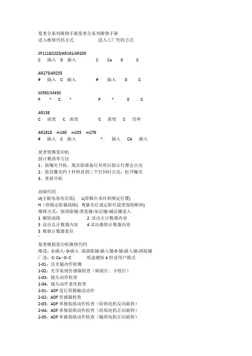
夏普全系列维修手册夏普全系列维修手册进入维修代码方式进入工厂代码方式SF1118/1025/AR161/AR200C 插入0 插入 C Ca 0 CAR275/AR255# 插入 C 插入# 插入0 CM350/M450P * C * P * 0 CAR158C 浓度 C 浓度 C 浓度 C 倍率AR2818 m160 m205 m276# 插入 C 插入* 插入CA 插入夏普便携复印机鼓计数清零方法1、按曝光开机,现在除准备灯外所以指示灯都会点亮2、按住曝光约十秒钟直到三个灯同时点亮,松开曝光3、重新开机故障代码U(主板电池电压低) L(原稿台未回到规定位置)H(热辊定影器故障) F(暴光灯或定影灯温度保险断掉)维修方式:按清除键-重复键-加法键-减法键进入1 解除故障2 读出主计数器内容3 读出总计数器内容4读出维修计数器内容5 维修计数器复位`夏普模拟复印机维修代码维进:C-插入- 0-插入或清除键-插入键-0键-插入键-清除键厂进:C- Ca - 0- C 纸盒键按4秒进用户模式1-01:反光镜动作检测1-02:光学系统传感器检查(缺纸灯、卡纸灯)1-03:镜头动作检查1-04:镜头动作老化检查2-01:ADF进行原稿输送动作2-02:ADF传感器检查2-03:ADF单独装纸动作检查(给纸电机反向旋转)2-04:ADF单独装纸动作检查(给纸电机正向旋转)2-05:ADF单独装纸动作检查(输纸电机正向旋转)2-06:ADF单独装纸动作检查(输纸电机反向旋转)2-07:ADF单独装纸动作检查(原稿限位器电磁阀接通)2-08:ADF单独装纸动作检查(送纸限位器)2-10:ADF单独装纸动作检查3-02:分页器传感器检查3-03:分页器单独装纸动作检查(输纸电机)3-04:分页器单独装纸动作检查(纸库电机)3-05:分页器单独装纸动作检查(蜂鸣器)3-06:分页器单独装纸动作检查(直线马达)(只适用于SF-S54)3-07:分页器单独装纸动作检查(钳夹马达)(只适用于SF-S54)5-01:操作面板显示检查(LED灯全亮5秒)5-02:加热灯检查(以0.5秒间隔亮灭加热灯)5-03:复印灯点亮检查5-04:DL 光度检查(放电灯亮30秒)5-05:BL 光度检查(消电灯以5秒间隔亮灭)6-01:输纸系统装纸动作(离合器/ 电磁阀)通断30次6-02:给纸电机动作检查(仅SP-2118)6-10:主纸盒半圆辊动作7-01:预热时间显示和老化预热计时并显示(秒)7-04:预热省略7-06:间歇老化7-08:预热时间显示8-01:显影偏压输出(30秒)8-02:主/ 转印充电输出/ 栅极检查(ME)8-03:主/ 转印充电输出/ 栅极检查(PE)8-04:主/ 转印充电输出/ 栅极检查(T / S)8-07:分离充电器输出(30秒)9-02 ADU传感器检查测试指令9-05 门电磁铁启动10 :色粉电机转动14 :故障消除(除U2故障外)15 废色粉装满(小人灯闪亮)取消16 U2 故障取消17 消除PF故障20-01 保养计数器(小人灯亮)清零21-01 保养周期设定0=50000张1=2500张2=5000张3=10000张4=25000张5=关闭21-02 显影器小修设置0=80000张1=5000张2=10000张21-03 彩色显影器小修设置0=10000张1=5000张22-01:保养计数器显示22-02:保养预置计数器显示22-03:卡纸存储器显示22-04:总卡纸存储器显示22-05:总计数器显示22-06:DV 计数器显示22-07:DV 预置计数器显示(载体更换周期)22-08:ADF 送纸数显示22-10:装订计数显示22-15:故障记忆显示(显示最近20个错误代码)24-01:卡纸存储器/ 总卡纸计数器清零24-02:故障记忆清除24-04:ADF 计数器清零24-05:装订计数清零24-06:显影剂调整时间清零24-07:鼓调整时间清零24-06:纸盒计数器清零25-01:主驱动系统检查25-02:自动显影剂调整(更换载体后执行)(厂代中80-2调浓度与漏粉)26-01:选购件设定(输入选购件所表数值之和)26-05:计数器方式设定( 0 A3计数 3 A4计数)26-06:目的地设定(设为10)26-07:转鼓灵敏度设定校正复印灯电压(1-3 初始为2)26-10:AE 原稿浓度设定(1低浓度原稿2正常浓度原稿)26-13:预热方式设定(0 正常1主电机转至预热结束)26-20:后缘空白设定(0 有空白1无空白)26-29:交流电压调整(0 100V 1 200V)30-01:复印机传感器检查(纸检测)42-01:清除小太阳符号换载体后43-01:定影温度设定(倍率键选择)44-01:成像控制动作设定(输入校正方式代码总和,栅压校正+1 光学尘埃校正+2 鼓磨损校正+4)44-05:栅极电压较正(显示图介浓度传感器A/D输入值)44-06:栅极电压较正强行执行44-07:图像浓度/ 转鼓标记传感器动作试验(F-J中0表示鼓标不能检测,1表示能检到)44-08:成像控制数据显示44-09:成像控制数据显示(最新值)44-10:栅极电压较正(转鼓表面/ 斑纹)数据显示44-11:初级栅极偏压设定44-12:中央控制处理器关闭时对复印功能进行检测主代码子代码内容46-01:曝光调整47 :AE 传感器增益自动调整(先在稿台上放几张A3白纸)48-01:前/ 后(垂直)放大倍率调整(A值调100% B调200% C调50%)48-02:输纸方向放大倍率调整(反光镜速度校正)50-01:复印件前缘调整50-02:前缘调整(简单型)(C值为245 显示为A45)51-02:阻力量调整(A 托盘阻力B手动给纸)53-01:ADF 停止位置调整值(普通纸)设定53-03:ADF 停止位置调整值(薄纸)设定53-04:ADF 阻力传感器、宽度传感器调整53-05:ADF出纸传感器调整53-06:ADF 时间传感器调整54-03:除去蜂鸣装置57 删边量调整58 -1 纸头调整58-2 空白区调整60 原稿尺寸检测97 补粉夏普模拟复印机故障代码L1-00:反光镜进给故障(传感器坏、主板坏、反光镜传动索缺油)L3-00:反光镜返回故障L4-01:主电机故障L5-00:镜头初始误差检测L5-02:镜头故障L5-03 第4/5反光镜电机故障L5-04 第4/5反光镜电机MHPS故障L5-05 镜头电机故障L5-06 镜头原位检测出错L5-8 镜头原位传感器故障L6 加粉电机故障L8-01:零交叉脉冲故障L8-03:AE传感器故障(执行47时,AE输入无变化)L9 分页器故障H2-00:定影热敏电阻开路故障(热敏电阻输入超过3.81V)H3-00:定影高温故障(定影温达240度,热敏电阻输入在0.36V下) H4-00:定影低温故障U1 存储器电池电压底于2.2V,指令“13”,复位U2-01:后备储存器故障U3-8 镜架驱动电机检测异常U3-10 镜架原位传感器故障U3-20 反光镜电机锁定U3-21 反光镜原始位置出错U3-40 时钟脉冲故障U4-02 ADU对位板操作错误检测U4-04 ADU后端板故障U5-00:ADF通信错误U5-01:A马达错误检测U5-03 时序传感器故障U5-04 空传感器故障U5-11:给纸电机故障U5-12:输纸电机故障U6-00:机架通信错误U6-01:1纸盒电机错误U6-02:2纸盒电机错误U6-03:3纸盒电机错误U6-08:机架24V线路出错U6-10:机架送纸电机错误U6-09:机架LCC电机过电流检测F1-00:分页器通信错误F1-02:输纸电机故障F1-04:纸库上限/下限故障F1-05:纸库原位传感器故障F1-06:纸库电机故障F1-14:输纸电势故障F2-02:色粉粉斗电机错误F2-31:图象浓度传感器故障(传感器脏、删边灯脏、鼓处插线坏)F2-32:鼓标记传感器故障F2-35:栅级电压校正故障F3-12 上纸盒升起电机故障F3-22 下纸盒升起电机故障C2 高压发生器故障电极丝短路或断路CC 原稿尺寸传感器误检测EE-EU:色粉不足EE-EL:色粉过多CH:亮是盖打开闪烁是显影组件安装不到位夏普数码复印机维修代码1-1 确认反射镜装置动作1-2 确认光学系传感器动作1-6 反光镜扫描连续动作2-1 SPF连续动作2-2 确认SPF传感器动作2-3 确认SPF电动机正转方向动人2-4 确认SPF电动机逆转方向动作2-8 确认SPF进纸电磁阀动作2-9 RSPF翻转电磁铁动作检查2-10 RSPF出纸门电磁铁动作检查2-11 确认SPF PS释放电磁阀动作3-2 确认移动分离传感器动作3-3 确认分页器移动动人3-4 确认分离板动作(检测是否正常转动)3-11 确认配页器原位动作5-1 确认扣作部显示(面板LED灯全亮秒)5-2 确认加热灯亮(定影灯50秒间隔亮5次)5-3 确认复印机灯亮(10秒浓度键改亮度)6-1 确认进纸电磁阀动作(50秒间隔驱动20次)6-10 驱动主盒半圆辊7-1 预热时间表示有JAM老化7-4 预热省略7-6 间歇老化有纸7-8 预热时间表示8-1 复印模式的显影偏压输出8-2 复印模式的主充电器栅极电压(High状态高)输出8-3 复印模式的主充电器栅极电压(Low状态低)输出8-6 转印电压输出8-10 打印模式的显影偏压以及控制回路的动作确认和调整8-11 打印模式的主充电器栅极电压(High状态)以及控制回路的动作确认8-12 打印模式的主充电器栅极电压(Low状态)以及控制回路的动作确认8-13 FAX模式的显影偏压以及控制回路的动作确认和调整8-14 FAX模式的主充电器栅极电压(High状态)以及控制回路的动作确认8-15 FAX模式的主充电器栅极电压(Low状态)以及控制回路的动作确认9-1 双面器负载(马达)正转测试9-2 双面器负载(马达)反转测试9-4 双面器马达的转速调整9-5 双面器马达的把向转换时间调整10 确认墨粉电动机动作14 解除U2以外的故障16 解除U2故障20-1 清除保养计数21-1 保养循环的设定(0=2500张1=5000张2=15000张3=30000张4=150000张5=999999张)22-1 保养计数器的显示22-2 保养预置值显示(SIM20-1设定值)22-3 卡纸储存的显示(最近30次卡纸)22-4 总卡纸计数显示22-5 总计数显示22-6 显影计数器显示22-8 SPF计数器显示22-9 进纸计数器显示22-12 光鼓计数器显示22-13 CRUM类型显示22-14 FLASH ROM的版本22-15 故障储存器显示(最近15次故障)22-16 双面打印计数显示22-17 复印计数器显示22-18 打印计数器显示22-19 电子分类计数器显示22-21 扫描计数器显示22-22 SPF卡纸计数器显示24-1 卡纸储存器清除24-2 故障储存器清除24-4 SPF计数器清除24-5 双面打印计数清除24-6 进纸计数器清除24-7 光鼓计数器清除24-8 复印计数器清除24-9 印刷计数器清除24-10 电子类计数器清除24-13 扫描计数器清除24-14 SPF卡纸计数清除24-15 扫描模式计数器清除25-1 确认主电机机劝作(30秒)25-10 确认LSU多面镜电动机动作(30秒)26-1 选件开关的显示(选购件对应灯亮)26-3 部门管理器的设定(0:计数模式1:投币模式)26-4 本机双面动作设置(0:无双面1:有双面功能)26-5 计数器方式设定(0:双面计数1:单面计数)26-6 发送地设定(5:中国6:台湾)26-7 直接显示CPM旋转速度26-10 网络扫描的试用设定26-18 节粉方式(0:节粉关闭1打开)26-22 语言设定(打印卡面板语言)(0:日语1:英语……)26-30 CE标记对应控制设定(0:CE标记OFF 1:ON)26-32 风扇旋转状况变化26-36 (0:保养计数到停机1:不停)26-37 (0:载体计数到停机1:不停)26-38 光鼓超寿命停止设定(0停机1不停机)26-39 内存容量检测(16:16M内存32:32M内存)26-42 转印时间调整(R系列:1:240MS 3:260MS 9:320MS)(M系列机子取值1-99 默认值50)26-43 上下端空白设置(自动灯表下端,手动灯表上端)26-50 黑白转换功能设定(0:可转1:不可转)26-51 复印机暂停功能设定(0:不停1:停)26-60 未装载FAX时,设定FAX模式键是否有效27-1 设定有元PC/调制解调器的通信故障27-5 输入机器的机号30-1 确认本体传感器动作30-2 确认给纸部的传感、检测器及相关回路的动作40-1 确认手动托盘的纸张尺寸检测器及相关回路的动作41-2 调整OC原稿检测传感器41-3 原稿检测传感器受光电平显示41-4 OC盖板20度时的检测电平调整42-1 载体记数清除43-1 定影温度设定(倍率键调)43-10 明信片纸张进纸周期设置(取值1-99)43-11 明信片纸定影温度设置43-12 待机模式定影风扇转动设置(0:低速1:高速)43-13 定影纸张间隙控制(0:禁止1:允许)44-34 转印电流设定44-40 墨粉补充前转动时间设置(取值1-99)46-1 复印浓度300dpi电平调整46-2 复印曝光600dpi浓度等级调整46-7 分别调整复印曝光浓度等级(超级照片)46-9 复印浓度等级单独调整手动300dpi等级(文字)46-10 复印浓度等级单独调整手动600dpi(文字/照片)46-11 复印浓度等级单独调整(照片)46-18 复印对比度调整300dpi46-19 曝光时的图像质量调整46-20 SPF的曝光浓度校正46-29 复印对比度调整600dpi46-30 进行AE设定(取值0-30)46-31 图像锐度调整(0:黑白校正2:清晰)46-39 调整传真模式对比度46-45 调整传真模式的图像浓度48-1 主(前后)扫描方向倍率调整48-2 复印时OC方式副扫描方向倍率调整48-3 自动调整前端.副扫描倍率48-5 复印时SPF方式副扫描方向倍率调整49-1 FLASH ROM程序写入模式50-1 复印画像位置调整(左右方向,值加减1移动0.127MM)50-5 调整图像先端位置50-6 调整复印模式SPF/RSPF原稿图像位置50-10 用纸中心偏移调整(上下方向)50-12 调整复印模式原稿图像中心位置50-13 OC方式原稿中心偏50-16 SPF方式原稿中心偏听偏信移调整50-18 双面复印时反面图像位置调整50-19 双面复印时后端空白调整51-02 对位量调整51-8 设定禁止感光鼓分离爪动作53-8 SPF扫描位置调整56-1 传送MFP控制器数据61-1 检测LSU的动作61-2 调复印模式激光功率(绝对值)61-3 六棱镜电机检测62-1 格式化硬盘62-3 检测硬盘读写操作62-8 格式化硬盘(除系统数据区域)62-10 删除完成作业列表(同时删除作业日志)63-1 确认黑白校正数据63-2 执行黑白校正63-7 自动调整SPF白校正开始的像素位置64-1 自我打印功能65-5 进行操作面板的检测66-22 调传真听筒音量66-23 下载传真程序66-24 清除传真数据内存66-39 设定发货地规格66-60 设定ACR数据67-11 用于设定“select-in“信号67-14 进行flash programs写入/比较检测67-17 进行NVROM的清除67-18 清除FLASH ROM 的Network Scanner Application(网络扫描应用软件)用数据区域67-20 装载网络扫描组件时,检测网络连接夏普数码复印机故障代码H2 00 热敏电阻断开(电阻到MCU板的连接、SIM14清)H3 00 定影部高温故障(温超240度、SIM5-2灯闪时:查接线。
記憶卡匣/ Nano SIM前置電源按鈕音量 (+/-)按鈕後置相機閃光燈※初次啟動裝置之前,建議先充電至少30分鐘使用盒內隨附的音頻轉接線,可將手機Type C接口轉為3.5mm耳機孔。
使用電池的安全注意事項道路及環境安全飛航安全• 本手機電池不可拆,請勿自行拆裝,若不當更換會有爆炸之危險。
• 請依照當地法規回收或處理廢棄電池。
警語智慧財產權資訊免責條款保固聲明保固範圍SHARP 提供「產品保固聲明」,針對客戶向SHARP 或授權的代理經銷商,所購買合法授權標示SHARP 產品,提供產品保固服務。
SHARP 並無提供全球維修保固服務。
產品於正常環境使用之下,因原物料及加工過程中之瑕疵而導致故障,功能無法正常使用,提供一年的保固服務,產品的保固期限自該「機器」的購買日起算,消費者須出示原始購買日之購買證明始能享有保固服務。
保固期限內,發生不在「免責條款」內的自然損壞故障,則SHARP 將提供貴客戶免費的「維修服務」,任何經過維修後的機器,依舊是以最初購買機器時的保固期限為準,並不做延長。
針對超過保固期或是人為損害的維修品,對其同一問題點,提供三個月維修保固,「維修服務」指的是對故障機器內的零件,提供一對一的零件置換動作,以恢復機器正常運作;任何被更換下來的故障零件,其資產屬於SHARP 所有;消耗性和/或消耗性物品或零件例如:除可拆卸式電池為六(6)個月保固與不可拆卸式電池為十二(12)個月保固外,其他配件限於線材、耳機、電源變壓器(若有提供者),則為六(6)個月保固。
當機器外殼上的機器序號被撕毀或被不當更改時,則該機器將無法享有保固權益。
擅自除去或更動機器序號內零件之識別標籤,則該零件亦無法享有保固權益。
當機器出現下面幾種情形時,該機器將無法享有SHARP 原廠的保固權益:(1) 經過SHARP 判斷,機器因為被不當的使用、操作疏忽、不當安裝 維護、經由非SHARP 授權之人員拆卸、維修、擅自更改產品結構 使用非SHARP 原廠所提供的零件或裝置,所導致之故障損壞。
MICROWAVE OVENRR-242EOPERATION MANUAL AND COOKBOOK1BCONTENTSPageWarning ......................................................... E-1 Special Notes ................................................ E-2 Installation Instructions ............................... E-3 Oven Diagram ............................................... E-3 Operation of Touch Control PanelControl Panel Display ................................. E-4 Touch Control Panel Layout ...................... E-4 Getting Started ........................................... E-5 Clock Setting ............................................... E-5 Stop/Clear ................................................... E-5 To Cancel a Programme During Cooking ..... E-5 Manual Operations Microwave Cooking Techniques ............... E-6 Microwave Time Cooking .......................... E-7 Sequence Cooking ..................................... E-8 Instant Cook ................................................ E-8 Increasing Time During the Cooking Programme ............... E-9 Slow Cook ................................................. E-10 Slow Cook Recipes ................................... E-11 Automatic Operations Notes for Automatic Operations ............. E-13 Auto Cook ................................................. E-13 Auto Cook Menu Guide ........................... E-14 Reheat ....................................................... E-16 Reheat Menu Guide ................................. E-16 Express Defrost ........................................ E-17 Express Defrost Menu Guide .................. E-18 Easy Defrost .............................................. E-19 Easy Defrost Menu Guide ........................ E-20 Other Convenient Features Less/More Setting .................................... E-21 Child Lock .................................................. E-22 Demonstration Mode ............................... E-22 Alarm ......................................................... E-22 Care and Cleaning ...................................... E-23 Service Call Check ...................................... E-23 Specifications ............................................. E-23 Recipes ....................................................... 1 BC–1C–214 329 11845 67416273849501 12131015A B C D EC–3COOK DEF KG QTY CHECKAUTO COOKC–41 2 1 2 3C–5C–6–––––––––––––––––––––––––––––––––––––––––––––––––––––––––––––– ––pe–––––––––––––––––––––n––––––––1COOK2COOK1COOK2 COOK x33COOKC–71COOK2 COOK x33COOKCOOK4COOK1COOKC–81COOK2 COOK x3COOK3COOK4COOKx2C–91x12COOKCOOK3C – 10C – 11C – 12QTYx2COOKC – 13C – 14C – 151 2 3rH 1 rH 2 rH 3 rH 4x2QTYCOOKQTYCOOKC – 16DEFx11COOK DEF2DEFCHECK3COOK DEFCOOK DEF4C – 171 2 3C – 181DEF KG2COOK DEF KGCOOK DEF34DEFCHECK5 COOK DEFCOOK DEF6C – 19C – 201 QTY x2x22COOK1DEF KG2COOK DEF KG3COOK DEFx14 COOK DEFC – 21C – 22C – 23RECIPESSOUPShrimp Balls and Straw Mushroom Soup[Ingredients] 230 g Shrimps 40 g Pork fat 1 can Straw mushrooms few Spring onions (strips) few Sesame oil[Seasonings](A)1 tsp Salt1/2 tsp Monosodiumglutamate1/2 tsp Pepper1Egg white1/2 tsp Cornflour(B) 1 tsp 1 tbsp 2 tsp3 cupsSalt Rice wine Monosodium glutamate Water[Method] 1. Remove veins from shrimps, drain and chop. Add porkfat and seasonings (A), stir well, to make a thick paste. Use a tablespoon to form shrimp balls. Set aside. 2. Combine seasonings (B) in large casserole. Cover and microwave at HIGH for 7 minutes. 3. Add shrimp balls, straw mushrooms and spring onions. Cover and microwave at HIGH for another 3 to 4 minutes until shrimp balls float. Sprinkle sesame oil in soup and serve.Meatballs and Tomato Soup[Ingredients] 150 g Tomatoes 150 g Ground pork 2 stalks Spring onion 2 slices Gingerfew Coriander, chopped few Celery, chopped few Sesame oil[Seasonings](A)1/2 tsp Salt1/4 tsp Monosodiumglutamate1/2 tsp Rice wine1/2 tsp Soy sauce1 tsp Cornstarch1Egg white(B) 1/2 tsp 1 stalk 1/4 tsp 1/4 tspSalt Spring onion Pepper Monosodium glutamate[Method] 1. Finely chop spring onion and ginger. Cut tomatoesinto quarters. 2. Mix ground pork with spring onion, ginger andseasonings (A), then add egg white and cornstarch, stir well. Use tablespoon to form meatballs. 3. Microwave 3 cups water and tomatoes in a large, covered bowl at HIGH for 7 minutes. Add meat balls and seasonings (B), cover, microwave at HIGH for another 3 to 4 minutes. Garnish with coriander and celery, sprinkle sesame oil before serving.1Broccoli and Minced Fish Soup[Ingredients] 300 g Fish meat 150 g Broccoli 2 tbsp Ham, chopped 1 tbsp Celery, chopped[Seasonings](A)1Egg white1/2 tsp Salt1 tsp Rice wine(B)1 tsp Rice wine1 stalk Spring onion2 slices Ginger(C) 1/2 tsp 1/4 tsp1/4 tspSalt Monosodium glutamate Pepper[Method] 1. Remove fish bones and finely chop fish meat. Add inseasonings (A), stir slightly. 2. Rinse broccoli and cut into small pieces. Put it incasserole and add 2 tablespoons of water, then cover and microwave at HIGH for 2 minutes 30 seconds. 3. In a casserole put in 3 cups of water and seasonings (B), stir well. Cover and microwave at HIGH for 7 minutes. Add seasonings (C) and broccoli. Microwave at HIGH for another 2 minutes 30 seconds. 4. Stir chopped fish mixture into boiling soup, cover and microwave at HIGH for 1 minute. Garnish with chopped ham and celery.Onion Soup with Cheese Topping[Ingredients]1 slice Toast75 gOnion, sliced1 canCream Vegetable SoupCheese topping10gParmesan cheese30 gCream cheese1/2 tsp Sherry winedashPaprika and pepper[Seasonings]1 1/2 tbsp Oil1/2 pc Bay leaf1/3 tsp Thyme1/2 tsp Paprika1/4 tsp Sherry winefewSalt[Method] 1. Add seasonings to sliced onion in an ovenproofcasserole, cover, microwave on HIGH for 2 minutes 30 seconds. 2. Add in vegetable soup. Cover and microwave on HIGH for 5 to 6 minutes. 3. Glaze the blended cheese topping onto toast and cut into halves. 4. Pour the prepared soup into 2 serving soup bowls, then top it with glazed toast. 2MEATCold Chicken with Chili[Ingredients]1 3/5 cups Jellyfish1 (50 g) Cucumber230 g Chicken leg10 cm Green onion3 slices Ginger1 tbsp Chinese winefewTomatofewParsley[Sauce] 3 tbsp Green onion,chopped 1 tsp Ginger, grated 4 tbsp Soy sauce 1/2 tsp Sugar 1 tbsp Vinegar 2 tbsp Chili sauce 2 tbsp Sesame paste[Method]1. Soak jellyfish in lukewarm water overnight or for 2 to 3 days. Drain.2. Pour hot water over jellyfish and mix with fork or chopsticks. As soon as it shrivels, add cold water, soak for a while, and drain.3. Shred cucumber. 4. Cut chicken legs, pierce the skin of each chicken legwith toothpick, and put them in casserole with skin facing down. Add green onion, ginger and wine, cover and microwave at HIGH for 2 minutes 30 seconds, let cool and then slice. 5. Place ingredients from 2, 3 and 4 on plate. 6. Pour over mixture of sauce. Mix well before serving. 7. Garnish with tomato and parsley.Meatballs with Long Mustard Sauce[Ingredients][Sauce]200 g Pork, minced10Mushrooms2 slices Ginger300 g Long mustard1 tbsp Oil800 ml Water2 tsp Bicarbonate of soda300 ml 1/2 tsp 1/2 tsp1/2 tsp 1 tsp 1/2 tsp 1 tbspStock Salt Monosodium glutamate Sugar Light soy sauce Sesame oil Cornflour[Seasonings]dash Pepper1/2 tsp Salt1/4 tsp Monosodium glutamate1/2 tsp Light soy sauce1/2 tsp Sesame oil1 tsp Cornflourdash Pepper[Method]1. Mix minced pork with all seasonings. Make into balls and cover, microwave at HIGH for 1 minutes 30 seconds.2. Cut away long mustard leaves and cut into decorative pieces.3. Soak in 800 ml water and add 2 tsp bicarbonate of soda. Drain.4. Place mustard leaves, ginger and mushrooms in casserole, sprinkle 1 tbsp oil and cover, microwave for around 4 to 5 minutes at HIGH. Stir after half the time.5. Mix together sauce ingredients and cover, microwave at HIGH for 2 minutes.3 6. Pour sauce over cooked ingredients and serve.Pearl and Gold Meatballs[Ingredients]400 g Ground Pork1 tbsp Green onion, chopped1/2 tsp Garlic, grated1Egg1 tbsp Wine1/2 tsp Salt1 tbsp Soy sauce1 tbsp Sesame oil2 tbsp Cornflour2 tbsp Flour[Coating] Pearl meatballs (11 pieces):1/2 cup Glutinuous rice 100 ml WaterGold meatballs (11 pieces):1Egg1Egg yolkdashSalt2 2/3 tbsp Water[Garnish] 120 g few fewSnow peas, fried Red pepper oil Salt and pepper[Method] Mix ingredients well and form into small meatballs (approx. 22 pieces). Uniform-sized balls can be easily made by using a teaspoon.Pearl meatballs (11 pieces) 1. Soak glutinuous rice in water for 3 hours and drain. 2. Roll meatballs in glutinuous rice. 3. Place the meatballs and water of 100 ml in casserole,cover, microwave at HIGH for 4 to 5 minutes. Watch for doneness during cooking.Gold meatballs (11 pieces) 1. Beat egg and egg yolk with a dash of salt. 2. Grease skillet, heat and pour in enough egg mixtureto thinly coat bottom of skillet. When egg sets, remove. Repeat this process until all the egg is used. 3. Shred egg sheets and sprinkle over meatballs. 4. Place meatballs and water in casserole, cover, microwave at HIGH for 3 to 5 minutes.* Garnish with fried snow peas and serve hot with red pepper oil, or salt and pepper to taste.4Crystalline Chicken[Ingredients]380 g Chicken meat150 g Pork skin2Mushrooms8 slices Ham100 ml Waterfew Coriander leaves[Seasonings] 1/2 tsp Salt 1 tsp Rice wine 1/4 tsp Monosodiumglutamate[Method] 1. Remove bone from chicken meat, rinse and cut into 2cm square pieces, blanch in boiled water to drain blood. Treat pork skin the same way. 2. Combine seasonings, chicken meat, pork skin, 1 chopped mushroom, and 100 ml water in casserole. Cover and microwave at HIGH for around 7 to 8 minutes. 3. Use ham, mushroom and coriander leaves to create designs in a large bowl. Place boiled chicken meat on top, pour in (2) and let cool. 4. Cover and refrigerate for 3 hours until set. Turn upside down onto a flat plate and serve.SEAFOODStuffed Clams[Ingredients]8Clams40 g Ground pork1 tsp Wine1 tsp Soy sauce1 tbsp Green onion,chopped1/2 1 1/2 tbsp 1/4 tsp 1/2 tsp 1/4 tspEgg, beaten Cornflour Ginger juice Salt Sugar[Method] 1. Soak clams in salt water to remove sand. Clean clamsthoroughly by rubbing shells against each other. 2. Place clams in casserole, add 70 ml water, cover andmicrowave at HIGH for around 3 minutes (or until shells open). 3. Mix all other ingredients together and divide into 8 portions. 4. Stuff each portion into each empty half-shell of clam. 5. Arrange all 16 half-shells on a platter, add 50 ml water and cover, microwave at HIGH for around 3 to 3 minutes 30 seconds. Serve hot.5Fillet of Sole in Lemon Parsley Butter[Ingredients]1/2 cup Margarine or fewbutterfew2 2/3 tsp Plain flour500 g2 2/3 tbsp Fresh lemonjuice1 tbsp Chopped parsley1/4 tsp SaltPepper Celery seed Sole or flounder fillets, fresh or frozen, thawed[Method] 1. Place margarine in rectangular baking dish or 25 cmsquare casserole. Microwave at HIGH for 1 to 2 minutes until melted. Blend in remaining ingredients except fish fillets to make into butter sauce. 2. Coat both sides of fish fillets with butter sauce. Arrange in the baking dish. Cover with plastic wrap. Microwave at HIGH for 7 to 8 minutes until fish flakes easily in centre with fork.Prawns with Chili Peppers[Ingredients]6Prawns (about 200 g)2Green onions8Chili peppers3 tbsp Wine1 tbsp Cornflour2 slices Ginger1 tbsp Oil[Seasonings] 1 1/2 tbsp Soy sauce 1 tbsp Vinegar 1 tbsp Sugar[Method] 1. Clean prawns, slit the back and remove the vein. Cuteach into two or three pieces, and place in bowl. Sprinkle with wine and leave to marinate. 2. Cut green onion into 5 cm lengths. Halve chili peppers and remove seeds. 3. Remove prawns from wine, sprinkle with cornflour. 4. Place prawns, green onion, chili pepper and ginger in casserole, add 1 tablespoon oil and stir well. Cover and microwave at HIGH for 2 minutes. Take out and stir. Add seasonings, stir well. Cover and microwave at HIGH for 2 minutes. 5. Stir, serve hot.6Steam Whole Fish[Ingredients]1 (300-400g) Fish1 stalkSpring onion3 slicesGinger[Seasonings]2 1/2 tbspChinese wine1 1/2 tbspSoy sauce1/4 tspWhite pepper1/2 tspSalt1/2 tspSugar1 tbspOilfewParsley[Method] 1. Unscale fish, remove the intestines, clean and drain.Make few slashes on each side of fish. 2. Take half of spring onion, cut into two parts and pat.Chop the remaining spring onion. 3. Place the patted spring onion in plate, add several slicesginger. Place fish on it. Top with mixed seasonings and 2 tablespoons of water. Cover and microwave at MED HIGH for 6 to 8 minutes. 4. Add 1 tablespoon of boiling oil on the fish. Decorate with chopped spring onion and parsley before serve.VEGETABLESCold Bean Curd[Ingredients] 1 block Bean curd 110 g Ground pork orground beef 1/4 cup Onion, chopped[Seasonings] 1 tbsp Bean paste 1 tbsp Soy sauce 1/2 tbsp Sesame oil 1 1/2 tsp Sugar 50 ml Water 1 tsp Cornflour mixedwith 2 tsp water[Method] 1. Place bean curd in casserole, microwave at HIGH for1 minute. Remove and soak in water. Drain and cut into pieces. Arrange on serving plate. 2. Place meat and chopped onion in casserole, cover and microwave at HIGH for 3 minutes. Stir well after half the time, and remove excess oil. Add bean paste, soy sauce, sesame oil, sugar and water, stir well. Cover with the lid, microwave at HIGH for around 3 minutes, stir well after half the time. Check the color and doneness while cooking. 3. Pour in the cornflour mixture and stir. Uncover and microwave at HIGH for another 40 seconds to 1 minute. 4. Top bean curd with meat mixture. Garnish with lettuce, shredded green onion and cherries. 7Stuffed Potatoes with Mince Meat[Ingredients]3Potatoes (about 600 g)150 g Onion, minced100 g Ground pork50 g Green peas1 tsp Oil[Seasonings] 1 tsp Salt 20 g Butter[Method] 1. Wash potatoes and drain. Pierce the skin of each po-tato with a fork or skewer to allow steam to escape. 2. Place potatoes on the turntable, microwave at HIGHfor 8 to 9 minutes, turn over after half the time. When done, cover with foil and set aside. 3. Place minced onion and 1 teaspoon of oil in casserole, stir well. Cover and microwave at HIGH for 2 to 3 minutes. Stir after half the time. Check the color and doneness while cooking. 4. Stir in ground pork, green peas and salt, cover and microwave at HIGH for 2 minutes. Stir after half the cooking time. 5. Cut out the potatoes from the top, then hollow out potatoes with a spoon. 6. Stuff potatoes with mixture from (4) and cover openings with potato pieces taken out from (5). 7. Glaze thoroughly with butter. Place on a plate and microwave at HIGH for 2 minutes 30 seconds to 3 minutes. Serve hot.Vegetable Platter[Ingredients] 30 g Baby bambooshoots, canned 6 Cherry tomatoes 6 Champignonmushrooms 6 Baby cornshoots,canned 6 Straw mushrooms,canned 230 g Green vegetable 14 Green asparagus,cut in half1Carrot (slicedfor decoration)3 slices Potato1/2 can Ginko nuts1 1/2 tsp Salt800 ml Vegetable stock300 ml Stock mix with1 1/2 tbspcornstarchfew Cooked oil[Method] 1. Clean all the vegetables. Place in casserole with saltand stock and microwave at HIGH for 1 minute 30 seconds to 2 minutes for each kind. 2. Discard the stock each time. 3. Dip tomatoes in boiling water; remove skin. 4. Arrange vegetables colorfully on plate. 5. Heat 300 ml of cornstarch mix in microwave at HIGH for 2 to 2 minutes 30 seconds until thicken. Pour over vegetables, sprinkle cooked oil on top and serve. Note: Types of vegetables can vary or adjust accordingto personal taste.8EGGSChawanmushi (Japanese Steam Eggs)[Ingredients] 7 g Mushrooms,soaked, cut into halves 60 g Prawns, shelled and deveined 20 g Fish cake, cut at an angle 80 g Chicken breast, cut into cubes400 ml4 1/2 tbsp 1/2 tsp 2 tsp1 stalkCold dashi soup Eggs Light soy sauce Salt “Mirin” (sweet cooking wine) Parsley[Method] 1. Blend dashi soup, light soy sauce, salt, Mirin, and eggs;beat lightly. 2. Arrange chicken cubes, fish cake, mushrooms andprawns into 4 mug-like serving bowls. 3. Strain beaten mixture from (1) into (2). 4. Use a teaspoon to scoop excess bubbles from the sur-face of mixture. 5. Cover the bowls with aluminium foil, prick a hole inthe center and microwave on MED for 7 to 9 minutes. Note: Make sure that the foil do not touch each other,the turntable or the oven wall. 6. Let it stand for 5 minutes. 7. Garnish with parsley.Poached Eggs[Ingredients] 4 Eggs few Oil[Method] 1. Prepare a couple of small deep-bottomed heat resistantcooking dishes (such as small soup bowls). Have the inside of the dishes oiled thinly and break the eggs into one of each dish. 2. To prevent the eggs in the dishes from bursting while they are being heated, prick 2 to 3 holes in the yolks in advance using a toothpick or the like. 3. Place the dishes on the turntable in a circle, cover each of them with a cooking wrap, and microwave on MED LOW for 8 to 10 minutes.Quantity Cooking Time (MED LOW Power)1 Egg 2 Eggs 3 Eggs2’ to 3’30” 4’ to 5’30” 6’30” to 9’* The cooking time may vary depending on the size or freshness of the eggs; adjust the cooking time by carefully watching how they are being cooked in the oven.* When cooking one poached egg, place the dish in the middle of the turntable.Note Be careful not to overheat eggs; they may burst.9Scrambled Eggs[Ingredients]1Egg1 tbsp Milk[Seasonings] pinch Salt pinch Pepper[Method] 1. Break the egg, put it into a heat-resistant cooking dishtogether with the milk, salt and pepper, and stir them well enough. Then place the dish in the middle of the turntable of the microwave oven, and cook, uncovered, on microwave HIGH for 40 seconds to 1 minute. 2. Stir the heated egg to small pieces.DESSERTSAlmond Bean Curd[Ingredients]2 tbsp Gelatin600 ml Water200 ml Milk3/4 tbsp Almond extractfewCanned mixed fruits (with syrup)[Method] 1. Put gelatin into casserole, add 600 ml water, coverand microwave at HIGH for 7 to 9 minutes, and stir until it dissolves completely. 2. Add milk and almond extract and stir well. 3. Pour into bowl, allow to set, and cool in refrigerator. 4. Cut into diamond shapes, garnish with mixed fruits and syrup.Steam Raisin Cake[Ingredients]90 gFlour3Eggs70 gWhite sugar50 gRaisins[Method] 1. Sift flour well and set aside. 2. Beat egg white in bowl until soft peaks form. 3. Gradually add sugar, continue beating. 4. Combine yolks and beaten egg white. 5. Add flour and stir quickly. 6. Add raisins and stir. 7. Pour the mixture into a well greased mold. Cover witha paper towel and microwave at HIGH for 3 to 4 minutes until the center part is cooked.10Trifle[Ingredients]1 packet Port wine jelly crystals1 1/2 cups Boiling water5 1/3 tbsp Custard powder375 ml Milk1/2 cup Sugar1 tspVanilla essence1 cupWhipped cream12Macaroons1Madeira cake1/2 cup Sherry WinefewStrawberriesfewBlueberries[Method] 1. Dissolve jelly crystals in boiling water. Refrigerateuntil partially set. 2. Blend custard powder with milk; add sugar and vanillaessence. Cook on microwave HIGH for 4 to 6 minutes, stirring twice during cooking. Cool. 3. Fold half the whipped cream into custard. 4. Arrange macaroons and cake in the base of 4 individual serving dishes. Pour half the sherry wine over macaroons and cake. Top with a layer of strawberries, blueberries, jelly and custard. 5. Repeat layers. Chill for 2 to 3 hours. 6. Decorate with remaining whipped cream.Creme Caramel[Ingredients] Caramel: 6 tbsp Sugar 2 tbsp Hot waterCustard: 3 1 1/2 tbsp 450 mlEggs Sugar Milk[Method] 1. Mix the sugar and water for caramel in a pudding basin. 2. Cook on microwave HIGH for 3 to 4 minutes, or untilthe caramel turns dark golden brown. 3. Pour into 4 ramekin dishes. Set aside. 4. Lightly whisk together eggs and sugar, stir in milk. 5. Pour the mixture into the ramekin dishes. Placeramekins in a large dish. 6. Pour almost boiling water into the dish to reach thelevel of the custard. 7. Cook on microwave MED for 15 to 18 minutes untilset. Chill before turning out and serve.11Strawberry Jam[Ingredients] 450 g Strawberries 1 tbsp Lemon juice 350 g Sugar[Method] 1. Wash and hull strawberries. Put strawberries andlemon juice into a 3 litre casserole, mix well. 2. Cook on microwave HIGH for 4 to 5 minutes, or untilfruit is soft. Add sugar and stir well. 3. Cook on microwave HIGH for 12 to 14 minutes, oruntil setting point is reached. 4. Cool slightly before putting in preserving bottle andcover. Makes approx. 1/2 kg of jam.Plum Jam[Ingredients] 900 g Plums, halved and unstoned 300 ml Water 1 tbsp Lemon juice 900 g Castor sugar[Method] 1. Place plums and water in a large bowl. Cook on mi-crowave HIGH for 9 to 10 minutes or until fruit is soft. 2. Add lemon juice and sugar, stir until sugar dissolved. Bring to boil and cook on microwave HIGH for 20 to 23 minutes until setting point is reached. 3. Allow to cool slightly before putting in preserving bottle, then cover. Makes approx. 1 1/2 kg of jam.SHARP CORPORATION 12TINSQA015WRRZ-R11。
IN2128HDxBright HD Projector with Flexible ConnectivityPart #: IN2128HDxLeverage the high brightness, networking and optional wireless device casting of the InFocusIN2128HDx projector to increase the e�ectiveness, visibility and sharpness of your presentations and lessons.Key FeaturesFull HD (1920 x 1080) native resolution4,000 lumens of brightnessNetwork connectivity for easy managementDisplay over HDMI or VGAPC-less display from USB drive or 4GB of internalmemoryAdd the LightCast Key to wirelessly cast from anydevice or view documents15,000:1 contrast ratioPowerful 10-watt speakerAssignable audiofor connectivity optionsBlu-ray 3D capable (over HDMI)Connection FlexibilityThis feature-packed projector o�ers multiple connectionoptions. Use HDMI and VGA inputs or the on-board �le viewerto present photos, PowerPoint presentations, spreadsheets,PDFs, audio, video, and more; or present directly from a USBthumb drive. Make the IT team’s job easier and connect theprojector to your internal network for easy remotemanagement, or sync it with your Crestron or AMX system.LightCast Wireless CollaborationUse the LightCast Key (sold separately) to easily connect andshare content from your Apple, Windows, Android, or Chromedevices. Access the document viewer for PC-less presentation,and then browse the internet or use a digital whiteboard, allwithout connecting a device.** Wireless keyboard and mouse are recommended for digital whiteboard and internet browser usage.High Brightness and ContrastThe image quality of the IN2128HDx will not disappoint. 4,000 lumens give you bright, clear images with the lights on and the high 15,000:1 contrast ratio adds sharpness with darker blacks and whiter whites.Sound That Fills the RoomBig sound meets big images with a 10-watt speaker that ensure your audience doesn’t miss a moment. Assign audio to mix and match sound with data and video sources, plus closed captioning capabilities ensure everyone can learn and understand more clearly.Speci�cations*Projector IN2128HDxResolution — Native FHD (1920 x 1080) (1920 x 1080)Display Technology DLPResolution — Compatibility VGA, WVGA, SVGA, WSVGA, XGA, WXGA, SXGA, UXGA, WSXGA+, WUXGA, WXGA+ Video Standard Compatibility NTSC, NTSC 4.43, PAL, PAL-M, PAL-N, SECAM, 480i, 480p, 576i, 720p, 1080i, 1080p Speakers Mono 10W x 1Lamp Brightness4,000 lumensLamp Life2,000 hoursLamp Power260WLamp Power — Eco Mode65WReplacement Lamp SP-LAMP-094Contrast Ratio15,000:1Color Wheel 6 segment, 2x speedNumber of Colors 1.07 billionAspect Ratio16:9Aspect Ratio Compatibility4:3, 16:10Lens Type Manual focusProjection O�set15Connectors — Inputs 3.5mm stereo audio ×2, HDMI 1.4, Composite video, S-video, VGA x2Connectors — Outputs 3.5mm audio output, Monitor out (VGA)Audible Noise< 34 dBA at 0°F / -17.8°CAudible Noise — Eco Mode< 32 dBA at 0°F / -17.8°CIncluded Accessories Power cord, Remote, VGA cable, Documentation3D Support1080p @ 120 HZ via HDMI, DLP Link 3D glasses requiredProduct Warranty 1 yearProjector IN2128HDx Lamp Warranty 6 months Accessories Warranty90 days Storage 4 GBPC-less Compatibility USB HID mouse and keyboard, USB 2.0 Type-A ×2, File viewer/player, Bluetooth 4.0, USB drives, LightCast Key readyVideo Player Compatibility AVI, 3GP, MP4, MPEG-1 (MPG, MPEG), QuickTime (MOV, QT), RealMedia (RM, RMVB) Photo Viewer Compatibility JPEG and JPG, PNG, Bitmap (BMP)Music Player Compatibility MP3, WMA, AAC, WAVPower Standard AC 100 to 240V, 50/60Operating Conditions 32 to 104°F at 0 to 10000 ft / 0 to 40°C at 0 to 3048 mMenu Languages English, French, German, Spanish, Italian, Norwegian, Dutch, Simpli�ed Chinese, Traditional Chinese, Korean, Swedish, Russian, Finnish, Polish, Turkish, Danish, Arabic, Indonesian, Persian, Portuguese, Vietnamese, Czech, Romanian, HungarianSecurity Features User PIN, Security bar, Security lock slotApprovals UL and c-UL, FCC, CE, CCC+CECP, KCC, NOM, PCT/CU/EAC, PSB, SABS, SASO, CB, Nemco/GS, KC Throw and ZoomThrow Ratio — Standard Lens — Minimum 1.15Throw Ratio — Standard Lens — Maximum 1.50Zoom Ratio — Standard Lens 1.3:1ShippingProduct Dimensions 3.9 x 11.5 x 8.7 in / 99.1 x 292.1 x 221 mmProduct Weight 5.1 lbs / 2.3 kgShipping Dimensions 7.8 x 14.3 x 12 in / 196.9 x 362 x 304.8 mmShipping Weight7.1 lbs / 3.2 kg* Product speci�cations, terms, and o�erings are subject to change at any time without notice.AccessoriesUniversal Projector Ceiling Mount (PRJ-MNT-UNIV)Motorized Electric Projector Screen: 130 in., 16:10 (SC-MOTW-130)Projector Lamp for the IN120x, IN120STx, and IN2120x Series (SP-LAMP-094)LiteShow 4 Wireless Adapter (INLITESHOW4)LightCast Key (INA-LCKEY1)LightCast Key (Europe) (INA-LCKEY2)LightCast Key (Asia-Paci�c) (INA-LCKEY3)Replacement Remote for Meeting Room Projectors (HW-NAVIGATOR-4)Presenter 4 RF Remote with Laser Pointer (HW-PRESENTER-4)Presenter 3 RF Remote with Laser Pointer (HW-PRESENTER-3)Soft Carry Case for Value Projectors (CA-SOFTVAL-2)Projector Ceiling Mount System (Black) (PRJ-MNTKIT-UNIVB)Projector Ceiling Mount System (White) (PRJ-MNTKIT-UNIVW)VGA Cable (36 ft / 11 m) (SP-VGA-11M)Projector Lock by PC Guardian (SEC-LOCK-01)Fixed Frame Projector Screen: 130 in., 16:10 (SC-FFW-130)Motorized Electric Projector Screen: 94 in., 16:10 (SC-MOTW-94)Fixed Frame Projector Screen: 94 in., 16:10 (SC-FFW-94)Manual Pull Up Projector Screen: 73 in., 16:9 (SC-PUW-73)Manual Pull Down Projector Screen: 92 in., 16:9 (SC-PDHD-92)Manual Pull Down Projector Screen: 106 in., 16:9 (SC-PDHD-106)Pico Mobile Projector Screen: 27 in., 16:9 (SC-TB-27)Tabletop Projector Screen: 50 in., 16:9 (SC-TB-50)DLP Link 3D Glasses by XPAND (X103-EDUX3-R1)SMART Mount Adapter (INA-SMRTADPT)1 Year Extended Warranty for IN1XXX, IN2XXX, IN3XXX Projectors (EPW-PJM1)2 Year Extended Warranty for IN1XXX, IN2XXX, IN3XXX Projectors (EPW-PJM2)。
31 SCHEMATICS 12/1/2005INDEXPAGE3.AC Panel4.230V AC Panel5.AC Panel Schematic6.230v AC Panel Schematic7.AC Wire Kit8.Stage Wire Kits-DVD Option Kit10.DC Panel11.DC Panel Schematic12.DC Panel Connectors14. Hull Harness15. Hull Harness Wire List16. Hull Harness Connectors17. Deck Harness18. Deck Harness Wire List19. Deck Harness Connectors20. Auto Fire System Schematic21. High Water Pump System Schematic22. Engine Panel Area SchematicPage 1REVISION DATE: 11/16/05 31 WIRE KITS WIRE SIZE COLOR LENGTH EYE EYE DESCRIPTION HOUSE BATTERY #11/ORED 10'3/8"3/8"BATT TO SW-HOUSE11/OYELLOW 9.5'5/16"3/8"BATT TO GND-HOUSE1YANMAR STARTER 2 GARED 8' 6"5/16"3/8"START TO STUD-YAN 2 GAYELLOW 8'3/8"3/8"ENGINE TO GND-YAN GNDS 6 GAGREEN/YELLOW 23'1/4"3/8"ARCH GND 6 GAGREEN/YELLOW 10' 6"1/4"5/8"CHAINPLATE PORT 6 GAGREEN/YELLOW 10' 6"1/4"5/8"CHAINPLATE STBD 10 GAGREEN/YELLOW 20'FUEL FILL GRD4 GA GREEN/YELLOW 30"1/4"3/8"MAST POST TO KEEL WIRE SIZE COLOR LENGTH EYE EYE DESCRIPTION SHORE POWER10-3ROMEX 15'SP1GNDS 6 GA GREEN/YELLOW 8'3/8"1/2"PEDESTAL GND WIRE SIZE COLOR LENGTH EYE EYE DESCRIPTION HOUSE BATTERY #21/ORED 11'3/8"3/8"BATT TO SW-HOUSE21/OYELLOW 2'3/8"3/8"BATT TO GND-HOUSE2BATT. CHAR. P/N 100284014-3ROMEX 7'BATT CHARGER INVERTER (120V)1/ORED 12"3/8"3/8"INV TO FUSE 1/ORED 18"3/8"3/8"FUSE TO SW 1/OYELLOW 18"5/16"3/8"INV TO GND 1/OGREEN/YELLOW 18"5/16"1/4"INV CASE TO GND 10-3ROMEX 7'INV IN 10-3ROMEX 7'INV OUT INVERTER (230V)1/ORED 1'3/8"3/8"FUSE TO SW 1/OGREEN/YELLOW 18"5/16"1/4"INV CASE TO GND 10-3ROMEX 7'INV IN 10-3ROMEX 7'INV OUT WINDLASS 2 GARED 24'1/4"5/16"BREAKER TO BOX-WL 2 GAYELLOW 24'3/8"5/16"GND TO BOX-WL 2 GARED 16"3/8"1/4"WINDLASS JUMPER BILGE KEEL 12 GABROWN 12' BILGE PUMP (+) 12 GAYELLOW 12' BILGE PUMP (-)AIR CONDITIONING 10-3ROMEX 18' AIR COND 14-3ROMEX 8'AC PUMP WIRE SIZE COLOR LENGTH EYE EYE DESCRIPTION WINDLASS2 GA RED 1' 6"5/16"5/16"BOX TO MOTOR-WL2 GA RED 1' 6"5/16"5/16"BOX TO MOTOR-WL 16 GA YELLOW 1' 6"5/16"F-spade CONTROL BOX NEG.ELECTRICAL STAGE 56STAGE 24A-MODULE P/NMODULE STAGE 24AOPTIONSSTAGE 34-DECK RIGGING P/N 1013359HUNTER 31 DC HULL HARNESS11/18/2005 WIRE#GAUGE COLOR LENGTH FUNCTION110RED/BLACK138"REFRIGERATION210YELLOW120"REFRIGERATION NEG.316ORANGE/RED134"LPG PANEL SW416YELLOW116"LPG INDICATOR NEG.3A16ORANGE/GREEN260"LPG SOLENOID (+)4A16YELLOW296"LPG SOLENOID (-)512BROWN/RED110"BILGE MANUAL SW612BROWN/ORANGE96"BILGE AUTO712YELLOW92"BILGE NEG.86YELLOW68"DC MDP NEG.96ORANGE/RED64"DC MDP POWER1012TAN46"BILGE POWER118ORANGE/GREEN34"BATTERY CHARGER128ORANGE/RED34"BATTERY CHARGER138YELLOW36"BATTERY CHARGER NEG1816PINK/BLACK206"WATER SENSOR (S)1916YELLOW202"WATER SENSOR (-)2212BROWN/BLUE310"BLOWER2312YELLOW292"BLOWER NEG.2412BROWN130"WATER PUMP2512YELLOW112"WATER PUMP NEG.2812BROWN/BLACK140"SUMP PUMP SW28A12BROWN/BLACK132"SUMP PUMP2912YELLOW62"SUMP PUMP NEG.3216RED/BLUE222"CO DETECTOR3316YELLOW204"CO DETECTOR NEG.32A16RED/BLUE388"CO DETECTOR33A16YELLOW354"CO DETECTOR NEG.3412RED174"12V OUTLET3512YELLOW156"12V OUTLET NEG.OUTLET3612RED 236"12V3712YELLOW202"12V OUTLET NEG.4116PINK184"FUEL SENSOR (S)4216YELLOW184"FUEL SENSOR (-)506YELLOW32"NEG BUS JUMPER6110WHITE/GREEN106"HW PUMP AUTO6210WHITE/RED100"HW PUMP MANUAL6310YELLOW88"HW PUMP NEG6416YELLOW/BROWN362"HW RELAY SW6516BROWN/RED362"HW ALARM IND6616YELLOW350"HW ALARM NEG6716BLACK/YELLOW222"FIRE EXT.67A16BLACK/YELLOW240"FIRE EXT. - SHUTDOWN6816BROWN/BLUE182"BLOWER RELAY6916YELLOW362"FIRE EXT. - SHUTDOWN BOX 7016RED72"IGNITION SWITCH7316WHITE/BROWN72"ENGINE STOP7416RED60"FUEL GAUGE POWER7516YELLOW48"FUEL GAUGE NEGATIVE7616RED6"FUEL GAUGE LIGHTHUNTER 31 DECK HARNESS REV.-B1/3/2005 WIRE#GAUGE COLOR LENGTH FUNCTION116BLUE312"CABIN LIGHTS216YELLOW306"CABIN LIGHTS NEG.316BLUE454"CABIN LIGHTS416YELLOW448"CABIN LIGHTS NEG.514GRAY/RED194"ANCHOR LIGHT614GRAY/GREEN194"STEAMING LIGHT716GRAY214"DECK LIGHT810YELLOW188"MAST LIGHTS NEG.916WHITE/ORANGE144"PORT MAIN SPEAKER1016WHITE/YELLOW144"PORT MAIN SPEAKER NEG.1116BLUE388"CABIN LIGHTS1216YELLOW382"CABIN LIGHTS NEG.1316BLUE292"CABIN LIGHTS1416YELLOW286"CABIN LIGHTS NEG.1516GRAY/YELLOW394"STERN LIGHT1616RED/BLACK324"GPS1816YELLOW388"STERN LIGHT NEG.1916BLUE/WHITE168"ARCH LIGHT2016YELLOW162"ARCH LIGHT NEG.2116WHITE/PINK162"PORT ARCH SPEAKER2216WHITE/YELLOW162"PORT ARCH SPEAKER NEG.2316WHITE/GRAY162"STBD ARCH SPEAKER2416WHITE/BLACK162"STBD ARCH SPEAKER NEG.2516GRAY/WHITE260"BOW LIGHT2616YELLOW254"BOW LIGHT NEG.2716TAN260"WINDLASS3016WHITE/BLUE346"STBD MAIN SPEAKER3116WHITE/BLACK346"STBD MAIN SPEAKER NEG.32RG-8X WHITE188"VHF COAX3910RED324"AUTO PILOT4010YELLOW318"AUTO PILOT NEG.4116YELLOW42"GPS NEG42WIND SP CABLE416"WIND SPEED436YELLOW24"NEG JUMPER。
with ReverbOwner’s ManualTABLE OF CONTENTSIntroduction (3)The Front Panel (4)The Rear Panel (5)Important Information About Tubes and Tube Products (6)A Brief History of Tubes (6)Tube Types and Usage (6)The Nature of Tubes: Why (and When) to Replace Them (7)The Importance of Proper Biasing (8)Survival Tips for Tube Amplifiers (9)System Block Diagram (10)Service Information (11)Technical Specifications (12)2IntroductionCongratulations! You are now the proud owner of a Crate V18-112 or V18-212 tube guitar amplifier. This combo amplifier packs a whole lot of vintage tube sound and classic spring reverb into its compact cabinet, providing you with an amp that is portable and easy to oper-ate, yet still produces incredible sounds!The V-Series amps offer the versatility required for many different musical styles, and have the unique tonal purity of a hot-rodded tube amp. The V18-112 and V18-212 are single-channel amplifiers with gain and master volume controls, treble/mid/bass tone controls, and an inter-nal spring reverb. They crank out 18 watts from a pair of EL84 tubes into either one (V18-112) or two (V18-212) internal speakers.Like all Crate products, your V18 amplifier is designed by musicians and built using only the best components. Each amplifier is tested to confirm that it meets our specifications, and we believe that this amplifier is the absolute best that it can be.In order to get the most out of your new amplifier, please read this manual before you begin playing.And thank you for choosing Crate.Here are some of the features packed into your new V18 Combo Amplifier:• Two EL84 power vacuum tubes for smooth overdrive sound• 18 watts rms power output• V18-112: 1 x 12" ceramic speakerV18-212: 2 x 12" ceramic speakers• Line output for connecting to a mixer or recorder• 3-band EQ• Reverb control31. I PUT: Use this jack to connect yourguitar to the amplifier using a shieldedinstrument cable.2. GAI: Use this to adjust the gain forthe channel’s Overdrive. With the controlturned counter-clockwise, the gain islow and very little distortion is present.As you rotate it clockwise, the gainincreases, producing more overdrivedistortion, and a higher output volumelevel.3. LEVEL: Use this to adjust the overalloutput level.4. TREBLE: Use this to adjust the outputlevel of the high frequencies. The adjust-ment range is 12 dB at 6 kHz.5. MIDDLE: Use this to adjust the outputlevel of the mid frequencies. The adjust-ment range is 10 dB at 1 kHz.6. BASS: Use this to adjust the outputlevel of the low frequencies. The adjust-ment range is 8 dB at 150 Hz.7. REVERB: Use this to adjust the amountof reverb. Fully counter-clockwise is“dry” (no reverb). Rotate clockwise toincrease the amount of reverb.8. LAMP: This illuminates when the ampli-fier is turned on.9. O/STA DBY Switch: Use this switchto activate the amplifier after the On/Offswitch (14) is turned on.Always turn this switch OFF first, andON last! Turn the On/Off switch (10) onat least 30 seconds before turning onthe standby switch.During short breaks, you should turnthis switch off, and leave the On/Offswitch on. This will help prolong the lifeof the amplifier tubes.10. ON/OFF SWITCH: Use this switch toturn the amplifier on and off.Always turn this switch ON first and OFFlast! Turn the Standby switch (9) on atleast 30 seconds after turning on theOn/Off switch.411. AC LIN E CORD: The grounded powercord should only be plugged into agrounded power outlet that meetsall applicable electrical codes, and iscompatible with the voltage, power, andfrequency requirements stated on theV50-112 rear panel. Do not attempt todefeat the safety ground connection. 12. Voltage Select Switch: Set this switchto “115” for 120 VAC mains, and to“230” for 220-240 VAC mains.With the amplifier power cordunplugged, use the tip of a small flat-blade screwdriver to slide this switch tothe proper position.13. REVERB IN Jack: The V18 is shippedwith a cable connected from this jack tothe input of the internal spring reverb. 14. REVERB OUT Jack: The V18 isshipped with a cable connected fromthis jack to the output of the internalspring reverb.15. LIN E OUT: Use this 1/4" TS jack tosend the signal from the preamplifierstage of the V18 to a mixer or recorder.The signal comes after the EQ stagebut before the reverb stage.16. SPEAKER 8 OHMS: The V18 isshipped with a cable connected fromthis jack to the internal speaker(s).V18-112: One 8-ohm speakerV18-212: Two 16-ohm speakers inparallel = 8 ohm load5Important Information about Tubes and Tube Products:A Brief History Of The Tube:In 1883, Edison discovered that electrons would flow from a suspended filament when enclosed in an evacuated lamp. Years later, in 1905, Fleming expanded on Edison’s discovery and created the “Fleming Valve.” Then, in 1907, Dr. Lee de Forest added a third component– the grid – to the “Fleming Valve” and the vacuum tube was a fact of life. The door to elec-tronic amplification was now open.During World War II, data gleaned from their intensive research on the detectors used in radar systems, led Bell Telephone Laboratories to the invention of the transistor. This reliable little device gained quick support as the new component for amplification. The death of the vacuum tube seemed imminent as designers, scientists, and engineers reveled in the idea of replacing large, fragile glass tubes with these small, solid-state devices.However, there were (and still are) many serious listeners who realized that the sound pro-duced by a “transistor” amplifier is significantly different from that produced by a tube ampli-fier with identical design specifications. They considered the sound produced by these new solid-state devices to be hard, brittle, and lifeless. It was determined that solid-state devices produced a less musical set of harmonics than tubes. When pushed past their limits, they tend to mute the tone and emphasize the distortion.Tubes, on the other hand, produce a more musical set of harmonics, the intensity of which can be controlled by the player. This characteristic adds warmth and definition to the sound which has become the hallmark of tube amplifiers. When tubes are driven into clipping, the harmonic overtones can be both sweet and pleasing or intense and penetrating, depending on the musician’s musical taste and playing technique.Over the years, application engineers have designed a number of outstanding solid-state amplifiers that sound very, very good. Some use special circuitry which enables them to simu-late the distortion characteristics of a tube amplifier. However, the tube amplifier, still held in the highest esteem by many musicians, offers a classic “vintage” sound in a contemporary market.Tube Types And Usage:Tube amplifiers are based primarily on two types of tubes – preamplifier tubes and power tubes. The tubes used in preamplifiers (12AX7, 12AU7, 12AT7, etc.) are smaller than the power tubes. These tubes amplify the signal from your instrument and shape the sound. They are inherently microphonic (they can mechanically pick up and transmit external noises). Since these tubes are used in the critical first stages of a tube amplifier’s circuitry, it is very impor-tant to use high-quality, low noise/low microphonic tubes for this application. Although tubesof this quality may be difficult to find and typically cost more than “off-the-shelf” tubes, the improvement in performance is worth the investment.Preamplifier tubes are also used to drive the power tubes. When used in this application, a12AX7 will produce a more distorted tone than a 12AT7, which produces a clearer, sweeter sound. A 12AU7 is even cleaner and brighter than a 12AT7, giving more definition to the sound. (In some cases it is possible to change the sound by changing the type of preampand/or driver tubes. When making any modification to your equipment, it is highly recommend-ed that you consult with a qualified service center.)6The power tubes are the largest tubes used in an amplifier. These tubes convert the low-level, conditioned signal from the preamplifier into a level that is sufficient to drive the speakers. There are several types of power tubes available, each of which offers a different perfor-mance/sound characteristic. For example, the EL34 power tube produces a great classic rock sound. When an EL34 is driven into distortion, it produces a unique sound (“crunch”). When compared to the 6L6, the EL34 distorts more quickly, exhibits a “looser” low-end response and produces more harmonics at mid and high frequencies (“creamier” sound). These differ-ences become more noticeable at higher volumes.The EL84 is similar to the EL34 but produces less output power. It can be easily driven into distortion and is characterized by a smooth, sweet tone with excellent touch sensitivity.6L6 tubes produce a big low-end thump and have a very good dynamic range. They offer a more traditional “American Rock” sound. The 6V6 tubes produce a creamy sound with nice distortion. On the other hand, the KT88 produces a big low-end but sounds more like an EL34 in the mid and high frequencies.6550 power tubes are more rugged and stay cleaner-sounding even at full power. When they do distort, the sound produced is more solid and has a tighter low end; more of a “heavy metal” type distortion with lots of power.Some tubes are available in matched sets. These tubes have been extensively tested for opti-mum performance and longevity.The Nature Of Tubes — Why (And When) To Replace Them:Tubes are made up of a number of fragile mechanical components that are vacuum-sealed in a glass envelope or bubble. The tube’s longevity is based on a number of factors which include how hard and often the amplifier is played, vibration from the speakers, road travel, repeated set up and tear down, etc.Any time you notice a change in your amplifier’s performance, check the tubes first.If it’s been a while since the tubes were replaced and the sound from your amplifier lacks punch, fades in and out, loses highs or lows or produces unusual sounds, the power tubes probably need to be replaced. If your amplifier squeals, makes noise, loses gain, starts to hum, lacks “sensitivity”, or feels as if it is working against you, the preamplifier tubes may need to be replaced.The power tubes are subjected to considerably more stress than the preamplifier tubes. Consequently, they almost always fail/degrade first. If deteriorating power tubes aren’t replaced they will ultimately fail. Depending on the failure mode, they may even cause severe damage to the audio output transformer and/or other components in the amplifier. Replacing the tubes before they fail completely has the potential to save you time, money and unwanted trouble. Since power tubes work together in an amplifier, it is crucial that they (if there is more than one) be replaced by a matched set. If you’re on the road a lot, we recommend that you carry a spare matched set of replacement power tubes and their associated driver tubes. After turning off the power and disconnecting the amplifier from the power source, carefully check the tubes (in bright light) for cracks or white spots inside the glass or any other appar-ent damage. Then, with the power on, view the tubes in a dark room. Look for preamplifier tubes that do not glow at all or power tubes that glow excessively red.7Whenever you replace the power tube(s):• Always have the amplifier’s bias voltage checked by a qualified service center. Improper bias voltage will cause degradation in performance and possibly damage the tubes and/or the amplifier. (See “The Importance of Proper Biasing”, below for more information).• We highly recommend that you replace the driver tube(s) as well. The driver tube deter-mines the shape and amplitude of the signal applied to the power tube(s) and has to work almost as hard as the power tube(s).You can check your preamplifier tubes for microphonics by turning the amplifier on, turning up the gain and tapping lightly on each tube with the end of a pencil or a chop stick (my favorite). You will be able to hear the tapping through your speakers, which is normal. It is not normal for a tube to ring like a bell after it’s tapped. If it does ring then it’s microphonic and should be replaced. Remember to use only high quality, low microphonic tubes in the preamplifier section.Even though power tubes are rarely microphonic, you should check them anyway. The power tubes can be checked for microphonics just like pre-amp tubes.In the case of very high gain amps, you may be able to reduce the amount of noise generated by simply swapping the preamp tubes around.The Importance Of Proper Biasing:For the best performance and longest tube life, proper biasing is imperative. Bias is the nega-tive voltage which is applied to the power tube’s control grid to set the level of idle current. We cannot over emphasize the difference in warmth of tone and dynamic response that come with proper biasing. If the bias is set too high (over biased), the sound from the amp will be distorted at all levels. If the bias is set too low, (under biased) the power tubes will run hot (the plates inside the tubes may glow red due to excessive heat) and the sound from the amplifier will lack power and punch. The excessive heat greatly reduces tube life – from a few days to as little as a few hours in extreme cases. Setting the bias on your amp is like setting the idle on your car. If it’s too high or hot it’s running away with you and if it’s too low or cold it will choke when you step on it.The bias is adjusted at the factory in accordance with the type of power tube(s) installed in your amplifier. It is important to point out that tubes of the same type and specification typi-cally exhibit different performance characteristics. Consequently, whenever power tubes are replaced, the bias voltage must be checked (unless the amplifier is equipped with “self-biasing”circuitry) and readjusted to accommodate the operating parameters of the replacement tubes. Depending on the model and amplifier type, there may be hum balance controls, trim pots, or bias adjustment controls on its rear panel. However, the bias adjustment should be performed only by qualified service personnel with the proper, calibrated test equipment.8Survival Tips For Tube Amplifiers:To prolong tube life, observe these tips and recommendations:• Match the impedance of your speaker cabinet(s) to your amplifier. Improper impedance matching will contribute to early tube degradation and may cause premature tube failure.• Make sure the speaker(s) are properly connected prior to turning on the amplifier.• After playing the amplifier, allow sufficient time for it to properly cool down prior to moving it. A properly cooled amplifier prolongs tube life due to the internal components being less susceptible to the damage caused by vibration.• Allow the amplifier to warm up to room temperature before turning it on. The heat gener-ated by the tube elements can crack a cold glass housing.• Replace the output tube(s) before the performance degrades or the tubes fail completely.Replace the tube(s) on a regular basis (at least once per year or as often as every 4 to 6 months if you play long and hard every day).• Always have the bias checked after replacing the output tubes (unless the amplifier is equipped with “selfbiasing circuitry”). This should be done ONL Y at a qualified servicecenter. Improper biasing could result in the tubes running too hot, which greatly reduces the life of the tubes – or too cold, which results in distorted sound regardless of level settings. Do not play the amplifier if it exhibits these symptoms – get the bias checked/ adjusted immediately to prevent tube failure and/or other damage.• If the locating notch on the base of a power tube breaks off, replace the tube. This signifi-cantly reduces the risk of damaging your amplifier by incorrectly inserting the tube.• Protect the amplifier from dust and moisture. If liquid gets into the amplifier proper, or if the amplifier is dropped or otherwise mechanically abused, have it checked out at an authorized service center before using it.• Proper maintenance and cleaning in combination with routine checkups by your authorized service center will insure the best performance and longest life from your amplifier. CAUTION: Tube replacement should be performed only by qualified service personnel who are familiar with the dangers of hazardous voltages that are typically present in tube circuitry.910System Block Diagram INPUT IN 8 OHM INTERNAL SPEAKEROUTOUTV1A 12AX7A V1B 12AX7A V2A 12AX7A V2BEL84EL8412AX7A V3A12AX7A11Declaration Of ConformityManufacturer: LOUD Technologies Inc.16220 Wood-Red Rd. NEWoodinville, WA 98072, USAProduct Name: Crate V18-112/V18-212Product Type: Audio AmplifierComplies with Standards:LVD: 92/31/EEC, 93/68/EEC, & 73/23/EWGSafety: EN60065EMC: EN55013, EN55020, EN55022, EN55103, EN61000-3-2, & EN61000-3-3The official Declaration of Conformity for this product is kept on file at:LOUD Technologies Inc., 16220 Wood-Red Road NE, Woodinville, WA 98072 • Tel: 1-866-858-5832Service InformationIf you are having a problem with your V18-112 or V18-212, you can go to our website() and click on Support for service information, or call 1-800-898-3211 during business hours (7 am to 5 pm PST, Monday-Friday). If you are outside of the U.S., contact your local distributor for technical support and service.The V18-112/V18-212 is covered with a durable fabric-backed vinyl material. Wipe it clean with a lint-free cloth. Never spray cleaning agents onto the cabinet. Avoid abrasive cleansers which would damage the finish.Crate continually develops new products, as well as improves existing ones. For this reason, the specificationsand information in this manual are subject to change without notice.“Crate” is a registered trademark of LOUD Technologies Inc. All other brand names mentioned are trademarks orregistered trademarks of their respective holders and are hereby acknowledged.12V18-112/V18-212 TECHNICAL SPECIFICATIONSOutput Power Rating 18 W rms @ 5% THD, 8 ohm load, 120 VACSignal-to-Noise Ratio 42 dB, TypicalGain 98 dB, all controls @ 10EQ Treble: 12 dB range @ 6 kHzMiddle: 10 dB range @ 1 kHzBass: 8 dB range @ 150 HzSpeaker Specs V18-112: 1 x 12", 50 W, 8 ohm, 1.75" voice coil diameter,30 oz magnetV18-212: 2 x 12", 50 W, 16 ohm in parallel, 1.75" voice coildiameter, 30 oz magnetPreamp Tubes (3) 12AX7APower Tubes (2) EL84Power Requirements 90-132 VAC, 60 Hz, 75 VA220-240 VAC, 50 Hz, 75 VASize (H x W x D) V18-112: 18.75 in/47.6 cm x 24.00 in/61.0 cm x10.25 in/26.0 cmV18-212: 21.25 in/54.0 cm x 27.75 in/70.5 cm x10.5 in/26.7 cmWeight V18-112: 39.7 lb/18.0 kgV18-212:50.7lb/23.0kg。
SHARP科学计算器操作手册介绍感谢您购买SHARP型号为EL-W531/W531G/W531H/W531HA/W535的科学计算器。
关于一些计算示例(包括一些公式和表格),可参阅手册背面。
使用时可查阅标题右侧的数字。
本手册使用后,请放置在方便的地方,以便以后参考。
注意:·手册述及的某些型号可能未在某些国家销售。
·本产品数字用点分节。
操作注意·不要在后面的衣袋里携带计算器,你坐下的时候有可能会折断它。
显示屏是用易碎的玻璃制成的。
·使计算器远离热源,诸如汽车仪表板、加热器。
避免暴露在过分潮湿或尘埃的环境中。
·本产品不防水,不要在水或其它液体可溅落到的地方使用或存放。
雨滴、喷雾、果汁、咖啡、蒸汽、汗液等,也有可能导致故障。
·用干净柔软的织物擦拭,请勿使用湿布或溶剂。
·勿抛掷或重压。
·勿把电池掷于火中。
·电池远离儿童可触及的地方。
只有在下列情况下,需要用笔尖或类似的物品按压RESET开关(在背面)。
不要使用易碎或锋利的物品。
注意,按压RESET开关后将会清除存储器中的所有数据。
·首次使用时·更换电池后·为了清除所有存储内容时·当因意外情况导致所有按键不起作用时如果计算器需要维修时,只能求助SHARP经销商、SHARP认定的维修工具或SHARP当地售后服务点。
外盖握住下图所示位置移除外盖。
显示·实际使用时,并非所有的符号都会同时显示。
·手册中的计算示例中只有指令用到的符号才会显示。
:指示箭头所指方向还有内容没有显示出来。
:当被按下时显示,表示橙色字体功能被激活。
:指示被按下并且双曲线功能被激活。
如果按下,“”显示,指示反双曲线功能被激活。
:指示,或被按下,输入(调出)存储内容并且执行调出的统计表。
:指示角度单位。
:执行计算期间显示。
:指标选择了WriteView编辑方式。