
PE4828中文资料
- 格式:pdf
- 大小:30.90 KB
- 文档页数:1

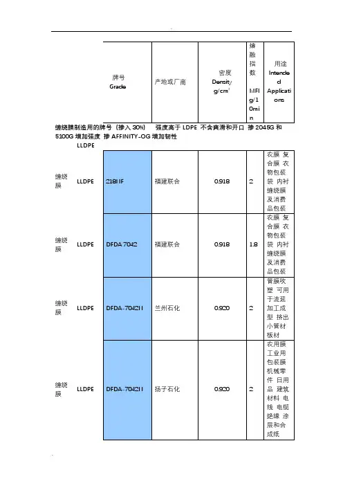
缠绕膜制造用的牌号(掺入30%)强度高于LDPE 不含爽滑和开口掺2045G和5100G增加强度掺AFFINITY-OG增加韧性LLDPE缠绕膜LLDPE缠绕膜LLDPE缠绕膜LLDPE缠绕膜LLDPE 缠绕膜LLDPE缠绕膜LLDPE缠绕膜LLDPE缠绕膜LLDPE缠绕膜LLDPE (6c)薄膜级LLDPE薄膜级LLDPE缠绕膜LLDPE (6c)缠绕膜LLDPE (6c)缠绕膜LLDPE(8C 线性)茂金属茂金属茂金属茂金属茂金属茂金属茂金属茂金属缠绕膜茂金属. 缠绕膜茂金属缠绕膜茂金属缠绕膜茂金属(6c)缠绕膜茂金属缠绕膜茂金属茂金属缠绕茂金属膜茂金属茂金属茂金属茂金属茂金属茂金属茂金属超低密度聚乙烯超低密度聚乙烯超低密度聚乙烯POE弹性体PE弹性体体PE弹性体PP弹性体弹性体弹性体薄膜级LLDPE 薄膜级LLDPE薄膜级LLDPE 薄膜级LLDPE 薄膜级LLDPE 薄膜级LLDPE薄膜级LLDPE 薄膜LLDPE.级薄膜LLDPE级薄膜LLDPE级薄膜LLDPE级薄膜级LLDPE薄膜级LLDPE薄膜级LLDPE 薄膜级LLDPE薄膜级LLDPE薄膜级LLDPE 薄膜级LLDPE薄膜级LLDPE 薄膜级LLDPE薄膜级LLDPE薄膜级LLDPE薄膜级LLDPE 缠绕膜LLDPE缠绕膜LLDPE缠绕膜LLDPE缠绕膜LLDPE薄膜级LLDPE 薄膜级LLDPE薄膜级LLDPE 薄膜级LLDPE 薄膜级LLDPE 薄膜级LLDPE 薄膜级LLDPE薄膜级LLDPE 薄膜级LLDPE薄膜级LLDPE薄膜级LLDPE 薄膜级LLDPE薄膜LLDPE 级薄膜LLDPE 级薄膜LLDPE级薄膜LLDPE 级薄膜LLDPE 级薄膜LLDPE 级薄膜LLDPE 级薄膜LLDPE 级薄膜级LLDPE薄膜级LLDPE薄膜级LLDPE薄膜级LLDPE 薄膜LLDPE级薄膜级LLDPE薄膜级LLDPE薄膜级LLDPE 1820S1 印尼薄膜级LLDPE 201XV 福建联合薄膜级LLDPE 7087科威特EQUATE1薄膜级LLDPE 新加坡注塑级LLDPE注塑级LLDPE注塑LLDPE.级注塑LLDPE级注塑LLDPE级注塑LLDPE级注塑LLDPE级注塑LLDPE级. 注塑级LLDPE注塑级LLDPE高压花料挤出涂覆级LDPE注塑级LDPELDPE 注塑LDPE.级LDPE 注塑级LDPELDPELDPELDPE高压涂覆挤出级LDPE涂覆级LDPE涂覆LDPE.级涂覆级 LDPE注塑级LDPE挤出级LDPE挤出级 LDPE挤出级 LDPELDPE高压薄膜LDPELDPE.LDPELDPE高压重包装注塑级LDPELDPE LDPE LDPE薄膜级LDPE薄膜级LDPE薄膜级LDPE薄膜级LDPE. 薄膜级LDPE薄膜级LDPE薄膜级LDPE薄膜级LDPE薄膜级LDPE薄膜级LDPE薄膜级LDPE薄膜级LDPE薄膜级LDPE薄膜级LDPE 薄膜级LDPE薄膜级LDPE薄膜级LDPE薄膜级LDPE薄膜级LDPE薄膜级LDPE 薄膜级LDPE薄膜级LDPE薄膜级LDPE薄膜级LDPE薄膜级LDPE薄膜级LDPE薄膜级LDPE薄膜级LDPE薄膜级LDPE薄膜级LDPE薄膜级LDPE薄膜级LDPE薄膜LDPE 级薄膜LDPE 级薄膜LDPE 级薄膜LDPE 级薄膜LDPE.级薄膜LDPE级薄膜LDPE级薄膜LDPE级薄膜LDPE. 级注塑级LDPE注塑级LDPE注塑级LDPE 注塑级LDPE注塑级LDPE注塑级LDPE注塑级LDPE注塑级LDPE注塑级LDPE涂覆级LDPE涂覆级LDPE涂覆级LDPE涂覆级LDPE涂覆级LDPE涂覆级LDPE 涂覆级LDPE涂覆级LDPE涂覆级LDPE 7008 美国陶氏薄膜级HDPE薄膜级HDPE薄膜级HDPE薄膜级HDPE薄膜级HDPE薄膜级HDPE薄膜级HDPE薄膜级HDPE薄膜级HDPE薄膜级HDPE薄膜级HDPE薄膜级HDPE薄膜级HDPE薄膜级HDPE薄膜级HDPE 薄膜级HDPE薄膜级HDPE 薄膜级HDPE薄膜级HDPE薄膜级HDPE薄膜级HDPE 薄膜级HDPE 薄膜级HDPE薄膜级HDPE注塑级HDPE 低压聚乙烯MI:5属于低熔指MI:10属于中熔指MI:20属于高熔指注塑级HDPE注塑级HDPE注塑级HDPE注塑级HDPE注塑级HDPE注塑级HDPE注塑级HDPE注塑级HDPE注塑级HDPE注塑级HDPE注塑级HDPE注塑级HDPE注塑级HDPE 注塑级HDPE注塑级HDPE注塑级HDPE注塑级HDPE注塑级HDPE 注塑级HDPE。
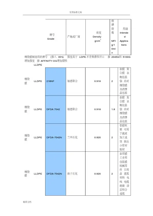
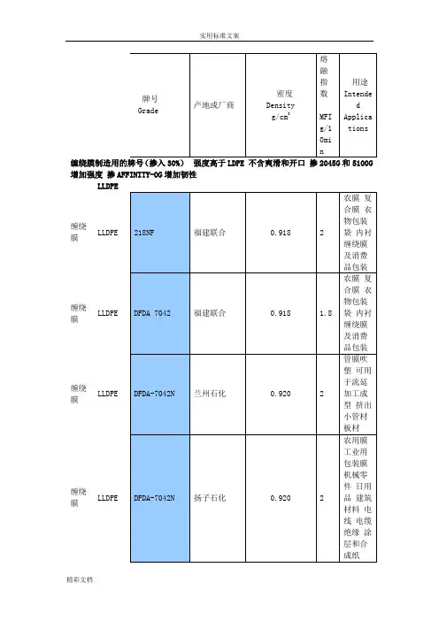
增加强度掺AFFINITY-OG增加韧性LLDPE缠绕LLDPE膜缠绕LLDPE膜缠绕LLDPE膜缠绕LLDPE膜缠绕膜LLDPE缠绕膜LLDPE缠绕膜LLDPE缠绕膜LLDPE缠绕膜LLDPE (6c)薄膜级LLDPE薄膜级LLDPE缠绕膜LLDPE (6c)缠绕膜LLDPE (6c)缠绕膜LLDPE( 8C线性)茂金属茂金属茂金属茂金属茂金属茂金属茂金属茂金属缠绕茂金属膜缠绕茂金属膜缠绕茂金属膜缠绕膜茂金属(6c)缠绕膜茂金属缠绕膜茂金属茂金属缠绕膜茂金属茂金属茂金属茂金属茂金属茂金属茂金属茂金属烯超低密度聚乙烯超低密度聚乙烯POE弹性体PE弹性体PE弹性体PE弹性体PP弹性体弹性体弹性体薄膜级LLDPE薄膜级LLDPE薄膜级LLDPE 薄膜级LLDPE 薄膜级LLDPE 薄膜级LLDPE薄膜级LLDPE薄膜级LLDPE薄膜级LLDPE薄膜级LLDPE薄膜级LLDPE薄膜级LLDPE薄膜级LLDPE薄膜级LLDPE薄膜级LLDPE薄膜级LLDPE薄膜级LLDPE 薄膜级LLDPE薄膜级LLDPE薄膜级LLDPE薄膜级LLDPE薄膜级LLDPE薄膜级LLDPE缠绕膜LLDPE缠绕膜LLDPE缠绕膜LLDPE缠绕膜LLDPE薄膜级LLDPE薄膜级LLDPE薄膜级LLDPE 薄膜级LLDPE薄膜级LLDPE薄膜级LLDPE 薄膜级LLDPE薄膜级LLDPE薄膜级LLDPE薄膜级LLDPE薄膜级LLDPE薄膜级LLDPE薄膜级LLDPE薄膜级LLDPE薄膜级LLDPE薄膜级LLDPE薄膜级LLDPE薄膜级LLDPE薄膜级LLDPE薄膜级LLDPE薄膜级LLDPE 薄膜级LLDPE薄膜级LLDPE薄膜级LLDPE 薄膜级LLDPE 薄膜级 LLDPE薄膜级 LLDPE 薄膜级 LLDPE 1820S1 印尼 薄膜级 LLDPE 201XV 福建联合 薄膜级 LLDPE 7087 科威特EQUATE 1 薄膜级 LLDPE 新加坡注塑级 LLDPE 注塑级 LLDPE 注塑LLDPE级注塑级LLDPE 注塑级 LLDPE 注塑级LLDPE注塑级LLDPE注塑级LLDPE 注塑级LLDPE 注塑级LLDPE 高压花料 挤出涂覆级LDPE 注塑级LDPELDPE注塑LDPE 级LDPE注塑LDPE 级LDPELDPELDPE 高压涂覆挤出LDPE 级涂覆LDPE 级涂覆LDPE 级涂覆LDPE 级注塑LDPE 级挤出LDPE 级挤出LDPE 级挤出级LDPELDPE高压薄膜LDPELDPELDPELDPE 高压重包装注塑级LDPELDPELDPELDPE 薄膜级LDPE薄膜级LDPE薄膜级LDPE薄膜级LDPE薄膜级LDPE薄膜级LDPE薄膜级LDPE薄膜级LDPE薄膜级LDPE薄膜级LDPE薄膜级LDPE薄膜级LDPE薄膜级LDPE薄膜级LDPE 薄膜级LDPE薄膜级LDPE薄膜级LDPE薄膜级LDPE薄膜级LDPE薄膜级LDPE薄膜级LDPE薄膜级LDPE薄膜级LDPE薄膜级LDPE薄膜级LDPE薄膜级LDPE薄膜级LDPE薄膜级LDPE薄膜级LDPE薄膜级LDPE薄膜级LDPE薄膜级LDPE薄膜级LDPE薄膜级LDPE薄膜级LDPE薄膜级LDPE 薄膜级LDPE 薄膜级LDPE薄膜级LDPE薄膜级LDPE薄膜级LDPE注塑级LDPE注塑级LDPE注塑级LDPE 注塑级LDPE注塑级LDPE注塑级LDPE注塑级LDPE注塑级LDPE注塑级LDPE涂覆级LDPE涂覆级LDPE涂覆级LDPE涂覆级LDPE 涂覆级LDPE涂覆级LDPE 涂覆级LDPE 涂覆级LDPE 涂覆级 LDPE 7008 美国陶氏 薄膜级 HDPE 薄膜HDPE级薄膜HDPE 级薄膜HDPE 级薄膜HDPE 级薄膜HDPE 级薄膜HDPE 级薄膜HDPE 级薄膜HDPE 级薄膜HDPE 级薄膜HDPE 级薄膜HDPE 级薄膜HDPE 级薄膜HDPE 级薄膜HDPE 级薄膜HDPE 级薄膜HDPE 级薄膜HDPE级 薄膜级HDPE薄膜级 HDPE 薄膜级 HDPE 薄膜级HDPE薄膜级HDPE 薄膜级HDPE注塑级HDPE 低压聚乙烯 MI :5属于低熔指 MI :10属于中熔指 MI :20属于高熔指注塑级HDPE 注塑级 HDPE 注塑级 HDPE 注塑HDPE级注塑HDPE 级注塑HDPE 级注塑HDPE 级注塑HDPE 级注塑HDPE 级注塑HDPE 级注塑HDPE 级注塑HDPE 级注塑级HDPE 注塑级HDPE注塑级HDPE注塑级HDPE注塑级HDPE注塑级HDPE注塑级HDPE注塑级HDPE注塑级HDPE注塑级HDPE注塑级HDPE注塑级HDPE注塑级HDPE注塑级HDPE注塑级HDPE注塑级HDPE注塑级HDPE注塑级HDPE注塑级HDPE注塑级HDPE注塑级HDPE注塑级HDPE注塑级HDPE 注塑级HDPE注塑级HDPE注塑级HDPE注塑级HDPE拉丝级HDPE拉丝级HDPE拉丝级HDPE拉丝级HDPE拉丝级HDPE拉丝级HDPE拉丝级HDPE拉丝级HDPE拉丝级HDPE 拉丝级HDPE拉丝级HDPE拉丝级HDPE拉丝级HDPE拉丝级HDPE拉丝级HDPE中空级HDPE中空级HDPE中空级HDPE中空级HDPE中空级HDPE中空级HDPE中空级HDPE 中空HDPE级中空HDPE 级中空HDPE 级中空HDPE 级中空HDPE 级中空HDPE 级中空级HDPE中空级HDPE中空级HDPE中空级HDPE中空级HDPE中空级HDPE中空级HDPE中空级HDPE中空级HDPE中空级HDPE中空级HDPE中空级HDPE 中空级HDPE中空级HDPE 拉丝级PP拉丝级PP拉丝级 PP拉丝级PP拉丝级PP 拉丝级 PP 拉丝级 PP 拉丝级PP注塑级PP注塑级PP注塑级PP注塑级PP 注塑级PP 注塑级 PP 注塑级PP 注塑级PP。
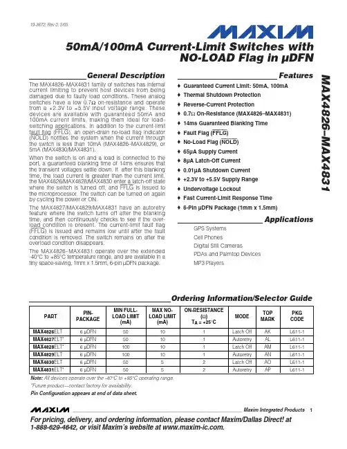
General DescriptionThe MAX4826–MAX4831 family of switches has internal current limiting to prevent host devices from being damaged due to faulty load conditions. These analog switches have a low 0.7Ωon-resistance and operate from a +2.3V to +5.5V input voltage range. These devices are available with guaranteed 50mA and 100mA current limits, making them ideal for load-switching applications. In addition to the current-limit fault flag (FFLG ), an open-drain no-load flag indicator (NOLD) notifies the system when the current through the switch is less than 10mA (MAX4826–MAX4829), or 5mA (MAX4830/MAX4831).When the switch is on and a load is connected to the port, a guaranteed blanking time of 14ms ensures that the transient voltages settle down. If, after this blanking time, the load current is greater than the current limit,the MAX4826/MAX4828/MAX4830 enter a latch-off state where the switch is turned off, and FFLG is issued to the microprocessor. The switch can be turned on again by cycling the power or ON.The MAX4827/MAX4829/MAX4831 have an autoretry feature where the switch turns off after the blanking time, and then continuously checks to see if the over-load condition is present. The current-limit fault flag (FFLG ) is issued and remains low until after the fault condition is removed. The switch remains on after the overload condition disappears.The MAX4826–MAX4831 operate over the extended -40°C to +85°C temperature range, and are available in a tiny space-saving, 1mm x 1.5mm, 6-pin µDFN package.Features♦Guaranteed Current Limit: 50mA, 100mA♦Thermal Shutdown Protection ♦Reverse-Current Protection♦0.7ΩOn-Resistance (MAX4826–MAX4831)♦14ms Guaranteed Blanking Time ♦Fault Flag (FFLG )♦No-Load Flag (NOLD )♦65µA Supply Current ♦8µA Latch-Off Current ♦0.01µA Shutdown Current ♦+2.3V to +5.5V Supply Range ♦Undervoltage Lockout♦Fast Current-Limit Response Time ♦6-Pin µDFN Package (1mm x 1.5mm)ApplicationsGPS Systems Cell Phones Digital Still Cameras PDAs and Palmtop Devices MP3 PlayersMAX4826–MAX483150mA/100mA Current-Limit Switches withNO-LOAD Flag in µDFN________________________________________________________________Maxim Integrated Products1Ordering Information/Selector Guide19-3672; Rev 0; 5/05For pricing, delivery, and ordering information,please contact Maxim/Dallas Direct!at 1-888-629-4642, or visit Maxim’s website at .*Future product—contact factory for availability.Pin Configuration appears at end of data sheet.M A X 4826–M A X 483150mA/100mA Current-Limit Switches with NO-LOAD Flag in µDFN 2_______________________________________________________________________________________ABSOLUTE MAXIMUM RATINGSStresses beyond those listed under “Absolute Maximum Ratings” may cause permanent damage to the device. These are stress ratings only, and functional operation of the device at these or any other conditions beyond those indicated in the operational sections of the specifications is not implied. Exposure to absolute maximum rating conditions for extended periods may affect device reliability.IN, ON, FFLG , NOLD , OUT to GND .........................-0.3V to +6V OUT Short Circuit to GND.................................Internally Limited Continuous Power Dissipation (T A = +70°C)6-Pin µDFN (derate 2.1mW/C above +70°C)...............168mW Operating Temperature Range ...........................-40°C to +85°CJunction Temperature......................................................+150°C Storage Temperature Range.............................-65°C to +150°C Lead Temperature (soldering, 10s).................................+300°CELECTRICAL CHARACTERISTICS(V IN = +2.3V to +5.5V, T A = -40°C to +85°C, unless otherwise noted. Typical values are at V IN = +3.3V, T A = +25°C.) (Note 1)MAX4826–MAX483150mA/100mA Current-Limit Switches withNO-LOAD Flag in µDFN_______________________________________________________________________________________3ELECTRICAL CHARACTERISTICS (continued)(V IN = +2.3V to +5.5V, T A = -40°C to +85°C, unless otherwise noted. Typical values are at V IN = +3.3V, T A = +25°C.) (Note 1)Note 2:Latch-off current does not include the current flowing into FFLG and NOLD .Note 3:Turn-on time is defined as the time taken for the current through the switch to go from 0mA to full load. Turn-off time isdefined as the time taken for the current through the switch to go from full load to 0mA.Note 4:Retry time is typically 14x the blanking time.Typical Operating Characteristics(V IN = +3.3V, T A = +25°C, unless otherwise noted.)QUIESCENT SUPPLY CURRENTvs. SUPPLY VOLTAGESUPPLY VOLTAGE (V)S U P P L Y C U R R E N T (µA )5.14.73.9 4.33.1 3.52.710203040506070809002.3 5.5TEMPERATURE (°C)603510-15-4085QUIESCENT SUPPLY CURRENTvs. TEMPERATURES U P P L Y C U R R E N T (µA )10203040506070809001234567891011121314150TEMPERATURE (°C)603510-15-4085LATCH-OFF CURRENT vs. TEMPERATUREL A T C H -O F F C U R R E N T (µA )M A X 4826–M A X 483150mA/100mA Current-Limit Switches with NO-LOAD Flag in µDFN 4_______________________________________________________________________________________Typical Operating Characteristics (continued)(V IN = +3.3V, T A = +25°C, unless otherwise noted.)SHUTDOWN SUPPLY CURRENTvs. TEMPERATURETEMPERATURE (°C)S H U T D O W N S U P P L Y C U R R E N T (n A )0.0010.010.11100.0001603510-15-4085SHUTDOWN LEAKAGE CURRENTvs. TEMPERATURETEMPERATURE (°C)S H U T D O W N L E A K A G E C U R R E N T (n A )0.0010.010.11100.0001603510-15-4085SHUTDOWN REVERSE LEAKAGE CURRENTvs. TEMPERATURETEMPERATURE (°C)R E V E R S E L E A K A G E C U R R E N T (n A )0.0010.010.11100.0001603510-15-4085LATCH-OFF-LEAKAGE CURRENTvs. TEMPERATURETEMPERATURE (°C)L A T C H -O F F -L E A K A G E C U R R E N T (n A )0.0010.010.11100.0001603510-15-4085TEMPERATURE (°C)603510-15-4085NORMALIZED ON-RESISTANCEvs. TEMPERATUREN O R M A L I Z E D R O N0.20.40.60.81.01.21.4010050200150********.60.9 1.20.3 1.5 1.8 2.1 2.4 2.7 3.0 3.3OUTPUT CURRENT vs. OUTPUT VOLTAGEV IN - V OUT (V)O U T P U T C U R R E N T (m A )SWITCH TURN-ON/OFF TIMESvs. TEMPERATURETEMPERATURE (°C)T U R N -O N /O F F T I M E S (µs )0.010.11101000.001603510-15-4085FLAG-BLANKING TIMEOUT vs. TEMPERATUREF L AG -B L A N K I N G T I M E (m s )15202530354010M A X 4826 t o c 11TEMPERATURE (°C)603510-15-4085MAX4826–MAX483150mA/100mA Current-Limit Switches withNO-LOAD Flag in µDFN_______________________________________________________________________________________5CURRENT-LIMIT RESPONSE40µs/div V ON = 3.3V V OUT = GND C IN = 1µF C OUT = 1µFV IN 2V/div V ON 2V/divI OUT100mA/div CURRENT-LIMIT RESPONSE (OUT SHORTED TO GND)MAX4826 toc1440µs/divV IN 2V/div V OUT 2V/divI OUT 2A/divCURRENT-LIMIT RESPONSEMAX4826 toc1320µs/divV ON = 3.3V V OUT = GND C IN = 1µF C OUT = 1µFV IN = V ON 1V/divI OUT100mA/divSWITCH TURN-ON-TIME RESPONSE100µs/divV IN = 3.3V I LOAD = 10mAV ON 2V/divI OUT100mA/divTypical Operating Characteristics (continued)(V IN = +3.3V, T A = +25°C, unless otherwise noted.)SWITCH TURN-OFF-TIME RESPONSE100ns/divV ON 2V/divI OUT10mA/divV IN = 3.3V I LOAD = 10mAFLAG-BLANKING RESPONSEMAX4826 toc174ms/divV IN 2V/divV ON 2V/divI OUT100mA/divFFLG 2V/divM A X 4826–M A X 4831Detailed DescriptionThe MAX4826–MAX4831 are forward-/reverse-current-limited switches that operate from a +2.3V to +5.5V input voltage range and guarantee a 50mA and 100mA minimum current-limit threshold for different options.The voltage drop across an internal sense resistor is compared to two reference voltages to indicate a for-ward- or reverse-current-limit fault. When the load cur-rent exceeds the preset current limit for greater than the fault-blanking time, the switch opens.The MAX4827/MAX4829/MAX4831 have an autoretry function that turns on the switch again after an internal retry time expires. If the faulty load condition is still pre-sent after the blanking time, the switch turns off again and the cycle is repeated. If the faulty load condition is not present, the switch remains on.The MAX4826/MAX4828/MAX4830 do not have the autoretry option, and the switch remains in latch-off mode until ON or the input power is cycled from high to low and then high again.The undervoltage lockout (UVLO) circuit prevents erro-neous switch operation when the input voltage goes too low during startup conditions.The MAX4826–MAX4831 limit the reverse current (V OUT to V IN ) from exceeding the maximum I REV value. The switch is shut off and FFLG is asserted if the reverse-current-limit condition persists for more than the blank-ing time. This feature prevents excessive reverse cur-rents from flowing through the device.Switch-On/Off ControlToggle ON high to enable the current-limited switches.The switches are continuously on only if V IN exceeds the UVLO threshold (typically 2V) and there is no fault.When a forward-/reverse-current fault is present or the die exceeds the thermal-shutdown temperature of +150°C, OUT is internally disconnected from IN, and the supply current decreases to 8µA (latch off). The switch is now operating in one of its off states. The switch off state also occurs when driving ON low, thus reducing the supply current (shutdown) to 0.01µA.Table 1 illustrates the ON/OFF state of the MAX4826–MAX4831 current-limit switches.50mA/100mA Current-Limit Switches with NO-LOAD Flag in µDFNFFLG IndicatorThe MAX4826–MAX4831 feature a current-limit fault output, FFLG . Whenever a current-limit fault is activat-ed, FFLG goes low and the switch turns off. FFLG is an open-drain output transistor and requires an external pullup resistor from FFLG to IN. During shutdown (ON is low), the pulldown on the FFLG output is released to limit power dissipation. FFLG goes low when any of the following conditions occur:• The die temperature exceeds the thermal shut-down temperature limit of +150°C.• The device is in current limit for more than the fault-blanking period.• V IN is below the UVLO threshold.NOLD IndicatorThe MAX4826–MAX4831 feature a no-load flag output,NOLD (Figure 1). This output is pulled low every time the current coming out of the switch is less than 10mA (MAX4826–MAX4829), or 5mA (MAX4830/MAX4831).NOLD is an open-drain output transistor and requires an external pullup resistor from NOLD to a supply up to +5.5V. Current through the switch is intended to be positive (from IN to OUT), and for currents that are large in magnitude but negative in sign (OUT to IN),NOLD asserts low. For options with the autoretry fea-ture (MAX4827/MAX4829/MAX4831), the NOLD output is high impedance during the t RETRY period when a for-ward-current-limit condition is present. However, NOLD is pulled low if a reverse current-limit condition is pre-sent during the t RETRY period. A constant time filter is present at the output of NOLD that gives a 60µs delay when a no-load condition is asserted. Deassertion of NOLD is not delayed. During shutdown (ON is low), the pulldown on NOLD is released to limit power dissipation.Autorety (MAX4827/MAX4829/MAX4831)When the forward- or reverse-current-limit threshold is exceeded, the t BLANK timer begins counting (Figure 2).The timer resets if the overcurrent condition disappears before t BLANK has elapsed. A retry time delay, t RETRY ,MAX4826–MAX483150mA/100mA Current-Limit Switches withNO-LOAD Flag in µDFN_______________________________________________________________________________________7Figure 3. MAX4826/MAX4828/MAX4830 Latch-Off Fault BlankingFigure 2. MAX4827/MAX4829/MAX4831 Autoretry Fault Blanking DiagramFigure 1. MAX4826–MAX4831 No-Load Flag ResponseM A X 4826–M A X 4831is started immediately after t BLANK has elapsed, and during that time the switch is latched off. At the end of t RETRY , the switch is turned on again. If the fault still exists, the cycle is repeated. If the fault has been removed, the switch stays on.The autoretry feature saves system power in the case of an overcurrent or short-circuit condition. During t BLANK ,when the switch is on, the supply current is at the cur-rent limit. During t RETRY , when the switch is off, no cur-rent flows through the switch. Instead of observing the full load current, the switch sees the equivalent load current, multiplied by the duty cycle or I SUPPLY = I LOAD x t BLANK / (t BLANK + t RETRY ). With a typical t BLANK =37ms and typical t RETRY = 518ms, the duty cycle is 6%which results in a 94% power savings, as opposed to the switch being on the entire time. The duty cycle is consistent across the process and devices.Latch Off (MAX4826/MAX4828/MAX4830)When the forward- or reverse-current-limit threshold is exceeded, the t BLANK timer begins counting. The timer resets if the overcurrent condition disappears before t BLANK has elapsed. The switch is shut off if the over-current condition continues up to the end of the blank-ing time. Reset the switch by either toggling ON (Figure 3a), or cycling the input voltage below UVLO, typically 2V (Figure 3b).Fault BlankingThe MAX4826–MAX4831 feature 14ms (min) fault blank-ing. Fault blanking allows current-limit faults, including momentary short-circuit faults that occur when hot swap-ping a capacitive load. Fault blanking also ensures that no fault is issued during power-up. When a load transient causes the device to enter the current limit, an internal counter starts. If the load-transient fault persists beyond the fault-blanking timeout, FFLG asserts low. Load-tran-sient faults less than t BLANK do not cause FFLG asser-tion. Only current-limit faults are blanked.A thermal fault and input voltage drops below the UVLO threshold cause FFLG to assert immediately. These faults do not wait for the blanking time.Thermal ShutdownThe MAX4826–MAX4831 have a thermal-shutdown fea-ture to protect the devices from overheating. The switch turns off and FFLG goes low immediately (no fault blanking) when the junction temperature exceeds +150°C. The switches with the autoretry feature turn back on when the device temperature drops approxi-mately 15°C. The switches with the latch-off feature require ON cycling.Applications InformationInput CapacitorTo limit the input voltage drop during momentary output short-circuit conditions, connect a capacitor from IN to GND. A 0.1µF ceramic capacitor is adequate for most applications; however, higher capacitor values further reduce the voltage drop at the input and are recom-mended for lower voltage applications.Output CapacitanceConnect a 0.1µF capacitor from OUT to GND. This capacitor helps prevent inductive parasitics from pulling OUT negative during turn-off, thus preventing the MAX4826–MAX4831 from tripping erroneously. If the load capacitance is too large, current may not have enough time to charge the capacitance, and the device assumes that there is a faulty load condition. The maxi-mum capacitive load value that can be driven from OUT is obtained by the following formula:Layout and Thermal DissipationTo optimize the switch response time to output short-circuit conditions, it is very important to keep all traces as short as possible to reduce the effect of undesirable parasitic inductance. Place input and output capacitors as close as possible to the device (no more than 5mm).IN and OUT pins must be connected with short traces to the power bus.During normal operation, the power dissipation is small and the package temperature change is minimal. If the output is continuously shorted to ground at the maxi-mum supply voltage, the operation of the switches with the autoretry option does not cause problems because the total power dissipated during the short is scaled by the duty cycle:where,V IN_MAX = 5.5V, I OUT_MAX = 240mA, t BLANK = 37ms,and t RETRY = 518ms.Attention must be given to the MAX4826/MAX4828/MAX4830 where the latch-off condition must be manually reset by toggling ON from high to low. If the latch-off time duration is not sufficiently high, it is possible for the device to reach the thermal shutdown threshold andnever be able to turn the device on until it cools down.50mA/100mA Current-Limit Switches with NO-LOAD Flag in µDFN 8_______________________________________________________________________________________MAX4826–MAX483150mA/100mA Current-Limit Switches withNO-LOAD Flag in µDFNChip InformationTRANSISTOR COUNT: 1175PROCESS: BiCMOSPin ConfigurationTypical Operating CircuitFunctional DiagramM A X 4826–M A X 483150mA/100mA Current-Limit Switches with NO-LOAD Flag in µDFN Maxim cannot assume responsibility for use of any circuitry other than circuitry entirely embodied in a Maxim product. No circuit patent licenses are implied. Maxim reserves the right to change the circuitry and specifications without notice at any time.10____________________Maxim Integrated Products, 120 San Gabriel Drive, Sunnyvale, CA 94086 408-737-7600©2005 Maxim Integrated ProductsPrinted USAis a registered trademark of Maxim Integrated Products, Inc.MAX4826–MAX4831Package Information(The package drawing(s) in this data sheet may not reflect the most current specifications. For the latest package outline information,go to /packages .)6L U D F N .E P S。