TMS320C6455的DDR2电路的信号完整性设计
- 格式:pdf
- 大小:733.01 KB
- 文档页数:4
1Prerequisites PreliminaryApplication ReportSPRAAA8A–August2006Implementing Serial Rapid I/O PCB Layout on aTMS320C6455Hardware Design Todd Hiers DSP Hardware ApplicationsThis application report contains implementation instructions for the Serial Rapid I/O(SRIO)interface on the TMS320C6455DSP device.The approach to specifyinginterface timing and physical requirements for the SRIO interface is quite different thanprevious approaches for other interfaces.Serial Rapid I/O is an industry-standard high-speed switched-packet interconnect.Physical layer data transmission utilizes analog serializer/deserializers(serdes)to feedlow-output-swing differential CML buffers.Proper printed circuit board(PCB)design forthis interface resembles analog or RF design,and is very different than traditionalparallel digital bus design.Due to this analog nature of SRIO,it is not possible to specify the interface in atraditional DSP digital interface manner.Furthermore,it is undesirable to specify theinterface in terms of the raw physical requirements laid out by the SRIO specification.Understanding the SRIO specification and producing a compliant PCB based on theexplicit and implicit requirements there demands significant time,experience,andexpensive tools.For the TMS320C6455SRIO interface,the approach is to reduce the specification to aset of easy-to-follow PCB routing rules.TI has performed the simulation and systemdesign work to ensure SRIO interface requirements are met.This document describesthe content of this SRIO implementation.Contents1Prerequisites (1)2TMS320C6455Supported Serial RapidIO Devices (2)3Description of the Serial Rapid I/O Hardware Design Files (2)4PCB Routing Rules (2)5Device Settings (7)6References (10)The goal of the C6455collateral is to make system implementation easier for the customer by providing the system solution.For this Serial RapidIO(SRIO)interface,it is not assumed that the system designer is familiar with SRIO,serializer-deserializer(SERDES)technology,or RF/Microwave PCB design.However, it is still expected that the PCB design work be supervised by a knowledgeable high speed digital PCB designer and an assumption is made that the PCB designer is using established high speed design rules.SPRAAA8A–August2006Implementing Serial Rapid I/O PCB Layout on a TMS320C6455Hardware Design1 Submit Documentation Feedback2TMS320C6455Supported Serial RapidIO Devices3Description of the Serial Rapid I/O Hardware Design Files4PCB Routing Rules 4.1Minimum PCB Stackup4.2General Trace/Space and Via SizesPreliminaryTMS320C6455Supported Serial RapidIO DevicesRapidIO is an industry-standard high-speed switched-packet interconnect.The RapidIO specification allows a device to connect to any other device,so long as the two devices conform to a commonphysical-layer specification.TI DSPs support connecting to any Serial RapidIO device that complies with the Serial RapidIO specification revision 1.2or later.The SRIO Hardware Design files included with this report are described inTable 1.Table 1.SRIO Hardware Design FilesThe minimum PCB stackup for routing the TMS320C6455is a six-layer stackup as described in Table 2.Table 2.Minimum PCB StackupLayer Type Description 1Signal Top Routing 2Plane Ground 3Plane Split Power 4Signal Internal Routing5Plane Ground 6SignalBottom RoutingAdditional layers may be added as needed.All layers with SRIO traces must be able to achieve 100ohms differential impedance.Note:The provided sample board file shows a twelve-layer stackup,but not all of these layers are necessary to use the SRIO interface.The key concern for RapidIO signal traces is to achieve 100Ohm differential impedance.This differential impedance is impacted by trace width,trace spacing,distance between planes,and dielectric material.Verify with a proper PCB manufacturing tool that the trace geometry for all SRIO traces results in exactly 100Ohms differential impedance traces.Of secondary concern is the insertion loss caused by the traces.Due to the skin effect,wider traces will have lower losses than narrower ones.Therefore,longer SRIO runs should use wider traces for lower yers in the stackup that are set to 100Ohm differential impedance with wider traces may be less desirable for routing other signals.Table 3shows recommendations for minimum trace width by SRIO signal run lengthImplementing Serial Rapid I/O PCB Layout on a TMS320C6455Hardware Design2SPRAAA8A–August 2006Submit Documentation Feedback4.3Serial RapidIO Interface Routing Requirements4.3.1Receiver EndPreliminaryPCB Routing RulesTable 3.Minimum Trace WidthSignal Run Length,up to Minimum trace width 10in /25cm 4mil /.1mm 20in /50cm 6mil /.15mm 30in /75cm8mil /.2mmThe C6455sample PCB is routed using 4mil traces and 4mil minimum trace spacing.100Ohmsdifferential impedance is achieved with 4mil traces and 10mil spaces on the Top and Bottom layers,and 4mil traces with 5mil spaces on internal layers.Escape and general SRIO routing vias have 8mil holes with 18mil pads.Micro and/or blind/buried vias are neither required nor prohibited.The PCB BGA padC6455by the Flip Chip Ball Grid Array Package Reference Guide available at The C6455is a 0.8mm ball pitch part and should follow the 0.8The PCB for the SRIO link partner device should follow its manufacturer's guidelines.The approach used in this reference design for specifying suitable RapidIO routing breaks the physical connection down into three component pieces:receiver end,transmitter end,and interconnect.The receiver and transmitter end are the pieces closest to the packages of the connected devices.The receiver end goes from the BGA pads to the capacitors.The transmitter end is simply the BGA escape paths for the differential pairs.Those two pieces of the reference layout are designed to be copied exactly into the target board.The interconnect joins the receiver and transmitter ends,and it is not intended to be copied directly,as board placements will vary from the sample.Figure 1below shows the connection on the receiver end.The trace from the BGA pad to the capacitor be on the top layer.On the other side of the capacitor,it is recommended to via to another layer.The BGA breakout should be implemented exactly as shown.The trace widths and separation should be altered based on the board stackup to meet the 100Ωdifferential impedance requirement.Also,traces may be necked down to escape the BGA,if necessary.An 0402or smaller size,0.1µf capacitor is recommended for AC coupling of the data lines.SPRAAA8A–August 2006Implementing Serial Rapid I/O PCB Layout on a TMS320C6455Hardware Design 3Submit Documentation FeedbackPreliminary PCB Routing RulesFigure1.Receiver END BGA Breakout4.3.2Transmitter EndFigure2below shows the connection on the transmitter end.This trace may be on any signal layer the top.Internal layers are recommended for their superior shielding characteristics.The BGA breakout should be implemented exactly as shown.The trace widths and separation should be altered based on the board stackup to meet the100Ωdifferential impedance requirement.Also,traces may be necked down to escape the BGA,if necessary.4Implementing Serial Rapid I/O PCB Layout on a TMS320C6455Hardware Design SPRAAA8A–August2006Submit Documentation Feedback4.3.3Interconnect4.3.4Length MatchingPreliminaryPCB Routing RulesFigure 2.Transmitter End BGA BreakoutThe geometry of the traces to link the transmitter and receiver ends is determined by the placement in the target system.Therefore,it is not possible to specify an exact layout for the interconnect.Instead,the trace may be placed as required,so long as it meets the following requirements:•Edge-coupled,matched-length (±50mils)differential pair •No stubs•No more than 30inches (75cm)pin-to-pin,for 8-mil (.2mm)wide traces over FR4material •100Ωdifferential impedance•No more than 3sets of vias (not including via for BGA breakout on transmit end)•Other signals are separated by at least 2x the differential spacing •Internal layers are strongly preferred.Avoid top and bottom layers•If connectors are used,they must be of a suitable 100ohm differential-impedance,high-speed type,and count as 1”of trace for each connector pair•If cabling is used,it must be of a suitable controlled-impedance type (100ohm differential or 50ohm single ended),and counts as 1"of trace for each 1'of cable.•If a mid bus probe is used,it must follow both TI’s and the probe manufacturer’s guidelines,and counts as 2”of traceIf the SRIO peripheral will be used in 1x mode,then there is no lane-to-lane length matching requirement.If the SRIO peripheral will be used in 4x mode,then:•All TX lanes connected to a device must all be +/-5inches (12.5cm)in length from each other •All RX lanes connected to a device must all be +/-5inches (12.5cm)in length from each other •There is no requirement that the TX lengths match the RX lengthsSPRAAA8A–August 2006Implementing Serial Rapid I/O PCB Layout on a TMS320C6455Hardware Design5Submit Documentation Feedback4.3.5Mid Bus Probe (Optional)4.3.6Connectors (Optional)4.3.7Cabling (Optional)PreliminaryPCB Routing RulesA mid bus probe can be used to observe traffic flowing down a link.Because the probe requires a special attachment point,it can degrade signal quality.The following rules must be observed to include a mid bus probe:•Follow the Probe manufacturer’s guidelines for probe pads and layout•If the stubs can be kept under 250mils (6.35mm)then connecting the probe lands as stubs to the transmission line is acceptable•If the stubs cannot be kept under 250mils (6.35mm)then the probe lands should be connected in-line with the rest of the transmission lineAny connectors used must be controlled impedance (50Ohm single ended or 100Ohm differential)and suitable for microwave transmissions.Suitable connectors are typically categorized as “backplane”type connectors.The connectors should have less than 1dB insertion loss below 6GHz.Some suggested connectors are:•CN074–AMC Connector •Tyco Z-DOK•Tyco Z-PAK HM ZdAny cabling used must be controlled impedance (50Ohm single ended or 100Ohm differential)and suitable for microwave transmissions.Recommended cable types are listed below:•50Ohm Coaxial –Commonly used with SMA connectors,4cables required for 1x link,16for 4x link q RG142q RG316q RG178•Infiniband –assembled cables available in 1x and 4x widthsImplementing Serial Rapid I/O PCB Layout on a TMS320C6455Hardware Design6SPRAAA8A–August 2006Submit Documentation Feedback4.4Power SupplyRequirements5Device SettingsPreliminaryDevice SettingsThe power supply and bypassing requirements foras part of the TMS320C6455Design Guide and Comparisons to TMS320TC6416T Figure 3.Power Plane SplitsSome of the SERDES register values should be set based on parameters from the physical PCB.Others are not dependent on the PCB,but are set based on the SRIO electrical specification.The following sections describe the recommended settings for the receivers and transmitters.More these registers can be found in the TMS320C645x Serial Rapid IO (SRIO)User’s Guide SPRAAA8A–August 2006Implementing Serial Rapid I/O PCB Layout on a TMS320C6455Hardware Design 7Submit Documentation Feedback5.1Receive Channel ConfigurationPreliminaryDevice SettingsTable 4lists the recommended settings for receiver channels that can be set in the SERDES Receive Channel Configuration Registers (SERDES_CFGRXn_CNTL).Table 4.SERDES Receive Channel Configuration Register SettingsBits Field Setting Description19:22EQ 0001Fully Adaptive Equalization 18:16CDR000First Order.Sufficient for SRIO clocking scheme(asynchronous with low frequency offset)15:14LOS 00Disabled.Loss of Signal detection not used in SRIO 13:12ALIGN01Comma Alignment.SRIO uses comma alignment during lane initialization10:8TERM 001Common point is 80%ofVDDT.This is the appropriate setting for AC coupled lines 7INVPAIR 0Non-inverted –use when TXP connects to RXP and TXN connects to RXN1Inverted –use when TXP connects to RXN and TXN connects to RXP (1)6:5RATE 00Full –Use for 3.125GHz and 2.5GHz line rates01Half –Use for 1.25GHz line rate4:2BUS-WIDTH 00010-bit.SRIO uses 10-bit character groups.ENRX0Disabled –for unused lanes 1Enabled –for active lanes(1)On inverted pairs,polarity inversion can be done at the receiver end or the transmitter end,but not bothImplementing Serial Rapid I/O PCB Layout on a TMS320C6455Hardware Design8SPRAAA8A–August 2006Submit Documentation Feedback5.2Transmit Channel Configuration PreliminaryDevice SettingsTable5lists the recommended settings for transmitter channels that can be set in the SERDES Transmit Channel Configuration Registers(SERDES_CFGTXn_CNTL).Table5.SERDES Transmit Channel Configuration Register Settings Bits Field Setting Description16ENFTP1Fixed Phase.Required for4xmode.Do not care in1x mode.15:e for lines up to10inches(25cm)e for lines up to14inches(35cm)e for lines up to18inches(45cm)e for lines up to22inches(55cm)e for lines up to26inches(65cm)e for lines up to30inches(75cm) 11:e for lines up to10inches(25cm)e for lines up to20inches(50cm)e for lines up to30inches(75cm) 8CM1Raised Common Mode.Helpfulin preventing signal distortionat SWING amplitudes over750mV 7INVPAIR0Non-inverted–use when TXPconnects to RXP and TXNconnects to RXN1Inverted–use when TXPconnects to RXN and TXNconnects to RXP(1) 6:5RATE00Full–Use for3.125GHz and2.5GHz line rates01Half–Use for1.25GHz linerate4:2BUS WIDTH00010-bit.SRIO uses10-bitcharacter groups.0ENTX0Disabled–for unused lanes1Enabled–for active lanes(1)On inverted pairs,polarity inversion can be done at the receiver end or the transmitter end,but not bothSPRAAA8A–August2006Implementing Serial Rapid I/O PCB Layout on a TMS320C6455Hardware Design9 Submit Documentation Feedback6ReferencesPreliminaryReferencesmay be downloaded from the RapidIO Trade Association’s web site,The TMS320C645x Serial Rapid IO (SRIO)User’s Guide explains the functional operation of the SRIO peripheral.The TMS320C6455Design Guide and Comparisons to TMS320TC6416T (SPRAA89)containsinformation related to powering,clocking,and configuring the C6455,including the SRIO peripheral.The High Speed DSP Systems Design Guide (SPRU889)contains general guidance on many matters of high performance DSP system design.The Flip Chip Ball Grid Array Package Reference Guide provides guidance with respect to PCB design and Texas Instruments BGA packages.It rules,PCB assembly parameters,rework process,thermal management,troubleshooting tips plus other critical information.10Implementing Serial Rapid I/O PCB Layout on a TMS320C6455Hardware DesignSPRAAA8A–August 2006Submit Documentation FeedbackIMPORTANT NOTICETexas Instruments Incorporated and its subsidiaries (TI) reserve the right to make corrections, modifications, enhancements, improvements, and other changes to its products and services at any time and to discontinue any product or service without notice. Customers should obtain the latest relevant information before placing orders and should verify that such information is current and complete. All products are sold subject to TI’s terms and conditions of sale supplied at the time of order acknowledgment.TI warrants performance of its hardware products to the specifications applicable at the time of sale in accordance with TI’s standard warranty. T esting and other quality control techniques are used to the extent TI deems necessary to support this warranty. Except where mandated by government requirements, testing of all parameters of each product is not necessarily performed.TI assumes no liability for applications assistance or customer product design. Customers are responsible for their products and applications using TI components. T o minimize the risks associated with customer products and applications, customers should provide adequate design and operating safeguards.TI does not warrant or represent that any license, either express or implied, is granted under any TI patent right, copyright, mask work right, or other TI intellectual property right relating to any combination, machine, or process in which TI products or services are used. Information published by TI regarding third-party products or services does not constitute a license from TI to use such products or services or a warranty or endorsement thereof. Use of such information may require a license from a third party under the patents or other intellectual property of the third party, or a license from TI under the patents or other intellectual property of TI.Reproduction of information in TI data books or data sheets is permissible only if reproduction is without alteration and is accompanied by all associated warranties, conditions, limitations, and notices. Reproduction of this information with alteration is an unfair and deceptive business practice. TI is not responsible or liable for such altered documentation.Resale of TI products or services with statements different from or beyond the parameters stated by TI for that product or service voids all express and any implied warranties for the associated TI product or service and is an unfair and deceptive business practice. TI is not responsible or liable for any such statements. Following are URLs where you can obtain information on other Texas Instruments products and application solutions:Products ApplicationsAmplifiers Audio /audioData Converters Automotive /automotiveDSP Broadband /broadbandInterface Digital Control /digitalcontrolLogic Military /militaryPower Mgmt Optical Networking /opticalnetwork Microcontrollers Security /securityLow Power Wireless /lpw Telephony /telephonyVideo & Imaging /videoWireless /wirelessMailing Address:Texas InstrumentsPost Office Box 655303 Dallas, Texas 75265Copyright 2006, Texas Instruments Incorporated。
基于TMS320C6455的高速数字信号处理系统设计曹景致;贺飞;李强;任辉;秦伟【期刊名称】《数字技术与应用》【年(卷),期】2011(000)012【摘要】According to the design needs of high-speed real-time digital signal processing system.The paper puts forward a design of high-speed digital signal processing system based on DSP+FPGA structure,adopting TI company fixed-point DSP chip TMS320C6455,the currently strongest capacity monolithic processor,for system main processor, and FPGA as coprocessor.This paper describs the application and design of DSP periphery circuit interface in detail.The system design has simple circuit and realize convenient, reliabilivy.%针对高速实时数字信号处理系统设计要求,本文提出并设计了基于DSP+FPGA结构的高速数字信号处理系统,采用TI公司目前单片处理能力最强的定点DSP芯片TMS320C6455为系统主处理器,FPGA作为协处理器。
详细论述了DSP外围接口电路的应用和设计,系统设计电路简洁、实现方便,可靠性强。
【总页数】3页(P97-99)【作者】曹景致;贺飞;李强;任辉;秦伟【作者单位】中国石油集团测井有限公司技术中心,陕西西安710077;中国石油集团测井有限公司技术中心,陕西西安710077;中国石油集团测井有限公司技术中心,陕西西安710077;中国石油集团测井有限公司技术中心,陕西西安710077;中国石油集团测井有限公司技术中心,陕西西安710077【正文语种】中文【中图分类】TP391.41【相关文献】1.基于ADSP2106X的高速实时并行雷达数字信号处理系统设计 [J], 李祥荣;黄坤超2.基于TMS320C6455的高速数字信号处理系统设计 [J], 曹景致;贺飞;李强;任辉;秦伟3.基于DSP和FPGA的高速数字信号处理系统设计 [J], 李伟4.基于TMS320C6455的高速数据传输系统设计 [J], 周城;田昕;王鹏5.基于PCI-E接口的高速数字信号处理系统设计 [J], 叶金才因版权原因,仅展示原文概要,查看原文内容请购买。
基于TMS320 C6455的以太网通信程序的设计
邓伟;王文菊
【期刊名称】《电子设计工程》
【年(卷),期】2013(21)7
【摘要】文中介绍了TMS320 C6455 DSP EMAC接口的构成以及工作原理和关键数据结构,参考相关的以太网驱动程序,完成了基于C6455 DSP的以太网通信程序的设计.该网络通信程序实现了某款信号处理机与上位机之间的高速通信接口.系统测试结果表明,利用C6455实现的以太网通信接口完全满足系统设计要求,并且系统具有组成简单、系统集成度高等优点.该方案在其他多功能信号处理设备方面具有一定的应用价值.
【总页数】4页(P165-168)
【作者】邓伟;王文菊
【作者单位】通信信息控制和安全技术重点实验室浙江嘉兴314033;中国电子科技集团公司第三十六研究所浙江嘉兴314033;中国电子科技集团公司第三十六研究所浙江嘉兴314033
【正文语种】中文
【中图分类】TN332
【相关文献】
1.基于TMS320 C6748和XC6 SLX16的r超声多普勒流量计的设计 [J], 曲兆松;王帅;夏丽娟
2.基于ARM的以太网通信程序的设计与实现 [J], 吴婷婷;孙旭;谢兴红;侯富强;张稳
3.基于DSP(TMS320 F2812)的电机微机保护平台设计与开发 [J], 杨磊; 黄金霖
4.基于TMS320 F2812的无刷直流电机控制方案设计 [J], 薛一哲
5.基于SAE J 2534的车载以太网诊断通信程序接口开发 [J], 张健;杜颖蓓;黄新华;倪明
因版权原因,仅展示原文概要,查看原文内容请购买。
基于TMS320C6455的DSP加载模式研究引言数字信号处理技术广泛应用于雷达、通信、图像处理等领域,其中有些信号处理运算量很大、算法结构复杂,且要求高速实时、高性能、灵活地完成各种处理任务。
近年来,以数字信号处理器(DSP)为基础的通用信号处理模块[1~5]的研制受到人们的重视,它的研制成功满足了信号处理系统实时性和通用性的要求。
由于在DSP程序运行前,都有程序加载的问题,尤其当信号处理模块由多DSP构成时,要充分考虑到上位机与DSP间、主DSP与从DSP间的加载关系,DSP也提供了多种灵活的加载方式以满足应用要求。
因此在设计通用信号处理模块前,有必要研究DSP的多种加载方式[6~8]。
TMS320C6455是世界上最大的DSP(数字信号处理)芯片商—TI(德州仪器)新推出的高端DS P芯片,也是目前单片处理能力最强的定点DSP。
与另一DSP芯片商ADI的高端产品TigerSHARC系列TS201相比:TS201时钟频率为600MHz,16位定点处理能力为4800MMAC/s;TMS320C6455时钟频率为1.2GHz,16位定点处理能力为9600MMAC/s。
可见,单片DSP的定点处理能力,TMS320 C6455强于TS201。
另外,ADI逐渐把精力投入到Blackfin系列DSP[9],TigerSHARC系列DSP不再升级;TI却仍在不断打造自己的高端市场,TMS320C6455后续产品也在不断跟进。
ADI的TigerSH ARC系列DSP拥有独特的link口,适合于构建多处理器平台。
在推出TMS320C6455以前,TI的DS P单片处理能力较强,但是芯片间的数据传输问题没有解决,构建多处理器平台比较复杂[10]。
但是新推出的TMS320C6455,采用了Serial RapidIO接口技术,互连速率每秒高达25Gbits,很好的解决了芯片间的数据传输问题,搭建多处理器平台变得简单方便。
TMS320C6455高速SRIO接口设计引言数字信号处理技术已广泛应用于通信、雷达、声纳、遥感、图形图像处理和语音处理等领域。
随着现代科技的发展,尤其是半导体工艺的进入深亚微米时代,新的功能强劲的高性能数字信号处理器(DSP)也相继推出,如ADI(美国模拟器件)公司的TigerSHARC系列和TI(德州仪器)公司的C6000系列,但是,要实现对运算量和实时性要求越来越高的DSP 算法,如对基于分数阶傅立叶变换的Chirp信号检测与估计,合成孔径雷达(SAR)成像,高频地波雷达中的自适应滤波和自适应波束形成等算法,单片DSP 仍然显得力不从心。
这些挑战主要涉及两个主题:一是计算能力,指设备、板卡和系统中分别可用的处理资源。
采用多DSP、多FPGA系统,将是提高运算能力的一个有效途径。
二是连接性,从本质上说就是实现不同设备、板卡和系统之间的“快速”数据转移。
对于一些复杂的信息系统,对海量数据传输的实时性提出了苛刻的要求,多DSP之间、DSP与高速AD采集系统、DSP与FPGA间的高速数据传输,是影响信号处理流程的主要瓶颈之一。
TI公司最新推出的高性能TMS320C6455(下文称C6455)处理器,具有高速运算能力的同时集成了高速串行接口SRIO,方便多DSP以及DSP与FPGA之间的数据传输,在一定程度上满足了高速实时处理和传输的要求。
本文在多DSP+FPGA通用信号处理平台的基础上,深入研究了多DSP间,DSP与FPGA间的SRIO 的数据通信和加载技术的软硬件设计与实现。
这些技术包括了目前SRIO接口的各种应用方式,可作为SRIO接口及C6455开发提供参考[1-3]。
1 C6455特性及SRIO标准介绍C6455是目前单片处理能力最强的新型高性能定点DSP,它是TI 公司基于第三代先进VeloviTI VLIW(超长指令字)结构开发出来的新产品。
最高主频为1.2GHz,16位定点处理能力为9600MMAC/s。
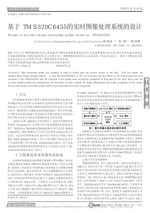
邮局订阅号:82-946360元/年技术创新DSP开发与应用《PLC技术应用200例》您的论文得到两院院士关注基于TMS320C6455的实时图像处理系统的设计Designofreal-timeimageprocessingsystembasedonTS320C6455(1.中国科学院长春光学精密机械与物理研究所;2.北京中国科学院研究生院)李鸿清1,2朱明1鲁剑锋1LIHONGQINGZHUMINGLUJIANFENG摘要:介绍了以TMS320C6455为核心处理器,用FPGA对图像做增强预处理,实现图像数据实时采集,实时处理并通过网络进行传输的视频数字图像处理系统.本文详细介绍了TMS320C6455的特点以及系统的工作原理,阐述了一种基于FPGA的非线性灰度拉伸方法,在系统中实现了图像增强和目标识别.关键词:TMS320C6455FPGA;图像增强;目标识别;灰度拉伸中图分类号:TP391.41文献标识码:BAbstract:Avideoprocessingsystemwasdesignedinordertocollectdataandprocessimagesinrealtime.Andthissystemcantransmittheseimagesthroughnetwork.ItusedtheTMS320C6455asthecoreprocessorandtheFPGAasthepreprocessor.ThemaincharacteroftheTMS320C6455andtheprincipleofthissystemwereparticularlyintroducedinthispaper.Atthesametime,anon-lin-eargraystretchmethodwasproposed,andtheimportantofall,werealizedtheimageenhancementandtargetrecognitioninthissystem.Keywords:imageprocessingsystem,DSP,imageenhancement,targetrecognition文章编号:1008-0570(2007)02-2-0171-031引言实时图像处理系统主要用于图像预处理,图像分割,特征计算,模板匹配,运动分析,目标跟踪等.这些理论和算法已经日渐成熟,现今人们更多的把兴趣转移到算法的实际应用方面.实际应用中,遇到的最大问题就是处理速度的提高,即实时性问题.以DSP为代表的高速数字处理器件的不断更新换代,使得算法的实时性不仅成为可能,而且准确性更高,实时性更强。
针对DDR2-800和DDR3的PCB信号完整性摘要本文章主要涉及到对DDR2和DDR3在设计印制线路板(PCB)时,考虑信号完整性和电源完整性的设计事项,这些是具有相当大的挑战性的。
文章重点是讨论在尽可能少的PCB 层数,特别是4层板的情况下的相关技术,其中一些设计方法在以前已经成熟的使用过。
1.介绍目前,比较普遍使用中的DDR2的速度已经高达800Mbps,甚至更高的速度,如1066Mb ps,而DDR3的速度已经高达1600Mbps。
对于如此高的速度,从PCB的设计角度来讲,要做到严格的时序匹配,以满足波形的完整性,这里有很多的因素需要考虑,所有的这些因素都是会互相影响的,但是,它们之间还是存在一些个性的,它们可以被分类为PCB叠层、阻抗、互联拓扑、时延匹配、串扰、电源完整性和时序,目前,有很多EDA工具可以对它们进行很好的计算和仿真,其中CadenceALLEGROSI-230和Ansoft’sHFSS使用的比较多。
表1:DDR2和DDR3要求比较表1显示了DDR2和DDR3所具有的共有技术要求和专有的技术要求。
2.PCB的叠层(stackup)和阻抗对于一块受PCB层数约束的基板(如4层板)来说,其所有的信号线只能走在TOP和BO TTOM层,中间的两层,其中一层为GND平面层,而另一层为VDD平面层,Vtt和Vref在VDD平面层布线。
而当使用6层来走线时,设计一种专用拓扑结构变得更加容易,同时由于Power层和GND层的间距变小了,从而提高了PI。
互联通道的另一参数阻抗,在DDR2的设计时必须是恒定连续的,单端走线的阻抗匹配电阻50Ohms必须被用到所有的单端信号上,且做到阻抗匹配,而对于差分信号,100Ohms 的终端阻抗匹配电阻必须被用到所有的差分信号终端,比如CLOCK和DQS信号。
另外,所有的匹配电阻必须上拉到VTT,且保持50Ohms,ODT的设置也必须保持在50Ohms。
TMS320C6455高速SRIO接口设计引言数字信号处理技术已广泛应用于通信、雷达、声纳、遥感、图形图像处理和语音处理等领域。
随着现代科技的发展,尤其是半导体工艺的进入深亚微米时代,新的功能强劲的高性能数字信号处理器(DSP)也相继推出,如ADI(美国模拟器件)公司的TigerSHARC系列和TI(德州仪器)公司的C6000系列,但是,要实现对运算量和实时性要求越来越高的DSP 算法,如对基于分数阶傅立叶变换的Chirp信号检测与估计,合成孔径雷达(SAR)成像,高频地波雷达中的自适应滤波和自适应波束形成等算法,单片DSP 仍然显得力不从心。
这些挑战主要涉及两个主题:一是计算能力,指设备、板卡和系统中分别可用的处理资源。
采用多DSP、多FPGA系统,将是提高运算能力的一个有效途径。
二是连接性,从本质上说就是实现不同设备、板卡和系统之间的“快速”数据转移。
对于一些复杂的信息系统,对海量数据传输的实时性提出了苛刻的要求,多DSP之间、DSP与高速AD采集系统、DSP与FPGA间的高速数据传输,是影响信号处理流程的主要瓶颈之一。
TI公司最新推出的高性能TMS320C6455(下文称C6455)处理器,具有高速运算能力的同时集成了高速串行接口SRIO,方便多DSP以及DSP与FPGA之间的数据传输,在一定程度上满足了高速实时处理和传输的要求。
本文在多DSP+FPGA通用信号处理平台的基础上,深入研究了多DSP间,DSP与FPGA间的SRIO 的数据通信和加载技术的软硬件设计与实现。
这些技术包括了目前SRIO接口的各种应用方式,可作为SRIO接口及C6455开发提供参考[1-3]。
1 C6455特性及SRIO标准介绍C6455是目前单片处理能力最强的新型高性能定点DSP,它是TI 公司基于第三代先进VeloviTI VLIW(超长指令字)结构开发出来的新产品。
最高主频为1.2GHz,16位定点处理能力为9600MMAC/s。
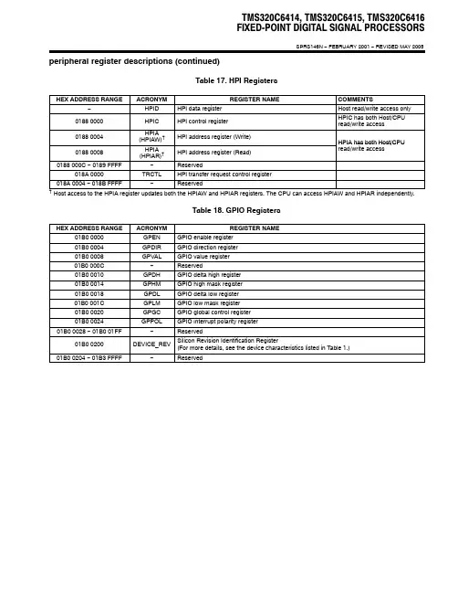
TMS320C6414, TMS320C6415, TMS320C6416FIXED-POINT DIGITAL SIGNAL PROCESSORSSPRS146N − FEBRUARY 2001 − REVISED MAY 2005 peripheral register descriptions (continued)Table 17. HPI RegistersHEX ADDRESS RANGE ACRONYM REGISTER NAME COMMENTS −HPID HPI data register Host read/write access only0188 0000HPIC HPI control register HPIC has both Host/CPUread/write access0188 0004HPIA(HPIAW)†HPI address register (Write)HPIA has both Host/CPU0188 0008HPIA(HPIAR)†HPI address register (Read)read/write access 0188 000C − 0189 FFFF−Reserved018A 0000TRCTL HPI transfer request control register018A 0004 − 018B FFFF−Reserved†Host access to the HPIA register updates both the HPIAW and HPIAR registers. The CPU can access HPIAW and HPIAR independently.Table 18. GPIO RegistersHEX ADDRESS RANGE ACRONYM REGISTER NAME01B0 0000GPEN GPIO enable register01B0 0004GPDIR GPIO direction register01B0 0008GPVAL GPIO value register01B0 000C−Reserved01B0 0010GPDH GPIO delta high register01B0 0014GPHM GPIO high mask register01B0 0018GPDL GPIO delta low register01B0 001C GPLM GPIO low mask register01B0 0020GPGC GPIO global control register01B0 0024GPPOL GPIO interrupt polarity register01B0 0028 − 01B0 01FF−Reserved01B0 0200DEVICE_REV Silicon Revision Identification Register(For more details, see the device characteristics listed in Table 1.)01B0 0204 − 01B3 FFFF−ReservedTMS320C6414, TMS320C6415, TMS320C6416FIXED-POINT DIGITAL SIGNAL PROCESSORSSPRS146N − FEBRUARY 2001 − REVISED MAY 2005signal groups description TRSTGP7/EXT_INT7‡TDITDOTMSTCKEMU0EMU1NMI GP6/EXT_INT6‡GP5/EXT_INT5‡GP4/EXT_INT4‡RESET RSV RSV RSV RSV CLKINCLKMODE1CLKMODE0PLLV EMU2EMU3EMU4EMU5RSV GP7/EXT_INT7‡GP6/EXT_INT6‡GP5/EXT_INT5‡GP4/EXT_INT4‡GP3CLKOUT6/GP2†CLKOUT4/GP1†GP0CLKOUT6/GP2†CLKOUT4/GP1†EMU6EMU7EMU8EMU9EMU10GP15/PRST §GP14/PCLK §GP13/PINTA §GP12/PGNT §GP11/PREQ §GP10/PCBE3§GP9/PIDSEL §CLKS2/GP8†These pins are muxed with the GPIO port pins and by default these signals function as clocks (CLKOUT4 or CLKOUT6) or McBSP2clock source (CLKS2). To use these muxed pins as GPIO signals, the appropriate GPIO register bits (GPxEN and GPxDIR) must be properly enabled and configured. For more details, see the Device Configurations section of this data sheet.†These pins are GPIO pins that can also function as external interrupt sources (EXT_INT[7:4]). Default after reset is EXT_INTx or GPIO as input-only.‡RSV EMU11RSV RSV RSV •••PCI_EN MCBSP2_ENFor the C6415 and C6416 devices, these GPIO pins are muxed with the PCI peripheral pins. By default, these signals are set up to no function with both the GPIO and PCI pin functions disabled . For more details on these muxed pins, see the Device Configurations section of this data sheet. For the C6414 device, the GPIO peripheral pins are not muxed; the C6414 device does not support the PCI peripheral.§Figure 3. CPU and Peripheral Signals。
LTE中基于TMS320C6455 VCP2的Viterbi译码的设计陈发堂;徐炽云
【期刊名称】《广东通信技术》
【年(卷),期】2012(000)010
【摘要】介绍了LTE系统中基于TMS320C6455 DSP芯片上的VCP2协处理器的内部结构及其基本工作原理.并给出了一种增强型EDMA3结构用以提高VCP2协处理器运行速度,并通过在LTE测试平台上测试其性能.实验结果表明,基于TMS320C6455 DSP的VCP2协处理器提高了系统的误码性能,译码速度也高于基于TMS320C6416等其他芯片的协处理器VCP.
【总页数】4页(P71-74)
【作者】陈发堂;徐炽云
【作者单位】重庆邮电大学通信与信息工程学院;重庆邮电大学通信与信息工程学院
【正文语种】中文
【相关文献】
1.水声通信中基于TMS320C6455的Viterbi译码实现 [J], 谢哲;岳志杰
2.应用于LTE-OFDM系统的Viterbi译码在FPGA中的实现 [J], 李小文;林丹
3.一种基于FPGA的多通道复用Viterbi译码器的设计与实现 [J], 庞志锋;刘欣欣;王晓君
4.基于VCP2协处理器的Viterbi译码器实现 [J], 唐贵林;张金菊;侯小毛;
5.一种基于FPGA的Viterbi译码器的研究与设计 [J], 虞亚君; 桑坤; 赵参
因版权原因,仅展示原文概要,查看原文内容请购买。
基于TMS320C6455的高速数字信号处理系统设计摘要:针对高速实时数字信号处理系统设计要求,本文提出并设计了基于dsp+fpga结构的高速数字信号处理系统,采用ti公司目前单片处理能力最强的定点dsp芯片tms320c6455为系统主处理器,fpga作为协处理器。
详细论述了dsp外围接口电路的应用和设计,系统设计电路简洁、实现方便,可靠性强。
关键词:tms320c6455 fpga 数字信号处理系统设计design of high-speed digital signal processing system based on tms320c6455cao jingzhi,he fei,li qiang,ren hui,qin wei (department of tool development,china petroleum logging co.,ltd shaan xi xi’an 710077)abstract:according to the design needs of high-speedreal-time digital signal processing system.the paper puts forward a design of high-speed digital signal processing system based on dsp+fpga structure,adopting ti company fixed-point dsp chip tms320c6455,the currently strongest capacity monolithic processor,for system main processor,and fpga as coprocessor.this paper describs the application and design of dsp periphery circuit interface in detail.the system design has simple circuit and realize convenient, reliability.keywords:tms320c6455 fpga digital signal processing system design随着现代电子技术和计算机技术的飞速发展,高性能数字处理器(dsp)的出现,使得高速数字信号处理系统已应用于越来越多的场合,如通信、雷达、智能交通、图像处理等领域,这些信号处理运算量很大、算法结构复杂,且要求高速实时、高性能、灵活地完成各种处理任务。
基于TMS320 C6455的以太网通信程序的设计摘要:文中介绍了TMS320 C64155 DSP EMAC接口的构成以及工作原理和关键数据结构,参考相关的以太网驱动程序,完成了基于C6455 DSP的以太网通信程序的设计。
该网络通信程序实现了某款信号处理机与上位机之间的高速通信接口。
系统测试结果表明,利用C6455实现的以太网通信接口完全满足系统设计要求,并且系统具有组成简单、系统集成度高等优点。
该方案在其他多功能信号处理设备方面具有一定的应用价值。
关键词:TMS320 C6455;DSP;以太网通信;网络驱动程序随着以太网技术的普及和发展,以太网的通信速率从百兆网逐渐进入了千兆网,甚至万兆网,其通信速率已经满足了常用信号处理机所需要的吞吐率。
而以前仅用来做信号处理的DSP器件逐渐也加入了以太网通信功能,常见的如TI公司的DM642,C6455,C6678等DSP 器件都带有以太网接口,这给一些需要高速通信接口的信号处理板的设计提供了极大的便利。
本文利用某处理板上的TI公司高端DSP器件TMS320 C6455,完成了信号处理板与人机界面之间的高速以太网通信功能。
系统测试结果表明,利用C6455实现的以太网通信接口完全满足系统设计要求,并且系统具有组成简单、系统集成度高等优点。
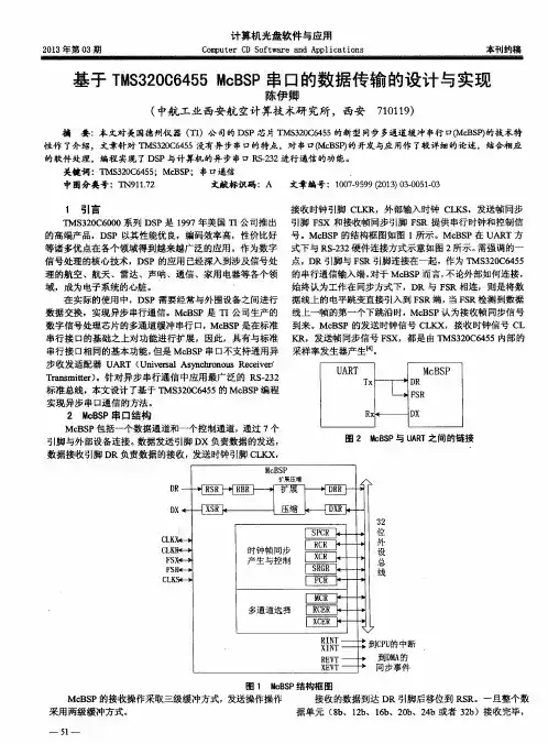
1 硬件平台信号处理板的主要硬件包括两路高速DAC,两路高速ADC以及一块Xilinx V5的FPGA 和一块TMS320 C6455DSP处理器,其中网络通信接口部分主要包括C6455、PHY芯片和RJ45接口,如图1所示。
C6455的EMAC接口与信号板上的PHY芯片以GMII方式连接,支持千兆双工通信模式。
2 C6455 EMAC接口介绍C6455的EMAC接口主要由3部分构成,包括MDIO模块、EMAC模块、EMAC控制模块。
其中MDIO模块通过802.3协议规定的串行通信接口,完成以太网物理层芯片的配置和管理:EMAC模块负责以太网数据包的发送和接收;EMAC控制模块作为DSP核和EMAC接口之间的桥梁,实现DSP核对EMAC模块和MDIO模块的控制。