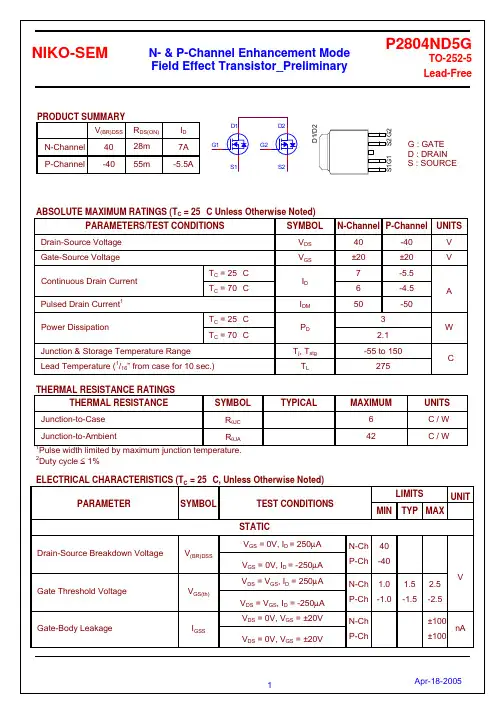
S1QG中文资料
- 格式:pdf
- 大小:751.49 KB
- 文档页数:1


TOSHIBA Field Effect Transistor Silicon P Channel MOS Type (U-MOS III )TPC8107Lithium Ion Battery Applications Notebook PC ApplicationsPortable Equipment Applications· Small footprint due to small and thin package· Low drain-source ON resistance: R DS (ON) = 5.5 m Ω (typ.) · High forward transfer admittance: |Y fs | = 31 S (typ.) · Low leakage current: I DSS = −10 µA (max) (V DS = −30 V)· Enhancement-mode: V th = −0.8 to −2.0 V (V DS = −10 V , I D = −1 mA)Maximum Ratings (Ta = 25°C)Characteristics Symbol Rating UnitDrain-source voltageV DSS -30 V Drain-gate voltage (R GS = 20 k W ) V DGR -30 V Gate-source voltage V GSS ±20 V DC (Note 1) I D -13 Drain currentPulse (Note 1)I DP-52ADrain power dissipation(t = 10 s)(Note 2a) P D 1.9W Drain power dissipation(t = 10 s)(Note 2b)P D 1.0 W Single pulse avalanche energy(Note 3)E AS 219 mJ Avalanche currentI AR-13 ARepetitive avalanche energy(Note 2a) (Note 4)E AR 0.19mJ Channel temperature T ch 150 °C Storage temperature rangeT stg-55 to 150°CNote: For (Note 1), (Note 2), (Note 3) and (Note 4), please refer to thenext page. This transistor is an electrostatic sensitive device. Please handle with caution.Unit: mmJEDEC ― JEITA―TOSHIBA 2-6J1BWeight: 0.080 g (typ.)Circuit ConfigurationThermal CharacteristicsCharacteristics Symbol Max UnitThermal resistance, channel to ambient (t = 10 s)(Note 2a)R th (ch-a) 65.8°C/WThermal resistance, channel to ambient (t = 10 s)(Note 2b)R th (ch-a) 125°C/WMarking (Note 5)(b) Device mounted on a glass-epoxy board (b)Note 3: V DD =-24 V, T ch = 25°C (initial), L = 1.0 mH, R G = 25 W , I AR = -13 A Note 4: Repetitive rating; pulse width limited by maximum channel temperature Note 5: · on lower left of the marking indicates Pin 1.(a) FR-425.4 ´ 25.4 ´ 0.8 (unit: mm)(b)FR-425.4 ´ 25.4 ´ 0.8 (unit: mm)※ Weekly code:(Three digits)Week of manufacture(01 for first week of year, continues up to 52 or 53)Year of manufacture(One low-order digits of calendar year)Electrical Characteristics (Ta = 25°C)Source-Drain Ratings and Characteristics (Ta = 25°C)Typ.MinMax UnitTestConditionCharacteristics SymbolDrain reverse current Pulse (Note 1) I DRP¾ ¾¾-52 A Forward voltage (diode) V DSF I DR=-13 A, V GS= 0 V¾¾ 1.2 VI D – V DSI D – V DSI D – V GSV DS – V GS|Y fs | – I DR DS (ON) – I DF o r w a r d t r a n s f e r a d m i t t a n c e ïY f s ï (S )D r a i n -s o u r c e v o l t a g e V D S (V )Drain-source voltage V DS (V)D r a i n c u r r e n t I D (A )Drain-source voltage V DS (V)D r a i n c u r r e n t I D (A )Gate-source voltage V GS (V)D r a i n c u r r e n t I D (A )Gate-source voltage V GS (V)Drain current I D (A) Drain current I D (A)D r a i n -s o u r c e O N r e s i s t a n c e R D S (O N ) (m W )----------0-4-------0-1-----R DS (ON)– TaI DR – V DSCapacitance – V DSV th – TaP D – TaDynamic input/output characteristicsD r a i n p o w e r d i s s i p a t i o n P D (W )G a t e t h r e s h o l d v o l t a g e V t h (V )Ambient temperature Ta (°C)D r a i n -s o u r c e O N r e s i s t a n c e R D S (O N ) (m W )Drain-source voltage V DS (V)Drain-source voltage V DS (V)C a p a c i t a n c e C (p F )Ambient temperature Ta (°C)Ambient temperature Ta (°C)D r a i n -s o u r c e v o l t a g e V D S (V )G a t e -s o u r c e v o l t a g e V G S (V )Total gate charge Q g (nC)D r a i n r e v e r s e c u r r e n t I D R (A )------80 120 160 2000 40 ---0 40 80 120 160 302010200----0.2 0.4 0.6 0.8 1.0 1.2Drain-source voltage V DS (V)D r a i n c u r r e n t I D (A )Safe operating areaPulse width t w (S)r th - t wN o r m a l i z e d t r a n s i e n t t h e r m a l i m p e d a n c e r t h (°C /W )------· TOSHIBA is continually working to improve the quality and reliability of its products. Nevertheless, semiconductor devices in general can malfunction or fail due to their inherent electrical sensitivity and vulnerability to physical stress. It is the responsibility of the buyer, when utilizing TOSHIBA products, to comply with the standards of safety in making a safe design for the entire system, and to avoid situations in which a malfunction or failure of such TOSHIBA products could cause loss of human life, bodily injury or damage to property.In developing your designs, please ensure that TOSHIBA products are used within specified operating ranges as set forth in the most recent TOSHIBA products specifications. Also, please keep in mind the precautions and conditions set forth in the “Handling Guide for Semiconductor Devices,” or “TOSHIBA Semiconductor Reliability Handbook” etc.. · The TOSHIBA products listed in this document are intended for usage in general electronics applications (computer, personal equipment, office equipment, measuring equipment, industrial robotics, domestic appliances, etc.). These TOSHIBA products are neither intended nor warranted for usage in equipment that requires extraordinarily high quality and/or reliability or a malfunction or failure of which may cause loss of human life or bodily injury (“Unintended Usage”). Unintended Usage include atomic energy control instruments, airplane or spaceship instruments, transportation instruments, traffic signal instruments, combustion control instruments, medical instruments, all types of safety devices, etc.. Unintended Usage of TOSHIBA products listed in this document shall be made at the customer’s own risk. · The information contained herein is presented only as a guide for the applications of our products. No responsibility is assumed by TOSHIBA CORPORATION for any infringements of intellectual property or other rights of the third parties which may result from its use. No license is granted by implication or otherwise under any intellectual property or other rights of TOSHIBA CORPORATION or others.· The information contained herein is subject to change without notice.000707EAARESTRICTIONS ON PRODUCT USE。