
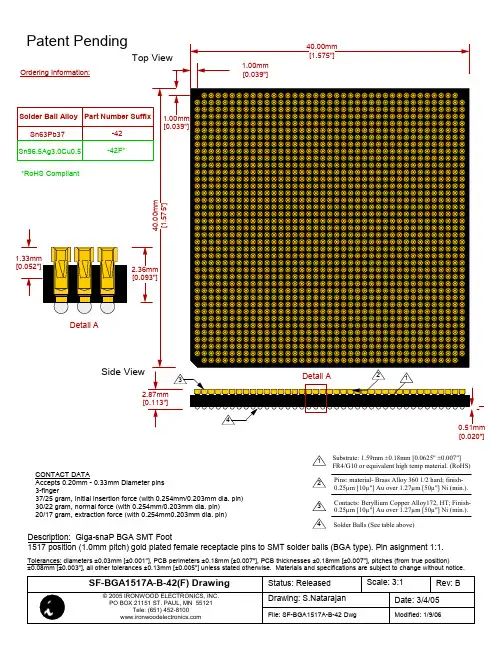
SF-BGA1517A-B-42中文资料
- 格式:pdf
- 大小:248.26 KB
- 文档页数:1

文诚系列技术培训手册清华紫光台式电脑事业部技术支持部2004-06-01目录一、产品特点1.1优良的品质保证1.2出色的结构设计1.3可靠的安全维护二、文诚系列主机配置2.1文诚系列主机配置表三、主板技术规格3.1 精英P6VEMD2主板说明3.2 精英L4S5MG/GX+主板说明3.3 技嘉GA-8I845GV-CH2说明四、驱动程序安装4.1驱动光盘说明4.2驱动程序安装目录一、产品特点文诚系列电脑强调性能价格比,适用于教育、网吧等中低端用户,便于集中管理,统一维护。
1.1优良的品质保证1)通过国家3C认证;2)严格的部件优选体制,所有部件采用业界一线厂商的产品;3)周密的测试全集,保证部件的兼容性,同时保证系统的稳定性;4)五年保修。
1.2出色的结构设计1)立卧两用,根据不同空间随意放置;2)机箱面板模块化设计,根据不同的应用选取不同外观;3)良好的散热设计,确保立卧使用时系统内部热量有效、及时的散发;4)静音设计,减少部件共振,优化风道,降低噪音。
1.3可靠的安全维护1)集成硬盘保护功能,保证硬盘数据的安全,遭到破坏一键恢复;2)同一机型间网络传输功能,维护好一台机器即可通过网络对其他机器进行维护;3)自动维护,无人值班的情况下对整个网络环境中的机器机型维护;4)预留机箱锁孔,防止非法开启机箱。
二、文诚系列主机配置(一)文诚500 文诚800 文诚1000E 文诚1100文诚1200 CPU C3800Celeron 1.8GCeleron 1.8G Celeron 1.8G Celeron 1.8G主板 P6VEMD2L4S5MG/GX+ L4S5MG/GX+ L4S5MG/GX+GA-8I845GV-CH2内存Twinmos 128MDDR333Twinmos 128MDDR333Twinmos 128MDDR333Twinmos 128MDDR333Twinmos 128MDDR333硬盘SeagateST340015ASamsungSV0411N(40GB/5400PRM)SeagateST340015ASamsungSV0411N(40GB/5400PRM)SeagateST340015ASamsungSV0411N(40GB/5400PRM)光驱LG CR-8523B LG GCR-8523B软驱SamsungSFD-321BSamsungSFD-321BSamsungSFD-321B显示卡主板集成主板集成主板集成主板集成主板集成声卡主板集成主板集成主板集成主板集成主板集成网卡主板集成主板集成主板集成主板集成主板集成电源长城 1801-HP 长城 1801-HP 长城 1801-HP 长城 1801-HP 长城 1801-HPCPU风扇主板集成Cool MasterDI4-7H53B/DI4-7H54A-R2Cool MasterDI4-7H53B/DI4-7H54A-R2Cool MasterDI4-7H53B/DI4-7H54A-R2/EC203MBCool MasterDI4-7H53B/DI4-7H54A-R2/EC203MB机箱保利得 EN7472 保利得 EN7472 保利得 EN7472 保利得 EN7472 保利得 EN7472键盘精模 JME7010 精模 JME7010 精模 JME7010 精模 JME7010 精模 JME7010鼠标致伸 M042K0 致伸 M042K0 致伸 M042K0 致伸 M042K0 致伸 M042K0驱动光盘智能驱动光盘V2.0智能驱动光盘V2.0智能驱动光盘V2.0/2.1智能驱动光盘V2.0文诚系列主机配置(二)三、主板技术规格3.1文诚500采用的主板是:精英P6VEMD2,采用VIA CLE266 CE / VT8235 CD 芯片组。


CoolRunner-II Serial Peripheral Interface MasterThe receive full flag (RCV_FULL) is set whenever data is loaded from the SPI receive shiftregister to the SPIRR. This signal is clocked from the system clock and is reset whenever theμC reads data from the SPIRR.SCK Clock LogicThis process generates the SCK output based on the CLKDIV, CPHA, and CPOL settings inthe SPI control register. The clock frequency of the SCK signal is determined by dividing downthe input clock based on the entries in the control register. The signal, SCK_INT is the internalSCK used to clock serial data out of the device and is continually generated. The SPI Controlstate machine is synchronized to this internal signal. The signal SCK_1 represents SCK whenCPHA = 1 and the signal SCK_0 represents SCK when CPHA = 0. The SPI control statemachine generates the masks for these clocks (CLK0_MASK, CLK1_MASK) so that the outputSCK has the correct phase relationship with the data and is held in its inactive state when thereis no data to be transferred. A representation of the logic required to generate the SCK signaloutput to the SPI bus is shown in Figure8.Figure 8: SCK Clock Generation LogicSPI Shift RegistersSPI Transmit Shift RegisterThe SPI transmit shift register is an 8-bit loadable shift register containing SPI data. This shiftregister is loaded from the SPI Transmit Register (SPITR) via a load signal generated by theSPI Control state machine and is clocked by the rising edge of SCK_INT. The data shifting outis the MOSI data. Note that in Figure8, SCK_OUT is one SYS_CLK delay from SCK_INT.Therefore, it is necessary to delay the data being shifted out from the SPI transmit shift registerby one SYS_CLK as well so that the relationship between MOSI and SCK_OUT is maintained. XAPP386 (v1.0) December 12, 2002White Paper: CoolRunner-II CPLDs in Cell Phone Handsets/Terminals But what about new applications that are not in this group? There are applications yet to come that we can envision, but whose exact specifications we cannot wholly anticipate. Designing for their arrival is sometimes called “future proofing.”It is true that some applications are better served by microprocessor code dropped into on board EPROM, but that can only happen as long as the processor bandwidth is available for the application. If this cannot be done, either more processors or additional silicon needs to be added. Either way, the application will need to interface into the phone bus network, and that will require programmable logic, very low power programmable logic.MediPhone—A Speculative Example To drive home some of these ideas, consider an idea for a product that probably does not exist today, but easily could in the near future. It will be marketed under the name “MediPhone” and will target segments of the population that require quick medical support. This would include the growing population of elderly citizens (frequently with enough money to buy these) as well as handicapped people needing close monitoring. See Figure4 for an “artist” conception of this futuristic phone.MediPhone works like this:1. A heart attack (or other medical emergency occurs)2.The victim or friend dials Emergency (911 in the U.S.)3.Personnel receiving the call at a medical facility recognize the phone is“MediPhone” equipped and extract the geographic location of the emergency using GPS4.The medic directs the friend to place the cell phone on the victim’s face5. A video camera scans the Iris for dilation to determine shock level6.The friend is directed to attach small electrodes to the forehead/ear and chest ofthe victim, where pulse is taken and EEG/EKG measurements are driven into the Internet. Everything is attached to the phone.Figure 4:MediPhone Block DiagramWP198 (v1.1) July 4, 2005。
Board InstallationIntroductionThis appendix provides the information required to install, program, debug, and deploy a Xilinx® accelerator board to execute applications created with the SDx® environment. The SDx environment executes in hardware using one of the FPGA boards listed in the application.Installing a BoardThe KCU1500 card is a high-performance reconfigurable computing card for data center applications and includes these features:•XCKU1500-2FLVB2104E FPGA •Four 4GB DDR4 banks (16GB total)The following sections describe how to install a board.Step 1: Set Up the Card and Computer1.Make sure the host computer is completely turned off.2.Install the FPGA board in an open PCIe® slot on the host computer.3.Turn on the host computer.Note:Follow the host computer manufacturer recommendations to ensure proper mountingand adequate cooling.找FPGA 和CPLD 可编程逻辑器件,上赛灵思半导体(深圳)有限公司Step 2: Prepare Board Installation FilesThe SDx environment provides the xbinst utility, which generates firmware and driver files for the target board plugged into the deployment computer.1.Run the following commands to prepare files for the target board installation.See the SDx Command and Utility Reference Guide (UG1279) [Ref6] for more details on the xbinst utility. Depending on the target location, some commands must be run with root or sudo privilege. Otherwise, access permissions must be changed to enable read access for all users on that system.e the following commands to create the deployment area inside/opt/dsa/:$ mkdir /opt/dsa$ mkdir /opt/dsa/xilinx_vcu1525_dynamic_5_1$ cd /opt/dsa/xilinx_vcu1525_dynamic_5_1Note:To install and deploy the KCU1500 files, use xilinx_kcu1500_dynamic_5_0 in step 2 and 3.3.Execute xbinst to install the files needed for the deployment machine. Output similarto the following is displayed:$ xbinst --platform xilinx_vcu1525_dynamic_5_1 -d .****** xbinst v2018.2 (64-bit)**** SW Build 2254440 on Sun Jun 10 18:05:35 MDT 2018** Copyright 1986-2018 Xilinx, Inc. All Rights Reserved.Attempting to get a license: ap_openclFeature available: ap_openclINFO: [XBINST 60-895] Target platform:/opt/Xilinx/SDx/2018.2/platforms/xilinx_vcu1525_dynamic_5_1/xilinx_vcu1525_dynamic_ 5_1.xpfmINFO: [XBINST 60-267] Packaging for PCIe...INFO: [XBINST 60-1032] Extracting DSA to./.Xil/xbinst-1273/xilinx_vcu1525_dynamic_5_1INFO: Adding section [FIRMWARE (3)] using: 'mgmt' (23192 Bytes)INFO: Adding section [SCHED_FIRMWARE (5)] using: 'sched' (9748 Bytes)Successfully completed 'xclbincat'INFO: [XBINST 60-268] Packaging for PLETEINFO: [XBINST 60-667] xbinst has successfully created a board installation directory at /opt/dsa/xilinx_vcu1525_dynamic_5_1.The files are installed in this location:/opt/dsa/xilinx_vcu1525_dynamic_5_1/xbinst:Make a note of the deployment location area because it is required at a later stage.This section refers to this location as the <xbinst-area> or as the deploymentdirectory.4.Install the drivers as described in Step 3: Install Board Drivers.Capabilities: <access denied>Kernel driver in use: xoclKernel modules: xocl03:00.1 Serial controller: Xilinx Corporation Device 6a8f (prog-if 01 [16450]) Subsystem: Xilinx Corporation Device 4351Control: I/O+ Mem+ BusMaster- SpecCycle- MemWINV- VGASnoop- ParErr- Stepping- SERR- FastB2B- DisINTx-Status: Cap+ 66MHz- UDF- FastB2B- ParErr- DEVSEL=fast >TAbort- <TAbort- <MAbort- >SERR- <PERR- INTx-Region 0: Memory at f4000000 (32-bit, non-prefetchable) [size=32M]Region 2: Memory at f8020000 (32-bit, non-prefetchable) [size=128K]Region 4: Memory at f8000000 (32-bit, non-prefetchable) [size=128K]Capabilities: <access denied>Kernel driver in use: xclmgmtKernel modules: xclmgmt。