三星 TECHWIN_QSA_Rev_4.1_CHI(08)
- 格式:xls
- 大小:126.00 KB
- 文档页数:14

Samsung Exynos 4 Quad(Exynos 4412)RISC MicroprocessorRevision 1.00October 2012 U s e r's M a n u a l2012 Samsung Electronics Co., Ltd. All rights reserved.Important NoticeSamsung Electronics Co. Ltd. (“Samsung”) reserves the right to make changes to the information in this publication at any time without prior notice. All information provided is for reference purpose only. Samsung assumes no responsibility for possible errors or omissions, or for any consequences resulting from the use of the information contained herein.This publication on its own does not convey any license, either express or implied, relating to any Samsung and/or third-party products, under the intellectual property rights of Samsung and/or any third parties.Samsung makes no warranty, representation, or guarantee regarding the suitability of its products for any particular purpose, nor does Samsung assume any liability arising out of the application or use of any product or circuit and specifically disclaims any and all liability, including without limitation any consequential or incidental damages.Customers are responsible for their own products and applications. "Typical" parameters can and do vary in different applications. All operating parameters, including "Typicals" must be validated for each customer application by the customer's technical experts.Samsung products are not designed, intended, or authorized for use in applications intended to support or sustain life, or for any other application in which the failure of the Samsung product could reasonably be expected to create a situation where personal injury or death may occur. Customers acknowledge and agree that they are solely responsible to meet all other legal and regulatory requirements regarding their applications using Samsung products notwithstanding any information provided in this publication. Customer shall indemnify and hold Samsung and its officers, employees, subsidiaries, affiliates, and distributors harmless against all claims, costs, damages, expenses, and reasonable attorney fees arising out of, either directly or indirectly, any claim (including but not limited to personal injury or death) thatmay be associated with such unintended, unauthorizedand/or illegal use.WARNING No part of this publication may be reproduced, stored in a retrieval system, or transmitted in any form or by any means, electric or mechanical, by photocopying, recording, or otherwise, without the prior written consent of Samsung. This publication is intended for use by designated recipients only. This publication contains confidential information (including trade secrets) of Samsung protectedby Competition Law, Trade Secrets Protection Act and other related laws, and therefore may not be, in part or in whole, directly or indirectly publicized, distributed, photocopied or used (including in a posting on the Internet where unspecified access is possible) by any unauthorized third party. Samsung reserves its right to take any and all measures both in equity and law available to it and claim full damages against any party that misappropriates Samsung’s trade secrets and/or confidential information.警告本文件仅向经韩国三星电子株式会社授权的人员提供,其内容含有商业秘密保护相关法规规定并受其保护的三星电子株式会社商业秘密,任何直接或间接非法向第三人披露、传播、复制或允许第三人使用该文件全部或部分内容的行为(包括在互联网等公开媒介刊登该商业秘密而可能导致不特定第三人获取相关信息的行为)皆为法律严格禁止。
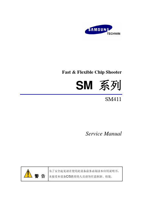
Fast & Flexible Chip Shooter SM系列SM411Service Manual警告为了安全起见请在使用此设备前务必阅读本应用说明书。
未接受本设备C/S教育的人员请勿任意拆卸、组装。
Fast & Flexible Chip ShooterSM 系列SM411Service ManualVersion 1发行: 2007 年 6 月 (MMI version 0.913)三星泰科株式会社严禁复制Calibration第 3 章. C alibration 本过程介绍安装设备、Warming-Up执行后必须执行的校正过程。
执行校正之前需要确认或先行的作业为如下。
I/O Test确认及补正Mirror OffsetNozzle Check及System Constant的Vacuum Check OptionNozzle Check及System Constant的校正Tool Option:[80]号 “1” (default)1234ANC Type确认确认空压是否异常3-1Samsung Component Placer SM411 Service Manual3-23.1. Mirror Offset 确认及补正为清晰显示通过反射镜显示在fly camera 的影像,应设置Swing Mirror Offset 。
以下是Swing Mirror Offset 设置过程。
1. 操作示教框把Head Assembly 最大限度地往两边移动。
2. 在’Sys. Setup’菜单选择‘Calib.’ 下位菜单后,点击<1.Axis Home Calibration> 按钮后, 请在‘System Axis Home & Limit Info.’对话框选择‘H1F-M1’。
2354Calibration 3.在‘Tools’快捷菜单选择‘Manual Tool’,在‘Manual Control’对话框的<Axis>组合框选择‘Mirror’。

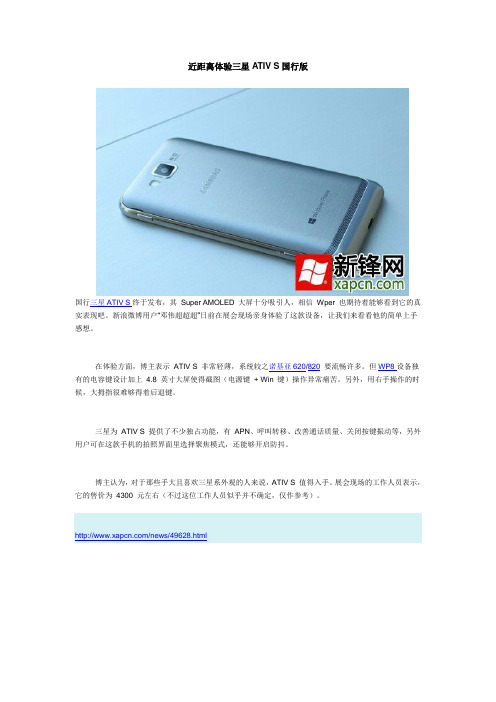
近距离体验三星A TIV S国行版
国行三星ATIV S终于发布,其Super AMOLED 大屏十分吸引人,相信Wper 也期待着能够看到它的真实表现吧。
新浪微博用户“邓伟超超超”日前在展会现场亲身体验了这款设备,让我们来看看他的简单上手感想。
在体验方面,博主表示ATIV S 非常轻薄,系统较之诺基亚620/820要流畅许多。
但WP8设备独有的电容键设计加上 4.8 英寸大屏使得截图(电源键+ Win 键)操作异常痛苦。
另外,用右手操作的时候,大拇指很难够得着后退键。
三星为ATIV S 提供了不少独占功能,有APN、呼叫转移、改善通话质量、关闭按键振动等,另外用户可在这款手机的拍照界面里选择聚焦模式,还能够开启防抖。
博主认为,对于那些手大且喜欢三星系外观的人来说,ATIV S 值得入手。
展会现场的工作人员表示,它的售价为4300 元左右(不过这位工作人员似乎并不确定,仅作参考)。
/news/49628.html。

CAUTIONREAD ME FIRST Failure to follow these procedures will cause your system to not recognize the new CPU/Memory board.Firmware on all boards and assemblies must be at the same level as the new CPU/Memory board.Sun Fire ™ High-End and Midrange Systems UltraSPARC ® IV CPU/Memory Board Upgrade RequirementsSun Fire E25K/E20K SystemsSun Fire 15K/12K SystemsSun Fire E6900/E4900 SystemsSun Fire 6800/4800 Systems!Note –If sold as a field-replaceable unit (FRU),a CPU/Memory board is for replacement use only .FRUs must not be used to upgrade CPU performance in systems.Such usage can violate United States export regulations.Note –UltraSPARC ®IV CPU/Memory boards are not supported in Sun Fire™4810/3800systems.Only earlier versions of CPU/Memory boards are supported in Sun Fire 4810/3800systems.Additional Hardware Requirements for Sun Fire 6800/4800SystemsSun Fire™6800/4800systems require additional hardware upgrades if you upgrade to UltraSPARC IV CPU/Memory boards:■Sun Fire 6800system:upgrade all six power supplies (PS0through PS5)to part number 300-1595-xx.Also install an EMI gasket kit,part number 560-2755-xx in the card cage.■Sun Fire 4800system:upgrade all three power supplies (PS0through PS2)to part number 300-1596-xx.Also upgrade the fan trays:FT0(bottom left)to part number 540-5998-xx,FT1(top)to part number 540-5997-xx,and FT2(bottom right)to part number 540-5999-xx.Caution –The Sun Fire 6800/4800system might shut down if you do not install the additional upgrades that are required for theUltraSPARC IV CPU/Memory boards.♦To determine if the hardware upgrades are already installed:■Use the system controller showfru command to see the manufacturing record of FRU part numbers.This command is available with firmware version 5.18.1and later.■Alternatively,you can find the part numbers on the device labels.Firmware and OS Minimum RequirementsNote –If your system requires a software upgrade and a firmware upgrade,upgrade the firmware first.Upgrade the software second.Install new CPU/Memory boards only after you have upgraded the firmware and software.schostname :SC>showfru -r manrSun Fire E6900/E4900systems and upgraded Sun Fire6800/4800systems require these versions:■Firmware level5.18.1or subsequent compatible versions.■Solaris82/04Operating System or subsequent compatible versions. Sun Fire E25K/E20K systems and upgraded Sun Fire15K/12K systems require these versions:■SMS1.4.1or subsequent compatible versions.■SMS1.4.1patch1178660-04.■Solaris82/04Operating System or subsequent compatible versions. Note–Patches can be found at:Installation information,Release Notes and README files are included in the patch download.Checking Firmware on Boards and Assemblies♦When installing new CPU/Memory boards,use the showboards command to determine if the firmware needs to be updated:schostname:SC>showboards -p promsIf an update is required,use the system controller flashupdate command as shown below.Upgrading FirmwareUpgrade thefirmware and real time operating system(RTOS)images only if the image to install is different than the image that is already installed.♦To install the firmware upgrade,use the flashupdate command for your specific system.■For Sun Fire E6900/E4900or Sun Fire6800/4800systems:schostname:SC> flashupdate -f URL all rtos■For Sun Fire E25K/E20K or Sun Fire15K/12K systems:schostname:SC> flashupdate -f URL -d domain_idFor details on using the flashupdate command,refer to the system controller manual for your product.Sun Microsystems, Inc.Part No. 819-1279-10, Rev. AJanuary 2005Accessing Sun DocumentationYou can view,print,or purchase a broad selection of Sun documentation,including localized versions,at:/documentationContacting Sun Technical SupportIf you have technical questions about this product that are not answered in this document,go to:/service/contactingSun Welcomes Your CommentsSun is interested in improving its documentation and welcomes your comments and suggestions.You can submit your comments by going to:/hwdocs/feedbackPlease include the title and part number of your document with your feedback:Sun Fire High-End and Midrange Systems UltraSPARC IV CPU/Memory Board Upgrade Requirements ,part number 819-1279-10Copyright 2004Sun Microsystems,Inc.All rights e is subject to license terms.Third-party software,including font technology,is copyrighted and licensed from Sun suppliers.Portions may be derived from Berkeley BSD systems,licensed from U.of CA.Sun,Sun Microsystems,the Sun logo,and Solaris are trademarks or registered trademarks of Sun Microsystems,Inc.in the U.S.and in other countries.All SPARC trademarks are used under license and are trademarks or registered trademarks of SPARC International,Inc.in the U.S.and in other ernment Rights—Commercial ernment users are subject to the Sun Microsystems,Inc.standard license agreement and applicable provisions of the FAR and its supplements.Copyright 2004Sun Microsystems,Inc.Tous droits réservés.Distribuépar des licences qui en restreignent l’utilisation.Le logiciel détenu par des tiers,et qui comprend la technologie relative aux polices de caractères,est protégépar un copyright et licenciépar des fournisseurs de Sun.Des parties de ce produit pourront être dérivées des systèmes Berkeley BSD licenciés par l’Universitéde Californie.Sun,Sun Microsystems,le logo Sun,et Solaris sont des marques de fabrique ou des marques déposées de Sun Microsystems,Inc.aux Etats-Unis et dans d’autres pays.Toutes les marques SPARC sont utilisées sous licence et sont des marques de fabrique ou des marques déposées de SPARC International,Inc.aux Etats-Unis et dans d’autres pays.。
对于某一特性的调节步骤(仅适用三星S800数码相机)⑴调整介绍在更换了S800的某一部件后,对于每一个特性必须做相应调整。
对于某一部件的更换必须按照下表描述的做相应的调整。
每一程序段后以“;”结束。
在具体调节时对于不具备业余测试条件的方式根据情况取舍。
⑵功能板设置—OB SETTING在更换主板后,屏幕调整成黑色。
调整步骤a…把相应调整文件复制到SD卡里。
b…把包含程序文件的SD卡插入到相机内并开启相机。
c…当调整完成后,相机将自动关闭。
程序文件STS2_83ADJ.txt⑷CCD坏点—CCD DEFECT PIXEL可对相机内的CCD坏点进行补偿。
在更换主板和CCD组件后调节坏点。
在运行完燃烧程序后,对CCD内坏点进行适当的调整。
调整步骤a…把相应调整文件复制到SD卡里。
b…把包含程序文件的SD卡插入到相机内并开启相机。
c…调整将自动引导。
d…当调整完成后,相机将自动关闭。
⑸齿间隙调节—BACK LASH ADJ.当镜筒改变转向时能够进行误差补偿。
在更换主板,镜筒和CCD后调节齿间隙。
调整步骤a…把相应调整文件复制到SD卡里。
b…把包含程序文件的SD卡插入到相机内并开启相机。
c…在LCD上显示调整信息并启动自动调节。
d…当调整完成后,相机将自动关闭。
程序文件STS2_83ADJ.txt⑽聚焦调整PUNT ADJ.—FOCUS ADJ.为达到镜头的最佳聚焦控制,判断AF的搜索范围。
调整的目的:在更换主板或镜头组件后调整PUNT。
需要设备:焦距调整图和三脚架。
调整步骤a…给相机安上三脚架。
对焦范围:正常80cm~无穷远。
业余调试可在2m左右拍照。
依据产品指定的距离镜头朝向一个更远的目标。
b…根据特定的调整安装相机。
特定目标的距离。
相机对准建筑物的方向或更远距离的目标(不使用图表)。
PUNT调整用作参考点的物体或从一个更远的距离诸如建筑物或户外目标。
物体没有诸如单色的天和白雪覆盖的风景参照物。
在产品规格范围内对准更远一点的地方。
如何硬格式化恢复出厂设置 Samsung Galaxy A5
Samsung Galaxy A5 -硬格式化恢复出厂设置
撰写者: ZFix
介绍
Samsung Galaxy A5
若您的手机在锁屏下不能通过登入Google账户解锁或您的手机操作系统出现故障无法进行初始化时。
[video: https:///watch?v=KdwqAZng2v4]
这一系列操作将会抹除您设备上的系统偏好设置、用户数据、第三方应用及第三方应用的应用数据,而经过该操作后您的手机操作系统将会回到最初(您刚买到时)的状态。
步骤 1 — 如何硬格式化恢复出厂设置 Samsung Galaxy A5
把手机关机
按住音量上键,主页键和电源键。
当您看到Galaxy标志时只松开电源按钮。
本恢复设置不可逆。
步骤
2
使用音量上键/下键进行导航并用电源键进行选择。
从安卓系统恢复菜单中选择:
清除数据/回复出厂设置
选择是--清除所有用户数据
现在重启系统
就这样。
你搞定了吗?。
Table of Contents ................................................................................................................................................................... 3 List of Figures .......................................................................................................................................................................... 4 List of Tables ........................................................................................................................................................................... 4 Version History .. (5)Handling Guide ....................................................................................................................................................................... 6 ARTIK 530 Development Board Overview (7)features (7)Block diagram ....................................................................................................................................................................................... 8 Mechanical Drawings ........................................................................................................................................................................... 9 ARTIK 530 Module ................................................................................................................................................................ 11 ARTIK 530 Module Specification ........................................................................................................................................................ 11 ARTIK 530 Development Board Interposer Board .. (12)Interposer Board Boot mode Configuration .................................................................................................................................... 13 USB OTG ............................................................................................................................................................................................... 14 HDMI 1.4a ............................................................................................................................................................................................ 14 LVDS ..................................................................................................................................................................................................... 15 Ethernet................................................................................................................................................................................................ 15 Antenna ................................................................................................................................................................................................ 16 ARTIK 530 Development Board Platform Board .. (17)Configuration of External Power Source .......................................................................................................................................... 18 SD-Card Interface................................................................................................................................................................................ 19 EarJack Interface ................................................................................................................................................................................. 19 MIPI DSI/CSI Interface ......................................................................................................................................................................... 19 USB Host 2.0 Interface ....................................................................................................................................................................... 21 Connector to IF Board Interface ........................................................................................................................................................ 22 ARTIK 530 Development Environment IF Board .............................................................................................................. 23 Preview on the ARTIK IF board .......................................................................................................................................................... 23 Configuration of external Power Source .......................................................................................................................................... 24 ARTIK 530 Development Board Booting (25)Serial Port Connection ....................................................................................................................................................................... 25 Terminal Emulator Installation ......................................................................................................................................................... 26 Power on the ARTIK 530 Development Board.................................................................................................................................. 27 Legal Information .. (29)Figure 1. Preview of the ARTIK 530 Development Board .................................................................................................... 7 Figure 2. ARTIK 530 Development Board .............................................................................................................................. 8 Figure 3. Mechanical Drawing ARTIK 530 Development Board and Interposer Board all dimensions are in [mm] .. 9 Figure 4. Mechanical Drawing ARTIK 530 Development Board Platform Board all dimensions are in [mm] .......... 10 Figure 5. ARTIK 530 Development Board Interposer Board Left Top Side, Right Bottom Side .................................. 12 Figure 6. ARTIK 530 Development Board Booting Switch Location ................................................................................ 13 Figure 7. USB OTG Interface location on the Interposer Board ...................................................................................... 14 Figure 8. HDMI 1.4a Interface location on the Interposer Board ................................................................................... 14 Figure 9. LVDS Interface location on the Interposer Board ............................................................................................. 15 Figure 10. Ethernet Interface location on the Interposer Board .................................................................................... 15 Figure 11. Antenna location on the Interposer Board ..................................................................................................... 16 Figure 12. ARTIK 530 Development Board Platform Board Left Bottom Side, Right Top Side ................................... 17 Figure 13. Jumper Interface locations JP1-JP4 on Connectors J702, J703 of the Platform Board ............................... 18 Figure 14. SD-Card Interface location on the Platform Board ........................................................................................ 19 Figure 15. Ear Jack Interface location on the Platform Board ......................................................................................... 19 Figure 16. MIPI DSI Interface location on the Platform Board ........................................................................................ 20 Figure 17. MIPI CSI Interface Location on the Platform Board ....................................................................................... 20 Figure 18 USB2.0 Interface location on the Platform Board ........................................................................................... 21 Figure 19. Expansion Connector Interface location on the Platform Board ................................................................. 22 Figure 20. ARTIK 530 Development Board IF Board ......................................................................................................... 23 Figure 21. Jumper Interface locations J20, J21 on the IF Board ....................................................................................... 24 Figure 22. Typical Linux® Serial Console ........................................................................................................................... 25 Figure 23. USB Serial Cable hooked up to the Platform Board ....................................................................................... 26 Figure 24 Connection Power adaptor with development Board .................................................................................... 27 Figure 25. Power switch location on the development Board ........................................................................................ 28 Figure 26. Power button location on the development Board (28)Table 1. Main Features of the ARTIK 530 Module ............................................................................................................. 11 Table 2. Boot option that can be set on the Interposer Board ....................................................................................... 13 Table 3 Antenna spec ........................................................................................................................................................... 16 Table 4. Connector J2 ............................................................................................................................................................ 23 Table 5. Connector J3 (24)Precaution against Electrostatic DischargeWhen using the Samsung ARTIK ™ 530 Development Board, ensure that the environment is protected against static electricity: ContaminationDo not use the ARTIK 530 Development Board in an environment exposed to dust or dirt adhesion. Temperature/HumidityThe ARTIK 530 Development Board is sensitive to:1. Environment2. Temperature3. HumidityHigh temperature or humidity deteriorates the characteristics of ARTIK 530 Development Board, therefore, do not store or use the ARTIK 530 Development Board under such conditions. Mechanical ShockDo not to apply excessive mechanical shock or force to the ARTIK 530 Development Board. ChemicalDo not expose the ARTIK 530 Development Board to chemicals. Exposure to chemicals leads to reactions that deteriorate the characteristics of the ARTIK 530 Development Board. EMS (Electro Magnetic Susceptibility)Strong electromagnetic waves or magnetic fields may affect the characteristics of the ARTIK 530 Development Board during the operation under insufficient PCB circuit design for Electro Magnetic Susceptibility (EMS).The ARTIK 530 Development Board consists of one Interposer Board, one Platform Board and one IF Board. The Interposer Board does include the ARTIK 530 Module. The ARTIK 530 Development Board is an affordable approach for developing an IoT solution. Figure 1 shows the form factors of the various boards that make up the ARTIK 530 Development Board.Figure 2 shows the block diagram of the ARTIK 530 Development Board, if you want more information on the ARTIK 530 Module please consult the ARTIK 530 Module Datasheet.Figure 3 and Figure 4 show the ARTIK 530 Development Board Interposer Board and the Platform Board respectively.The ARTIK 530 Development Board contains the ARTIK 530 Module. This section will describe some of the main features of this module. For more information on the ARTIK 530 Module please consult the ARTIK 530 Module datasheet.The ARTIK 530 Module is designed for IoT devices and it contains a lot of functions based on a Linux ®system. Not only multimedia functions but also network functions for example 802.11 or ZigBee ®. In addition the ARTIK 530 Module has mass storage functionality and its own security solution. Table 1 shows the main features of the ARTIK 530 Module that is part of the ARTIK 530 Development Board.®®®®The Interposer Board as depicted in Figure 5 highlights the most important components on the Interposer board.This section describes the various boot modes that are supported on the ARTIK 530 Development Board. Table 2 and Figure 6 show how to manipulate SW402 and where SW402 is located on the Interposer Board to set the various booting options that are available on the ARTIK 530 Development Board.When ‘eMMc 1st Boot’ is selected as a booting option, the system will first try to boot from eMMc, if this fails the system will search for an SD Card to boot from. If booting from the SD-Card also fails the system tries to boot from USB. When choosing the SD-Card booting option, the system starts with booting from SD, and if this fails will continue to try a USB boot. When USB is selected as the booting mechanism of choice, only a USB boot will be attempted.The Interposer board has one USB OTG connector located as can be seen in Figure 7.The Interposer board has one HDMI 1.4a connector (Micro D-Type) located as can be seen in Figure 8. The following video formats are supported:1.480p/************/60Hz,576p/576i@50Hz2.720p/720i @50Hz/59.94Hz/60HzThe Interposer board has one LVDS Interface containing 5x data channels and one clock channel, its location can be seen in Figure 9. The available maximum resolution is 1920x1080@60fps.The Interposer board has one Ethernet Interface, its location can be seen in Figure 10. The Ethernet Interface is based on 802.3az-2010 complying to the Energy Efficient Ethernet (EEE) standard. The maximum theoretical speed of the interface is 1000Mbps.If 802.11 or Bluetooth® functionality is required, the antenna which is enclosed as part of the ARTIK 530 Development Kit has to be attached to the Interposer board as depicted in Figure 11. More details on the antenna spec is given in Table 3.The Platform Board as depicted in Figure 12 highlights the most important components on the Interposer board.Through selection of the Jumpers JP1-JP4, located on J702, J703, the power source can be selected. When power is provided from a DC-5V Adapter or a Battery, all jumpers are in the 1-2 position. When power is provided from the DC-5V Adapter and at the same time a battery is connected that is being charged (Battery Charging Mode), all jumpers are in the 2-3 position. When the jumpers [JP1-JP4] are in the 1-2 position, (DC-5V Adapter mode or Battery mode) either connect a battery or the DC-5V adapter but never both at the same time. When the jumpers [JP1-JP4] are in the 2-3 position, (Battery Charging Mode) connect both a battery and the DC-5V Adapter.Figure 13 shows the default settings and how to switch between the settings. When the ARTIK 530 Development Board is used with an external power adapter make certain that you use a 5V-5A adapter with a 2.1x5.5mm plug.The Platform board has one SD-CARD interface supporting SD3.0 located as can be seen in Figure 14.The Platform board has one 4 pin ear jack interface supporting stereo audio as can be seen in Figure 15.The Platform board has one MIPI DSI and one MIPI CSI interface. The location of the DSI Display interface can be seen in Figure 16. The location of the MIPI CSI interface can be seen in Figure 17.The MIPI DSI interface can operate at a maximumresolution of WUXGA (1920x1200), whereas the MIPI CSI interface can have a static resolution of 5M pixels or a dynamic resolution for video capturing of 1080P.The Platform board has one USB 2.0 Interface. The location of the USB 2.0 interface can be seen in .The Platform board has one expansion connector that can be seen in Figure 19. This connector enables for expansion possibilities.Figure 20 shows the highlights of the connector IF board. In addition Table 4 with J2 and Table 5 with J3 show the pinout of the connectors with its meaning.Through selection of the Jumpers J20 and J21 you can choose the IO power source (I 2C, UART GPIO) or the XGPIO power source of either, 1.8V, 3.3V or 5V. Figure 21 shows how to set the various jumpers to switch between power sources.This section will describe how to start working with your ARTIK 530 Development Environment by setting up a serial connection on your development PC and booting up the ARTIK 530 Development Environment.As a first step we will select a serial console to communicate with the ARTIK 530 Module that is located on the ARTIK 530Development Environment. You can use a typical Linux ®serial console as depicted in Figure 22, using the serial connector. If your PC does not have a serial port, use the micro-USB B serial cable instead. To use the serial USB cable you need to install the associated device driver. Figure 23 depicts the USB serial cable and where it is hooked up to the Platform Board.Setting up a connection with the ARTIK 530 Module can be done in a wired or wireless manner. Here we choose to install PuTTY a free serial console. The software can be downloaded from /. Once downloaded go through the following steps:1.Open the device manager on the control panel.2.When using a PC install the USB to Serial driver. The driver can be found at the following location:(/Drivers/CDM/CDM21218_Setup.zip). For other drivers please visit(/Drivers/D2XX.htm).3.Check the COM port number on your PC when you connect the USB serial cable. In our case the COM port allocated4.a.Set the “Serial line” as the COM port number found in step 3.b.Set the COM speed to "115200".c.Set the connection type to "Serial".d.Save the session under ARTIK-Pro.5.Select your saved session and click th e “Open” button.To power up the ARTIK 530 Development Environment you first have to connect the power adapter and the Platform Board as shown in Figure 24. In addition make certain that the jumpers JP1-JP4 located on the Platform Board are set in state 1-2 see Configuration of External Power Source section for details.Turn on the power switch as shown in Figure 25.Once the power switch is turned on, push the power button (SW2), as depicted in Figure 26, for about 1 second. Once released the booting process will start and you should see booting messages from your console, using the serial connection that you previously established.INFORMATION IN THIS DOCUMENT IS PROVIDED IN CONNECTION WITH THE SAMSUNG ARTIK ™ DEVELOPMENT BOARD AND ALL RELATED PRODUCTS, UPDATES, AND DOCUMENTATION (HEREINAFTER “SAMSUNG PRODUCTS”). NO LICENSE, EXPRESS OR IMPLIED, BY ESTOPPEL OR OTHERWISE, TO ANY INTELLECTUAL PROPERTY RIGHTS IS GRANTED BY THIS DOCUMENT. THE LICENSE AND OTHER TERMS AND CONDITIONS RELATED TO YOUR USE OF THE SAMSUNG PRODUCTS ARE GOVERNED EXCLUSIVELY BY THE SAMSUNG ARTIK ™ DEVELOPER LICENSE AGREEMENT THAT YOU AGREED TO WHEN YOU REGISTERED AS A DEVELOPER TO RECEIVE THE SAMSUNG PRODUCTS. EXCEPT AS PROVIDED IN THE SAMSUNG ARTIK ™ DEVELOPER L ICENSE AGREEMENT, SAMSUNG ELECTRONICS CO., LTD. AND ITS AFFILIATES (COLLECTIVELY, “SAMSUNG”) ASSUMES NO LIABILITY WHATSOEVER, INCLUDING WITHOUT LIMITATION CONSEQUENTIAL OR INCIDENTAL DAMAGES, AND SAMSUNG DISCLAIMS ANY EXPRESS OR IMPLIED WARRANTY, ARISING OUT OF OR RELATED TO YOUR SALE, APPLICATION AND/OR USE OF SAMSUNG PRODUCTS INCLUDING LIABILITY OR WARRANTIES RELATED TO FITNESS FOR A PARTICULAR PURPOSE, MERCHANTABILITY, OR INFRINGEMENT OF ANY PATENT, COPYRIGHT, OR OTHER INTELLECTUAL PROPERTY RIGHT.SAMSUNG RESERVES THE RIGHT TO CHANGE PRODUCTS, INFORMATION, DOCUMENTATION AND SPECIFICATIONS WITHOUT NOTICE. THIS INCLUDES MAKING CHANGES TO THIS DOCUMENTATION AT ANY TIME WITHOUT PRIOR NOTICE. THIS DOCUMENTATION IS PROVIDED FOR REFERENCE PURPOSES ONLY, AND ALL INFORMATION DISCUSSED HEREIN IS PROVIDED ON AN “AS IS” BASIS, WITHOUT WARRANTIES OF ANY KIND. SAMSUNG ASSUMES NO RESPONSIBILITY FOR POSSIBLE ERRORS OR OMISSIONS, OR FOR ANY CONSEQUENCES FROM THE USE OF THE DOCUMENTATION CONTAINED HEREIN.Samsung Products are not intended for use in medical, life support, critical care, safety equipment, or similar applications where product failure could result in loss of life or personal or physical harm, or any military or defense application, or any governmental procurement to which special terms or provisions may apply.This document and all information discussed herein remain the sole and exclusive property of Samsung. All brand names, trademarks and registered trademarks belong to their respective owners. For updates or additional information about Samsung ARTIK™, contact the Samsung A RTIK ™ team via the Samsung ARTIK™ website at www.artik.io .Copyright © 2017 Samsung Electronics Co., Ltd.All rights reserved. No part of this publication may be reproduced, stored in a retrieval system, or transmitted in any form or by any means, electric or mechanical, by photocopying, recording, or otherwise, without the prior written consent of Samsung Electronics.。