模拟集成电路设计英文课件:frequency_response_of_amp
- 格式:ppt
- 大小:776.00 KB
- 文档页数:23

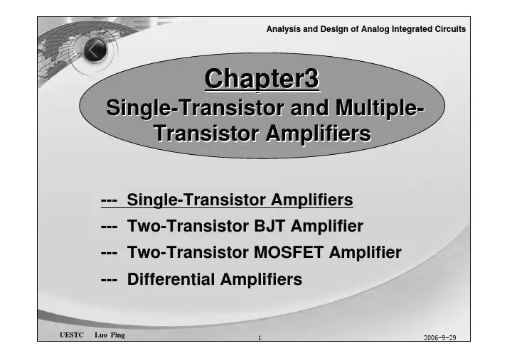
Chapter3Single-Transistor and Multiple-Transistor Amplifiers---Single-Transistor Amplifiers---Two-Transistor BJT Amplifier---Two-Transistor MOSFET Amplifier---Differential AmplifiersQuestions--Why we need to learn amplifiers?--What is amplifiers?--What will we learn about amplifiers? --How to learn?mv ,µvAmplifier is a key circuitWe need amplifiers*Microphone*Communications-Wireless -Optical-fiber *Disk Drive Electronics *Processing of Natural *Signals-SensorsWhat is amplifiers?What will we learn about amplifiers?*Basic configurations of amp.*The main characteristics of amp. we care*How to analyze & design amp.--Signal:Large Signal, Small Signal(*)--Model:LSM, SSM(*), Two-Port Model--Parameter:Device parameter:β, g m, rπ, r o(r ds), Cµ, CπCircuit parameter: R in, R out, A V,Frequency characteristics:ωL,ωH,ωT; f L, f H, f TGain, speed, power dissipation, noise,…22212122121111i g v g v i g v g i +=+=22212122121111v h i h i v h i h v +=+=22212122121111v y v y i v y v y i +=+=22212122121111i z i z v i z i z v +=+=g-parameter------voltage amplifier;h -parameter------current amplifier (hybrid);y-parameter------feedback amplifier (admittance); z-parameter------feedback amplifier (impedance).How to learn?--Distinguishdifferentcharacteristics ofdifferent amp.--Different design thought betweenIC circuits designand discreteelements circuitsdesign--Notice operation conditionsActive LoadtWLR ρ=19500001.00001.09500=Ω⋅==cm cm Rt WL ρ52.31=⎟⎠⎞⎜⎝⎛L L W 03.91 =⎟⎠⎞⎜⎝⎛L L WAnalog design octagonNoisePowerDissipationInput/Output ImpedanceSpeedVoltage SwingSupply VoltageGainLinearityIntuitionExperienceBasic Single-Transistor Amplifiers Outline---Characterizing an amplifier---BJT Single transistor amplifiers---MOS Single transistor amplifiers---Amplifiers with emitter/source degenerationCharacterization of AmplifiersAmplifiers will be characterized by the following properties•Large-signal voltage transfer characteristics (.DC)•Large-signal voltage swing limitations (.DC and .TRAN)•Small-signal, frequency independent performance (.TF)•Gain (.TF)•Input resistance (.TF)•Output resistance (.TF)•Small-signal, frequency response (.AC)•Noise (.NOISE)•Power dissipation (.OP)•Slew rate (.TRAN)Types of Single Transistor AmplifiersTypes of Single Transistor Amplifiers⎥⎦⎤⎢⎣⎡⎟⎟⎠⎞⎜⎜⎝⎛==T BE FO S F CB V v I i i exp ββ⎥⎦⎤⎢⎣⎡⎟⎟⎠⎞⎜⎜⎝⎛=T BE F S E V v I i exp α⎥⎦⎤⎢⎣⎡⎟⎟⎠⎞⎜⎜⎝⎛=TBES C Vv I i exp Signal Flow in TransistorsBo C I I β=CC CC CE R I V V ⋅−=Large-Signal:),(CE C V I Q Common Emitter AmplifierTCm V I g =CAo I V r =moin g r R βπ==Co out R r R //=)//(C o m inoutV R r g v v A −==Co oo C C o m in C out in out I R r r R r R r g r v R v i i A +====.).//(//βππmOg r βπ=Small-Signal:Large-Signal:2')(2tn GS nDSV V LW K I −=DDS DD DS R I V V ⋅−=),(DS DS V I Q Common Source Amplifier∞=in R Dds out R r R //=)//(D ds m inoutV R r g v v A −==∞≈=inoutI i i A Do Dnm I r r LWI k g λπ12'=∞==Small-Signal:Common Base Amplifier Large-Signal:Neglecting r o ,mo m m in g r g g g r R 111)1//(≈+=+==βπππCout R R ≈Cm inoutV R g v v A ≈=OO in outI i i A ββ+−≈=1Small-Signal:Common Gate Amplifier Large-Signal:Small-Signal:Neglecting rds,min g R 1≈Dout R R ≈Dm inoutV R g v v A ≈=1−==inoutI i i ALarge-Signal:BEIN OUT V V V −=Common Collector Amplifier (Emitter Follower)Large-Signal:GSIN OUT V V V −=Common Drain Amplifier (Source Follower)Neglecting r o ,Eo in R r R )1(βπ++=mo outg r R 11=+=βπEm Em in out V R g R g v v A +==1)1(o inoutI i i A β+−==Small-Signal:Neglecting rds,∞=in R Sm Sm S outRg R g R R +==1)1//(11<+==Sm Sm in out V R g R g v v A ∞==inoutI i i A Small-Signal:Solution:mSmVmA V I g T C m 5.38261===Ω===k mSg r m o62.25.38100βπΩ===k mAV I V r C A o 1001100Example 1-CE BJT circuitFind the small-signal R in , R out , v out /v in , and i out /i in for the circuit shown. Assume that βo =100, V A = 100V.Small-signal model is:Ω=+=k r R R S in 62.12πΩ==k R R r R L C o out 96.1////VV R r R g v v v v v v A inout m in out in out V /66.15)62.12/62.2)(96.15.38())(())((−=⋅−=−===πππAA k mS r R r R R r g i v v i i i A Co L C o m in out in out I /78.19)62.2)(549.7(].//)//([))((=Ω=+===πππExample 1-CE BJT circuitSolution:SLWI K g D Nm µ6632001011022'=×××==Ω=×==k I r D N ds 12520004.01016λFind the small-signal R in , R out and v out/v in of the common gate amplifier including r ds . Assume that K N ’=0.11mA/V^2, V t =0.7V, I D = 0.2mA and R D =20k.Example 2-CG MOSFET CircuitSolution:First find the small-signal model parameters.Ω=+Ω=++==k k r g R r i v R ds m D ds in in in 728.19.8211451Din ds in m in in R i r v g i v +−=)(V V G g g g v v v G v v g v g D ds ds m in out outD out in ds in m /57.115088663)(=++=++=→=−+Ω==k R r R D ds out 24.17//Solution:Example 2-CG MOSFET Circuit Using the small-signal model we get,A nodal equation at the output is given by:BJT Single Transistor Amplifiersπr om r g r βππ+=1/1//Eo R r )1(βπ++Co R r //Co R r //OS R r βπ+1//)//(L o m R r g −)//(L o m R r g Oβα−)1(O β+−Current Gain1Voltage Gain(Low)(High)(High)Output Resistance(High)(Low)(Medium)Input ResistanceCommon CollectorCommon BaseCommon EmitterSmall-Signal Performance SUMMARYMOSFET Single Transistor Amplifiers∞mg /1≈∞Dds R r //Dds R r //0 if /1or1=+S m S m SR g R g R )//(D ds m R r g −)//(D ds m R r g srm sr m R g R g +1∞∞-1Current GainVoltage Gain (Low)(High)(High)Output Resistance(Low)Input ResistanceCommon DrainCommon GateCommon Source Small-Signal Performancemoin g r R βπ==Eo B in R r R R )1(βπ+++=oo B E E B Eo out r r R R r R R R r R )1()//(]1[0ββππ+≈+++++=Co out R r R //=Common Emitter with Emitter DegenerationoV Cinin in C out in out I A R R R v R v i i A β≈−=−==//ECE B C m in C m in out V R R R r R R r g v R v g v v A −≤+++−=−≈=)1(0βπππ)//(C o m V R r g A −=Co oo I R r r A +=.βCommon Emitter with Emitter DegenerationMaximum gain!∞=in R Sm ds S S m ds out R g r R R g r R ≈++=]1[SDS m D m in out V R R R g R g v v A −≤+−==1Maximum gain!Common Source with Source DegenerationExample 3Ω===Ω======≥=⋅==Ω=Ω===K mAVI V r and mS mS mA mA V I Now Note mAI I uAK VFor C A o T C B F C 168.798.650 6.27926875g r ,2692698.6g ,r ,r ,g ,parameters signal small the of value the find .)2 )region active forward in is BJT so v v ( 98.6 931003.9100K (on)V -10V I I of value dc for the solve 1.)First, :Solution 50V V and 75 if /v v gain, voltage the and R ,resistance output ,R ,resistance input signal small the find shown,amplifier BJT pnp the m 0m 0m (sat)CE CE B B C AP F in out out in βββππVV R R r R g K r in B out m B /33.27)1279279()3.125()//)((v v as,found is gain voltage the Finally, 6.)467/1)K (7.168//1///R //R r R gives, resistance output for the Solving .)51297100//2781000//r R R gives,resistance input for the Solving 4.)as,writen be can amplifier the of mode signal -small The .)3inout L C o out s in −=×−=⋅−=Ω=Ω==Ω=+=+=ππOP Amp in Analog Circuit。
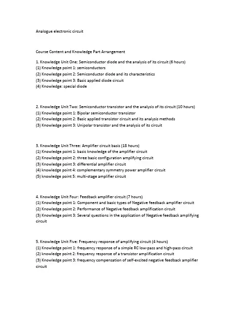
Analogue electronic circuitCourse Content and Knowledge Part Arrangement1. Knowledge Unit One: Semiconductor diode and the analysis of its circuit (6 hours)(1) Knowledge point 1: semiconductors(2) Knowledge point 2: Semiconductor diode and its characteristics(3) Knowledge point 3: Basic applied diode circuit(4) Knowledge: special diode2.Knowledge Unit Two: Semiconductor transistor and the analysis of its circuit (10 hours)(1) Knowledge point 1: Bipolar semiconductor transistor(2) Knowledge point 2: Basic applied transistor circuit and its analysis methods(3) Knowledge point 3: Unipolar transistor and the analysis of its circuit3.Knowledge Unit Three: Amplifier circuit basis (18 hours)(1) Knowledge point 1: basic knowledge of the amplifier circuit(2) Knowledge point 2: three basic configuration amplifying circuit(3) Knowledge point 3: differential amplifier circuit(4) knowledge point 4: complementary symmetry power amplifier circuit(5) knowledge point 5: multi-stage amplifier circuit4.Knowledge Unit Four: Feedback amplifier circuit (7 hours)(1) Knowledge point 1: Component and basic types of Negative feedback amplifier circuit(2) Knowledge point 2: Performance of Negative feedback amplification circuit(3) Knowledge point 3: Several questions in the application of Negative feedback amplifying circuit5. Knowledge Unit Five: Frequency response of amplifying circuit (4 hours)(1) Knowledge point 1: frequency response of a simple RC low-pass and high-pass circuit(2) knowledge point 2: frequency response of a transistor amplification circuit(3) Knowledge point 3: frequency compensation of self-excited negative feedback amplifier circuit6.Knowledge Unit Six: Analog Integrated Amplifier Application Circuit (9 hours)(1) Knowledge point 1: basic arithmetic circuit(2) Knowledge point 2: active filter(3) Knowledge point 3: voltage comparator(4) Knowledge point 4: non-sine wave generator7.Knowledge Unit Seven: Integrated analog multiplier and its basic application (2 hours)(1) Knowledge point 1: integrated analog multiplier(2) Knowledge point 2: variable transconductance analog multiplier(3) Knowledge point 3: analog multiplier applications8.Knowledge Unit 8: DC circuit (6 hours)(1) Knowledge point 1: single-phase rectifier and filter circuit(2) Knowledge point 2: Linear integrated voltage regulator(3) Knowledge point 3: switch integrated stabilized voltage supplyTotal class hours 64, include lecture class 52 hours, exercise and discuss class 12 hours, experiments to be arranged separately.Class Hours Associate Sheet。
模拟cmos集成电路设计英文版IntroductionA complementary metal-oxide-semiconductor (CMOS) integrated circuit (IC) is a type of electronic circuit that uses CMOS technology to integrate digital or analog circuits on a single chip. In this article, we will discuss the design process for a CMOS IC.Design flowThe design flow for a CMOS IC involves several stages, which are as follows:1. Requirements gathering: This stage involves gathering information about the requirements of the IC, such as its functionality, performance, and power requirements.2. Design specification: Based on the requirements gathered in the previous stage, a design specification is created that outlines the functional blocks of the IC, their interfaces, and their performance specifications.3. Circuit design: This stage involves designing the individual circuits that make up the IC, such as logic gates, amplifiers, and oscillators.4. Layout design: Once the circuits have been designed, the layout design stage involves placing the circuits on the chip and wiring them together.5. Simulation and verification: Simulation is used to verify the performanceof the circuits and the entire IC before it is fabricated.6. Tape-out: This is the process of preparing the design files for fabrication.Fabrication processThe fabrication process of a CMOS IC involves several steps, which are as follows:1. Substrate preparation: The starting material for the IC is a silicon wafer, which is coated with a layer of oxide.2. Gate oxidation: A thin layer of oxide is grown on the wafer surface where the gates of the transistors will be located.3. Poly-Si deposition: A layer of polycrystalline silicon (poly-Si) is deposited on the gate oxide layer.4. Photolithography: A series of masks are used to define the pattern of the transistors, interconnects, and other features on the chip.5. Etching: Chemical etching is used to remove the unwanted material from the wafer surface.6. Implantation: Ions are implanted into the wafer to create the source, drain, and gate regions of the transistors.7. Metal deposition: A layer of metal is deposited on top of the transistorsand interconnects for electrical contacts.8. Planarization: Chemical-mechanical polishing is used to planarize the surface of the chip.9. Packaging: The IC is packaged in a protective casing and tested for functionality and performance.ConclusionThe design and fabrication of a CMOS IC involves a complex process that requires expertise in multiple areas, such as digital and analog circuit design, layout design, and fabrication technology. However, the resulting IC can be a powerful tool for a wide range of applications, from consumer electronics to industrial control systems.。