SN54ALVTH16501资料
- 格式:pdf
- 大小:241.50 KB
- 文档页数:11
SN54ALVTH16501, SN74ALVTH16501
2.5-V/3.3-V 18-BIT UNIVERSAL BUS TRANSCEIVERS
WITH 3-STATE OUTPUTS
SCES071A – JUNE 1996 – REVISED JULY 1996
1
POST OFFICE BOX 655303 •
DALLAS, TEXAS 75265D
Members of the Texas Instruments
Widebus™ Family
D
High-Impedance State During Power Up
and Power Down
D
5-V I/O Compatible
D
High-Drive Outputs (–32 mA/64 mA)
D
Typical V
OLP (Output Ground Bounce)
< 0.8 V at V
CC = 3.3 V, T
A = 25°C
D
Auto 3-State Eliminates Bus Current
Loading When Voltage at the Output
Exceeds V
CC
D
Bus-Hold Data Inputs Eliminate the Need
for External Pullup/Pulldown Resistors
D
Power Off Disables Inputs/Outputs,
Permitting Live Insertion
D
Package Options Include Plastic 300-mil
Shrink Small-Outline (DL), Thin Shrink
Small-Outline (DGG), Thin Very
Small-Outline (DGV) Packages, and 380-mil
Fine-Pitch Ceramic Flat (WD) Package
description
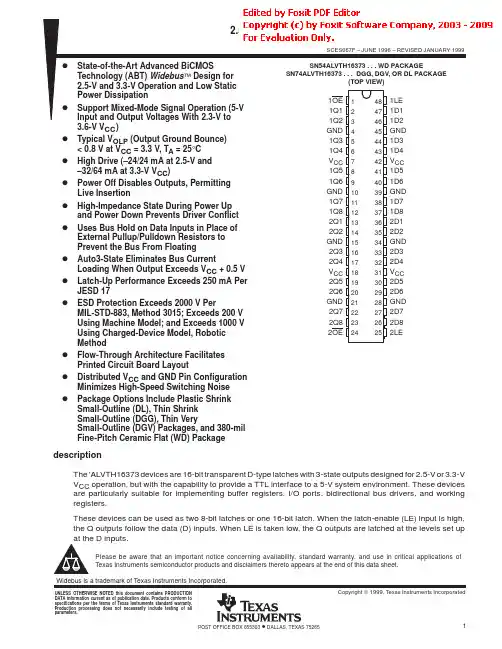
The ’ALVTH16501 are 18-bit universal bus
transceivers designed for 2.5-V or 3.3-V V
CC
operation, but with the capability to provide a TTL
interface to a 5-V system environment.
Data flow in each direction is controlled by
output-enable (OEAB and OEBA), latch-enable
(LEAB and LEBA), and clock (CLKAB and
CLKBA) inputs. For A-to-B data flow, the devices
operate in the transparent mode when LEAB is
high. When LEAB is low, the A data is latched if CLKAB is held at a high or low logic level. If LEAB is low, the
A-bus data is stored in the latch/flip-flop on the low-to-high transition of CLKAB. When OEAB is high, the B-port
outputs are active. When OEAB is low, the B-port outputs are in the high-impedance state.
Data flow for B to A is similar to that of A to B but uses OEBA, LEBA, and CLKBA. The output enables are
complementary (OEAB is active high and OEBA is active low).
Active bus-hold circuitry is provided to hold unused or floating data inputs at a valid logic level.
When V
CC is between 0 and 1.2 V, the device is in the high-impedance state during power up or power down.
However, to ensure the high-impedance state above 1.2 V, OE should be tied to V
CC through a pullup resistor
and OE should be tied to GND through a pulldown resistor; the minimum value of the resistor is determined by
the current-sinking/current-sourcing capability of the driver.
Copyright © 1996, Texas Instruments IncorporatedPlease be aware that an important notice concerning availability, standard warranty, and use in critical applications of
TexasInstruments semiconductor products and disclaimers thereto appears at the end of this data sheet.
Widebus is a trademark of Texas Instruments Incorporated.SN54ALVTH16501...WD PACKAGE
SN74ALVTH16501...DGG, DGV, OR DL PACKAGE
(TOP VIEW)
1
2
3
4
5
6
7
8
9
10
11
12
13
14
15
16
17
18
19
20
21
22
23
24
25
26
27
2856
55
54
53
52
51
50
49
48
47
46
45
44
43
42
41
40
39
38
37
36
35
34
33
32
31
30
29OEAB
LEAB
A1
GND
A2
A3
V
CC
A4
A5
A6
GND
A7
A8
A9
A10
A11
A12
GND
A13
A14
A15
V
CC
A16
A17
GND
A18
OEBA
LEBAGND
CLKAB
B1
GND
B2
B3
V
CC
B4
B5
B6
GND
B7
B8
B9
B10
B11
B12
GND
B13
B14
B15
V
CC
B16
B17
GND
B18
CLKBA
GND
PRODUCT PREVIEW
PRODUCT PREVIEW information concerns products in the formative or
design phase of development. Characteristic data and other
specifications are design goals. Texas Instruments reserves the right to
change or discontinue these products without notice.SN54ALVTH16501, SN74ALVTH16501
2.5-V/3.3-V 18-BIT UNIVERSAL BUS TRANSCEIVERS
WITH 3-STATE OUTPUTS
SCES071A – JUNE 1996 – REVISED JULY 1996
2
POST OFFICE BOX 655303 •
DALLAS, TEXAS 75265description (continued)
The SN74ALVTH16501 is available in TI’s thin very small-outline package (DGV), which provides the same I/O
pin count and functionality of standard Widebus packages in less than half the printed circuit board area.
The SN54ALVTH16501 is characterized for operation over the full military temperature range of –55°C to
125°C. The SN74ALVTH16501 is characterized for operation from –40°C to 85°C.
FUNCTION TABLE†
INPUTS
OUTPUT
OEABLEABCLKABAB
LXXXZ
HHXLL
HHXHH
HL↑LL
HL↑HH
HLHXB
0‡
HLLXB
0§
†
A-to-B data flow is shown; B-to-A flow is similar but
uses OEBA, LEBA, and CLKBA.
‡
Output level before the indicated steady-state input
conditions were established, provided that CLKAB
was high before LEAB went low
§
Output level before the indicated steady-state input
conditions were establishedPRODUCT PREVIEW